Your browser does not fully support modern features. Please upgrade for a smoother experience.
Submitted Successfully!
 +1 credit
Thank you for your contribution! You can also upload a video entry or images related to this topic.
For video creation, please contact our Academic Video Service.
| Version | Summary | Created by | Modification | Content Size | Created at | Operation |
|---|---|---|---|---|---|---|
| 1 | Khadijeh Miarabbas Miarabbas Kiani | + 1042 word(s) | 1042 | 2022-01-29 07:56:20 | | | |
| 2 | Conner Chen | -15 word(s) | 1027 | 2022-02-17 05:08:20 | | | | |
| 3 | Conner Chen | -17 word(s) | 1025 | 2022-02-17 05:15:19 | | | | |
| 4 | Conner Chen | -17 word(s) | 1025 | 2022-02-17 05:17:26 | | |
Video Upload Options
We provide professional Academic Video Service to translate complex research into visually appealing presentations. Would you like to try it?
Cite
If you have any further questions, please contact Encyclopedia Editorial Office.
Miarabbas Kiani, K. Microring Resonators. Encyclopedia. Available online: https://encyclopedia.pub/entry/19483 (accessed on 24 June 2026).
Miarabbas Kiani K. Microring Resonators. Encyclopedia. Available at: https://encyclopedia.pub/entry/19483. Accessed June 24, 2026.
Miarabbas Kiani, Khadijeh. "Microring Resonators" Encyclopedia, https://encyclopedia.pub/entry/19483 (accessed June 24, 2026).
Miarabbas Kiani, K. (2022, February 16). Microring Resonators. In Encyclopedia. https://encyclopedia.pub/entry/19483
Miarabbas Kiani, Khadijeh. "Microring Resonators." Encyclopedia. Web. 16 February, 2022.
Copy Citation
Microring resonators are fundamental components of any high-refractive-index-contrast photonic platform. They are a highly sought-after cavity component because of their ability to achieve on-chip field enhancement as well as spectral filtering and fast modulation of optical signals.
microring resonator
silicon-on-insulator (SOI)
silicon photonics
optical microrings
tellurium oxide
1. Microring Resonator Fabrication and Design
The microring resonator structure is displayed in Figure 1. It consists of an integrated silicon microring and bus waveguide coated with a thin film of tellurium oxide (TeO2). The silicon structure was fabricated in a silicon photonics foundry on a wafer-scale SOI platform with a 220 nm silicon layer thickness and consists of a 30 µm-radius silicon microring constructed using a 0.5 µm-wide waveguide. The bus waveguide is 0.4 µm wide, and the point coupling gap is 1.0 µm. The structure was cladded with SiO2, and subsequently, a window on top of the microring resonator was etched to the silicon layer for use in the post-processing TeO2 deposition or unclad device experiments. A set of devices with identical dimensions but without the SiO2 cladding etched was also fabricated for comparison. Deep etching was used for end-facet preparation and wafer dicing. For the TeO2-clad devices, the structure was coated with a 270 nm-thick TeO2 film deposited using a room-temperature reactive RF co-sputtering post-processing step with 145 W of tellurium target sputtering power, 2.8 mTorr chamber pressure, and 12 and 7.6 sccm of argon and oxygen flow, respectively. The substrate temperature was set at 20 °C. A top-view scanning electron microscope (SEM) image and the cross-section diagram of the TeO2-coated Si microring resonator are displayed in Figure 1a,b, respectively. Figure 1c,d show the image of the experimental setup and a microscopic image of the microring resonator with an open window structure.
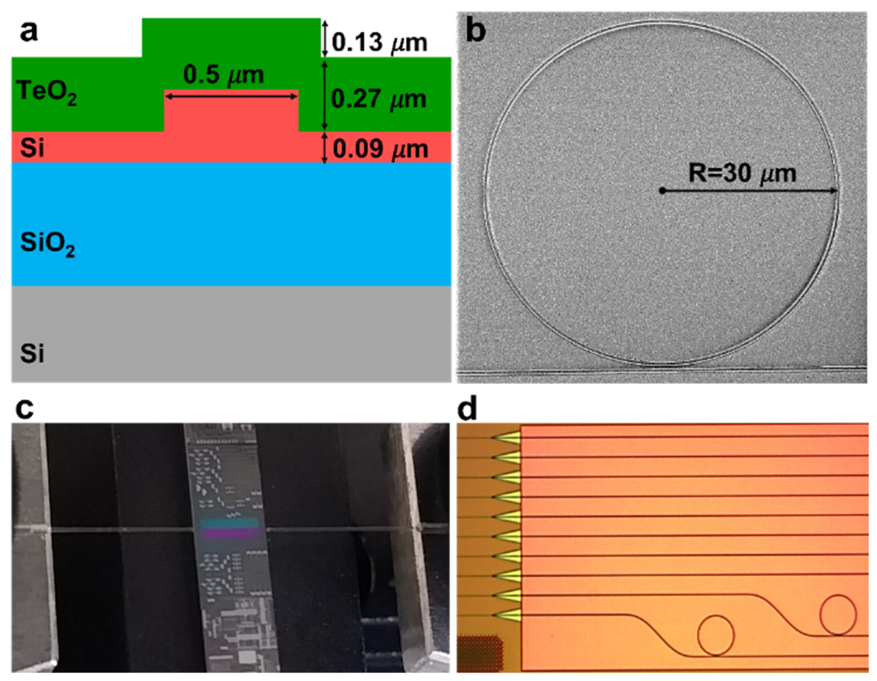
Figure 1. (a) Cross-section profile of the TeO2-coated Si microring showing the microring structure. (b) Top-view SEM image of a TeO2-coated Si microring resonator. (c) Photograph of the coupling setup during measurement showing the SOI chip with window opening for TeO2 post-processing deposition. (d) Microscopic image of the open window microring resonator structure.
The electric field profiles of the transverse-electric (TE)-polarized fundamental modes calculated using a finite element method (FEM) modesolver for the (cladding–core) TeO2–Si, SiO2–Si, and air–Si waveguides at a 1550 nm wavelength are displayed in Figure 2a–c, respectively. Summarizing the calculated optical properties of the TeO2–Si, SiO2–Si, and air–Si microring resonator structures in Figure 2d. The microring resonators and the bus waveguides were designed to achieve single-mode waveguide conditions at 1.55 to 2 μm wavelengths. The ring waveguide structure supports the TE-polarized and TM-polarized modes, and it has a low bending radiation loss at 1550 nm for TE only. The effective index of the TeO2-coated resonator is 2.8, which is almost 7.7 and 12% higher than that of the air- and SiO2-clad devices. For the TeO2-coated Si microring resonator, 21.7% of the optical power is confined in the TeO2 coating layer, while 65.0% is confined in the silicon layer. The rest of the optical power is confined in the lower SiO2 cladding. Slightly lower cladding confinement of 15.8 and 17.2%, respectively, is observed in the air- and SiO2-clad cases. The effective area is slightly larger in the TeO2-coated Si microring resonator than SiO2-coated and uncoated silicon microring resonators, although the mode is pulled upward more into the cladding, both of which can influence the ring–bus waveguide coupling.
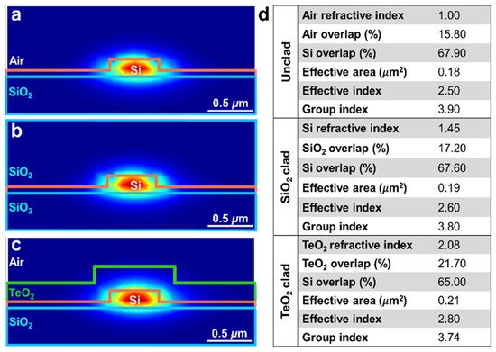
Figure 2. Calculated electric field profile of the fundamental transverse-electric (TE)-polarized mode for (a) unclad, (b) SiO2-clad, and (c) TeO2-clad silicon microring resonators. (d) Calculated fractional optical intensity overlap factors and effective mode areas for the fundamental TE microring mode at 1550 nm wavelength.
The TeO2-coated resonator has a higher mode area of approximately 0.20 μm2 at 1.55 μm. The effective index increases for the TeO2 film cladding as the resonant mode becomes more confined in the TeO2 layer. The expansion of the optical mode at longer wavelengths decreases the effective index. The results show that approximately 60% of the mode power is confined in the Si region and 26% in the TeO2-cladded layer for the TeO2 cladding at a wavelength of 1.55 μm.
2. Microring Resonator Characterization
The surface scattering loss is the waveguide scattering loss per unit length and was calculated using the widely used Payne–Lacey model [1]. This model has been applied previously to 3D-SOI bent waveguides [2][3][4] such that
where σ, k0, W, and n1 are the roughness, free-space wave vector, waveguide width, and core index, respectively. The function f is determined by the correlation length (Lc), while g is determined by the geometry of the waveguide and accounts for ridge-type waveguide structures such as the SOI ridge rings investigated here. Both σ and Lc are typically measured via atomic force microscopy or scanning electron microscopy of a waveguide. The values of σ and Lc are assumed to be 1.0 nm and 50 nm, respectively, based on previous measurements on SOI waveguides [2][3][4][5]. The roughness of the TeO2 coating is assumed to be negligible based on previous AFM roughness measurements showing <1 nm root mean square (RMS) surface roughness on low-loss sputtered thin films [5]. Details of the expressions g and f can be found in the Payne–Lacey model [1]. The Payne–Lacey model was modified for bent waveguides and rings by adding a correction factor η [2] which allows to accurately predict the loss of bent waveguides or resonators given the value of the sidewall roughness. The correction factor η is defined as the ratio of the mode overlap between bent and straight waveguides using an FEM simulation. In the Payne–Lacey bending model, η is considered 1 in the straight waveguide. Sidewall scattering losses are plotted as a function of wavelength. The experimental loss obtained from the quality factor measurements of the MRRs follows the same trend as the Payne–Lacey model, which indicates that the losses in the different MRRs are largely influenced by the core cladding refractive index contrast and sidewall roughness [6]. These results show that the application of a high-refractive-index TeO2 top cladding can be considered promising for low-loss passive components as well as active devices such as monolithic amplifiers and lasers with improved performance on the SOI platform [7].
References
- Payne, F.P.; Lacey, J.P.R. A theoretical analysis of scattering loss from planar optical waveguides. Opt. Quantum Electron. 1994, 26, 977–986.
- Hagan, D.E.; Knights, A.P. Mechanisms for optical loss in SOI waveguides for mid-infrared wavelengths around 2 μm. J. Opt. 2017, 19, 025801.
- Yap, K.P.; Delâge, A.; Lapointe, J.; Lamontagne, B.; Schmid, J.H.; Waldron, P.; Syrett, B.A.; Janz, S. Correlation of Scattering Loss, Sidewall Roughness and Waveguide Width in SiO2/Si Silicon-on-Insulator (SOI) Ridge Waveguides. J. Lightwave Technol. 2009, 27, 3999–4008.
- Shang, H.; Sun, D.; Yu, P.; Wang, B.; Yu, T.; Li, T.; Jiang, H. Investigation for Sidewall Roughness Caused Optical Scattering Loss of Silicon-on-Insulator Waveguides with Confocal Laser Scanning Microscopy. Coatings 2020, 10, 236.
- Miller, J.W.; Chesaux, M.; Deligiannis, D.; Mascher, P.; Bradley, J.D.B. Low-loss GeO2 thin films deposited by ion-assisted alternating current reactive sputtering for waveguide applications. Thin Solid Films 2020, 709, 13816.
- Zhang, L.; Jie, L.; Zhang, M.; Wang, Y.; Xie, Y.; Shi, Y.; Dai, D. Ultrahigh-Q silicon racetrack resonators. Photon. Res. 2020, 8, 684–689.
- Miarabbas Kiani, K.; Frankis, H.C.; Naraine, C.M.; Bonneville, D.B.; Knights, A.P.; Bradley, J.D.B. Lasing in a hybrid rare-earth silicon microdisk. Laser Photon. Rev. 2022, 16, 210034.
More
Information
Subjects:
Telecommunications
Contributor
MDPI registered users' name will be linked to their SciProfiles pages. To register with us, please refer to https://encyclopedia.pub/register
:
View Times:
1.7K
Revisions:
4 times
(View History)
Update Date:
17 Feb 2022
Table of Contents


Notice
You are not a member of the advisory board for this topic. If you want to update advisory board member profile, please contact office@encyclopedia.pub.
OK
Confirm
Only members of the Encyclopedia advisory board for this topic are allowed to note entries. Would you like to become an advisory board member of the Encyclopedia?
Yes
No
${ textCharacter }/${ maxCharacter }
Submit
Cancel
Back
Comments
${ item }
|
${ item.createdUser.fullName }
${ item.createdAt }
${ item.vote }
${ item.reply }
Delete
${ reply.createdUser.fullName }
${ reply.createdAt }
${ reply.vote }
Delete
There is no reply to this comment~
${ item.replyTextCharacter }/${ item.replyMaxCharacter }
Submit
Cancel
More
No more~
There is no comment~
${ textCharacter }/${ maxCharacter }
Submit
Cancel
${ selectedItem.replyTextCharacter }/${ selectedItem.replyMaxCharacter }
Submit
Cancel
Confirm
Are you sure to Delete?
Yes
No