Submitted Successfully!
To reward your contribution, here is a gift for you: A free trial for our video production service.
Thank you for your contribution! You can also upload a video entry or images related to this topic.
Version Summary Created by Modification Content Size Created at Operation
1 + 8996 word(s) 8996 2022-01-24 07:51:19 |
2 format correct + 1 word(s) 8997 2022-01-27 02:54:19 |

Video Upload Options

Do you have a full video?

Confirm

Are you sure to Delete?
Cite
If you have any further questions, please contact Encyclopedia Editorial Office.
Faraji, S. Solution-Processed Organic Phototransistors and Their Recent Developments. Encyclopedia. Available online: https://encyclopedia.pub/entry/18860 (accessed on 18 May 2024).
Faraji S. Solution-Processed Organic Phototransistors and Their Recent Developments. Encyclopedia. Available at: https://encyclopedia.pub/entry/18860. Accessed May 18, 2024.
Faraji, Sheida. "Solution-Processed Organic Phototransistors and Their Recent Developments" Encyclopedia, https://encyclopedia.pub/entry/18860 (accessed May 18, 2024).
Faraji, S. (2022, January 26). Solution-Processed Organic Phototransistors and Their Recent Developments. In Encyclopedia. https://encyclopedia.pub/entry/18860
Faraji, Sheida. "Solution-Processed Organic Phototransistors and Their Recent Developments." Encyclopedia. Web. 26 January, 2022.
Solution-Processed Organic Phototransistors and Their Recent Developments
Edit

Today, more disciplines are intercepting each other, giving rise to “cross-disciplinary” research. Technological advancements in material science and device structure and production have paved the way towards development of new classes of multi-purpose sensory devices. Organic phototransistors (OPTs) are photo-activated sensors based on organic field-effect transistors that convert incident light signals into electrical signals. The organic semiconductor (OSC) layer and three-electrode structure of an OPT offer great advantages for light detection compared to conventional photodetectors and photodiodes, due to their signal amplification and noise reduction characteristics. Solution processing of the active layer enables mass production of OPT devices at significantly reduced cost. The chemical structure of OSCs can be modified accordingly to fulfil detection at various wavelengths for different purposes. Organic phototransistors have attracted substantial interest in a variety of fields, namely biomedical, medical diagnostics, healthcare, energy, security, and environmental monitoring. Lightweight and mechanically flexible and wearable OPTs are suitable alternatives not only at clinical levels but also for point-of-care and home-assisted usage.

solution-processed organic phototransistor organic photodetector organic semiconductor low-voltage OFETs optical memory OPTs for biomedical and information technology

1. Introduction

A phototransistor (PT) is a type of photodetector that converts an incident light signal into a detectable electrical signal. This three-electrode device amplifies the signal, reduces the noise and hence provides superior functionality compared to other photodetector devices, such as photodiodes [1][2][3][4]. Phototransistors have been used for decades in a variety of fields such as medical applications, optical communications, environmental and industrial studies, disaster weather prediction and fire warning (Figure 1). Taking the medical sector as an example, by benefiting from such novel optical devices in medicine and biomedical applications, more reliable and rapid diagnosis and treatment are achieved. Technological and scientific needs lead to inventing new means of optoelectronic devices, in particular, those based on field-effect transistor (FET) [2][5][6][7][8].
Figure 1. Examples of the application areas for PTs.
Conventional phototransistors are based on inorganic semiconductors which are IV, III–V and II–VI groups of periodic table [4][7][9][10][11]. The most well-known examples of PTs are based on Si from the IV group and GaAs, InGaAs from the III–V group. Phototransistors’ working wavelength range differs depending on the semiconductor type. Generally, Si is used for the visible (Vis) to near infrared (NIR) range, while InGaAs is used in the NIR region [11]. Each region in the spectrum has various application areas related to their wavelength and the semiconductor bandgap. UV sensitive photodetectors are designed to be utilized in communication, security and medical. In NIR and IR range, biomedical and artificial vision are probed [11][12][13][14]. However, Si-based PTs are insufficient to be used in NIR [2]. In addition, these traditional inorganic semiconductors are not promising materials for wearable, flexible phototransistors in home-assisted or clinical sensor applications due to their rigid structure, and their high-cost production conditions are not suitable for cost-effective, high throughput technologies [4][7][15][16]. Organic materials, polymers and small molecules being the most common types, have opened up new opportunities to overcome the aforementioned drawbacks [17][18][19].
Organic semiconductors (OSC) have shed light on mechanically flexible, soft, low-power, low-cost, non-invasive light optoelectronic devices for both industrial and clinical implementations. Thanks to their tunable molecular structure, OSCs’ bandgap can be tailored according to the targeted application. Not only the bandgap, but also the functionality of OSCs can be adjusted to enhance efficiency in the corresponding area of interest [3][8][11][19][20][21][22][23]. Owing to organic semiconductor materials’ easy processing, large-scale production, lightweight structure and solution-processable manufacturing, new classes of optical devices are realised.
The two main subcategories of photodetectors are photodiodes and phototransistors. Photodiode is commonly a two-terminal device with a vertical structure in which OSC layer is sandwiched between electrodes with an ohmic contact. Carriers are circulated until recombination occurs between symmetrical electrodes. As a result, photodiodes have >100% photoconductive gain and high responsivity. However, a phototransistor provides both high sensitivity and low noise levels and shows high detectivity compared to photodiodes. It can be explained by their transistor mechanism. The gate electrode plays a crucial role in modulating current and lowering noise. In addition, a phototransistor combines signal amplification and light detection in a single device. Hence, it can be integrated easily into devices and circuits. The active material can take the light directly without the shielding of electrodes as it is the case in photodiodes [2][3][12][18].
Organic phototransistors (OPTs) are optically controllable devices based on organic field-effect transistors (OFETs) [1][7][11][18][21][24][25][26][27]. OFETs play a crucial role in optoelectronic research due to their organic active layer, three-electrode device structure, signal amplifying properties, low noise medium and low voltage operation depending on the dielectric type. OSCs intrinsically provide efficient light absorption properties, tunable bandgap, lightweight, low-cost, and easy mass production by solution-processing. In general, OSCs are employed into OFETs as a thin film, hence OFET configuration is often referred to as organic thin-film transistor (OTFT) [3][17][28][29][30][31][32][33].
It should be noted that flexible organic phototransistors have been mainly investigated for detection in the UV-Vis range. For instance, C8BT-BT: PLA films were fabricated in both layered and blended forms and examined under 300–800 nm UV-Vis range with higher photocurrent (up to 105) is achieved from the latter, attributed to the charge trapping effect [25]. Recently, advances in OPTs with the main focus on UV, short-wave IR (SWIR) and near IR detection have risen substantially [19][33][34][35][36][37]. Numerous research on NIR sensors is increasingly leading to novel medical diagnosis and point-of-care developments, for instance, pulse oximetry and monitoring blood pressure [9][15]. Most basic human characteristics can be evaluated by the flow of blood in the subcutaneous tissue. “Therapeutic window” or “diagnostic window” is considered when studying the light absorption of the tissue. Biological tissues exhibit low absorbance. This explains why the long-wavelength range (600–1600 nm) of the NIR and SWIR (short wave infrared light) light detection is particularly used in OPTs for medical and biomedical studies [5][6][15][16][37]. DPP-DTT (poly (N-alkyl diketopyrrolopyrrole [3,2-b]thiophene) is one of the preferred OSC material for NIR optical sensors. From the literature, it is already known that DPP-DTT: PCBM solution- based bulk heterojunction (BHJ) is used as an active layer in OPT studies [9][15][36][38]. In addition, poly(5,7-bis(4-decanyl-2-thienyl)-thieno(3,4-b)diathiazole-thiophene-2,5) (PDD-TT) and 4,4-difluoro-4-bora-3a,4a-diaza-s-indacene (BODIPY-BF2) are also used as NIR-sensing materials [39][40].

2. Organic Semiconductors and Fundamental Principles of OFETs

Following their introduction in the 1980s, OFETs now have performance levels comparable to that of their polycrystalline (inorganic) counterparts and some organic semiconducting materials exhibit field-effect mobilities greater than 1 cm2 V s−1 [41][42].
To understand the OPT mechanism better, its beneficial to first study OSCs and OFETs. In Section 2.1, organic semiconductor structure, charge generation in OSC, different types of OSCs and their outstanding properties are explicated. An OFET has different device designs. Few considerations are taken into account when designing an OFET device. This three-electrode device’s working mechanism is focused on along with trap limited charge transport and contact resistance in Section 2.2. Finally, examples of conventional and new solution-processing techniques adopted for OFET and OPT fabrication are given in Section 2.3.

2.1. Organic Semiconductors

Organic semiconductors (OSCs) are carbon-based optoelectronic materials with unique solid-state physical properties stemming from the soft, van-der Waals bonding between their molecules [43]. They have exotic light detection capabilities, ranging from ultraviolet (UV) to Infrared (IR). They are used in OFETs, organic photovoltaics (OPVs) and photodetectors due to their fantastic features, such as soft molecular nature, mechanical flexibility, solution-processability, high-throughput, low-cost production, lightweight, absence of rare or toxic elements in their composition and eco-friendly nature [11][18][44][45][46]. They are popular choices of material that extensively explored in established and emerging optoelectronic applications. Moreover, the distinctive ability of OSCs to combine electronic and ionic conduction has made them appealing candidates in organic electrochemical transistors (OECTs) [47], chemical and biological sensors [48] and neuromorphic devices [49].
From a chemistry point of view, organic semiconductors have sp2 hybridization (Figure 2). σ bonds are much stronger than π bonds. The transition of electrons in π−π* orbitals require the lowest energy, and the conduction takes place more easily. Therefore, it is crucial to have sp2 hybridization to conduct electricity [50][51][52].
Figure 2. (a) chemical structure of ethylene, (b) σ and π bonds. Reprinted with permission from ref. [51]. Copyright 2017 Elsevier.
In organic semiconductors, charge carriers are called polarons [28]. Polarons are self-localized. Localization of charge carriers is associated with the hopping transport taking place in organic semiconductors [28][51]. Electrons hop from the highest occupied molecular orbital (HOMO) of the OSC to the lowest unoccupied molecular orbital (LUMO) of p-type semiconductors (and vice versa for n-type OSCs). For common OSCs, the bandgap can be 1–5 eV. In general, the smaller the bandgap is, the longer wavelength of light can be detected. This opens up new ways to benefit from organic semiconductors in optical devices for various applications.
Thanks to their tunable molecular structure, OSCs’ bandgap can be adjusted according to the desired application [2][11][53]. Not only the bandgap, but also the functionality of OSCs can be tuned to enhance the efficiency, sensitivity, and selectivity of the corresponding devices [3][11][19][20][21][22][23].
A comparison between organic and inorganic semiconductors along with their corresponding parameters is given in Table 1.
Table 1. A comparison of organic and inorganic semiconductor materials [45][50][51][54].
Parameter Organic SC Inorganic SC
Binding energy Weak (Van der Waals) Strong (Covalent, metallic, ionic bonding)
Mechanical resistance Weak (prone to gases and oxidation) Strong
Charge carriers Polarons, excitons (localized) e, h+, ions (delocalized)
Dielectric constant 3–4 11
Polarisation Strong Weak
Charge transport Hopping Band
Exciton Frenkel Wannier-Mott
Mobility ~10−6–1 cm2 V−1 s−1 ~1000 cm2 V−1 s−1
Conductivity Extrinsic Intrinsic
Organic molecules are composed of covalently bonded molecular units and their electron delocalization ability depends on the intermolecular packing. Some of the intermolecular modes are soft which means large vibrational amplitudes can occur at room temperature. Electronic and structural dynamics help to explain the charge transport and optoelectronic properties in OSCs. The structure–property relationship is one of the main aspects that guide scientists to understand electronic structure’s effect on charge transport and radically improve materials for application in optical devices [43]. Many examples of organic single crystals, thin films and nanowires used as the active layer in OPTs and OFETs are reported in the literature (Figure 3) [1][25][36][55][56][57].
Figure 3. Some examples of OSCs in a broad wavelength range of the spectrum. Reprinted with permission from ref. [3]. Copyright 2013 Wiley.
Thin films are key components of today’s technological advancements. Their features differ from those of the bulk materials due to the nanostructure form [58]. In recent years, there has been growing interest in organic dielectric and semiconducting thin films due to their compatibility with a wide range of materials, processing techniques and practical device structures [1][11][18][59]. For the semiconductor active layer, polymers, small molecules or/and polymer/small molecule blends are the most largely used candidates (Figure 3). Polymer organic phototransistors (PPTs) or small molecule organic phototransistors (SOPTs) take their names from the active layer material [3][18][28][45][46][51]. These materials can be easily deposited using solution processing techniques [3][11][18][46]. In particular, polymeric semiconductors exhibit superior solution-processing ability and compatibility with plastic substrates and can be used as pristine or in blends with small molecules in organic phototransistors. 

2.2. Fundamental Principles of OFETs

An organic field-effect transistor is a three-electrode device, also called an organic thin-film transistor (OTFT). Nowadays, numerous sensors are developed based on OFETs. From chemical sensors for volatile organic compounds (VOCs), NIR- sensitive phototransistors to biosensors based on microfluidic-OFET, field effect transistor is used in combination with other electronic structures because of OFETs’ comprehensive advantages [22][25][30][57][60][61][62][63][64][65][66]. First and foremost, mechanical flexibility, low processing temperature and chemical functionality are the critical properties of OFET devices. Moreover, one of their most important properties is the compatibility with a variety of substrate materials choices. Paper, textile or other biodegradable substrates can be utilized to reduce electronic waste [3][67][68][69][70].
An important difference to the other FET-based devices is that OFET works in the accumulation regime [28][62][71]. Basically, an OFET device is comprised of three components. One of them is the organic semiconductor serving as the active layer. The second component is the dielectric layer. It plays an important role in the OFET device due to its capacitor mission. In order to operate OFETs at low voltages, a dielectric layer with high dielectric constant (so-called high-k) is essential [72][73]. The last component is the electrodes, which are gate (G), source (S) and drain (D). There are different device configurations depending on the position of electrodes [60][74] that are given in Figure 4. The common configurations are the bottom gate/top contact (BG/TC), bottom gate/bottom contact (BG/BC), top gate/bottom contact (TG/BC) and top gate/top contact (TG/TC). OFETs with the same components do not show similar behaviour when they have different device configuration.
Figure 4. Different geometrical configurations of an OFET. (a) Bottom gate, top contact, (b) Bottom gate, bottom contact, (c) Top gate, bottom contact, (d) Top gate, top contact OFET.
The dielectric layer behaves like a capacitor between gate and source-drain electrodes. Charge carriers are stopped by the insulator layer, then they begin to accumulate [20][28][29][30][51][62][63]. That is why the OFET is working in the accumulation regime. The channel conductivity is modulated by means of the gate electrode. The role of the source and drain electrodes is to inject and withdraw charge carriers, respectively. When no voltage is applied to the gate electrode (VG = 0), very low current flows in the channel, so-called the “off-state”. After applying a gate voltage, the charge carriers are accumulated at the interface of the semiconductor/dielectric and a conductive active channel forms between source and drain. The sheet of mobile carriers at the interface leads to a higher current, which means the device is in the “on-state”. It is necessary to elucidate that the on-off state of an OFET device is related to the threshold voltage position [29][45][51][62][63].
In Figure 5, current-voltage (I–V) output and transfer characteristics of a typical OFET are illustrated. Figure 5c shows the linear dependence of the square root of the drain with the gate voltage [8].
Figure 5. A representative current-voltage characteristics, (a) output curve, (b) transfer curve in linear regime, and (c) in saturation regime. Reprinted with permission from ref. [8]. Copyright 2007 American Chemical Society.
An output curve demonstrates the drain current (IDS) versus source-drain voltage (VDS) at a constant gate voltage value. A transfer curve represents the drain current versus gate voltage at a constant VDS. With the help of Figure 5b, the onset voltage can be extracted from the semi-log plot (a quick step up of drain current above a defined low off-current). The subthreshold swing (SS = dVG/d(log(IDS))) depends on the gate dielectric capacitance and trap states. For an ideal OFET, the number of trap states is equal to zero, thus the theoretical minimum value of SS is calculated at room temperature as 59.5 mV decade−1 [33].
OFET has three modes that depend on the gate voltage (VG) and drain voltage (VDS): linear, saturation and cut-off (pinch-off) regions, respectively (Figure 6).
Figure 6. Illustrations of operating modes of OFETs, (a) linear regime, (b) start of saturation regime, (c) the channel pinch-off and saturation regime.
When VG is applied, while VDS is zero charges are induced at the insulator/semiconductor interface uniformly. When a small VDS is applied, charge carriers begin to move from source to drain through the active channel [28][30][31][45][62][63]. As seen in Figure 6, as VD (or VDS) value increases, the mode changes and goes to saturation regime. Drain current (or the channel current IDS) in linear and saturation regimes are shown by Equations (1) and (2), respectively:
I D = W L C i μ V G V th V D 2 V D ,   V D < V G V th
(1)
In   saturation :   I D = W 2 L C i μ sat V G V th 2 ,   V D > V G V th
(2)
In Equations (1) and (2), Ci is the areal capacitance of the dielectric; W is the channel width and L is the channel length. Ci is calculated as in Equation (3):
C i = ε r ε 0 d
(3)
In Equation (3), d is the thickness of the dielectric layer.
At an applied gate voltage higher than the Vth, the charges in the channel (Q) start to accumulate (Equation (4)) with respect to Ci and VG.
Q = C i V G V th
A larger capacitance value is required to lower the operating voltage. A high capacitance value allows accumulating more charge carriers at low applied voltage. There are some strategies to increase the Ci Equation (3). One of them is using high-k (εr) dielectric materials to induce more charges [31][33][75][76]. The other one is to decrease the dielectric thickness (~d < 20 nm). It should be noted that the dielectric thickness needs to be significantly thinner than the channel length (L > 10 ddielectric) in order to ensure that the gate voltage modulates the charges in the channel [8][29]. Conventional studies took silicon dioxide (SiO2) as both insulator layer and substrate on account of their smooth structure and availability, despite its low k-value (ε = 3.9). Other frequently chosen materials are metal oxides such as aluminium oxide (Al2O3ε = 8) and tantalum oxide (Ta2O5ε = 23). Meanwhile, low-k polymeric insulator materials such as polymethylmethacrylate (PMMA, ε ≈ 3.5), polyvinyl alcohol (PVA, ε ≈ 7.8) and poly(4-vinyl phenol) (PVP) have been utilized, as well. They are solution-processable and can be deposited on top or bottom depending on the device configuration. It is known from the literature that after solving in an orthogonal solvent, they can be applied on top of the OSC, and do not damage the OSC. Cellulose is also preferred as a natural high-k insulator material. Pure cellulose has a relatively higher k constant (k = 6–8) than other solution-processed polymers. Dry cellulose has air in its voids hence its k decreases to 1.5–4. To hinder this, fillers such as oil, resin, inorganic particles are made use of [67]. Cyanoethyl cellulose (CEC) and CEC-based nanocomposite (using nanoparticles of barium strontium titanate (BST, k ≈ 16)) dielectrics with PVP capping thin-films demonstrated have shown promises for low voltage, low power electronics [77]. Moreover, self-assembled monolayers (SAMs) came out as a modifying component that increases the capacitance by decreasing the thickness to a few nanometres. Hybrid dielectric materials have emerged to solve the problem of polymers’ low-k and inorganics’ high-temperature deposition process. Hybrid materials combine organic materials with inorganic ones. Thus, they benefit from organic materials’ easy deposition and flexibility and high capacitance of the inorganic ones. Researchers have shown growing interest in polymer-ceramic dielectrics. Polymeric-nanoparticle dielectric composites date back to 1988. Polystyrene (PS) and titanium oxide nanoparticles’ (TiO2 NPs) composite was one of the attempted high-k dielectric materials. BST and barium zirconate (BZ, k ≈ 11) NPs are used with high-k fluorinated polymers such as poly(vinylidene fluoride-co-hexafluoropropylene) (P(VDF-HFP)) to make use of their superior features. In these studies, NPs agglomeration can be a complication in obtaining homogenous nanocomposite suspensions. A careful combination of organic solvents and NP-to-polymer volume ratio can be sufficient enough to rule out any required surface modification [78]. Inorganic-organic bilayer is another way to make a hybrid dielectric, for instance PMMA/Ta2O5 [75]. Chen et al. reported development of [76] low-power OFETs with solution-processable nanocomposite of PVP and calcium titanate nanoparticles (CaTiO3 NPs, k ≈ 150) as the gate dielectric. For a p-type OFET, high work function metals, such as Au, Pt are chosen as the S/D electrodes. Devices operate by applying a negative voltage to the gate electrode (vice versa for n-type device) [28][29][44][62]. The larger the applied negative gate voltage is, the higher the induced holes appear in the conducting channel. By applying a negative drain voltage, holes begin to move to the drain electrode [29][45][62][65]. This is related to the HOMO-LUMO level of the semiconductor and the work function of the metal electrode [8][45][62]. Transition metal oxide (TMO)-based buffer layers, such as molybdenum trioxide (MoO3), vanadium oxide (V2O5), tungsten trioxide (WO3) are generally utilized to lower the hole injection barrier [79]. As shown in Figure 7, trap states exist in the HOMO-LUMO gap [80].
Figure 7. A presentation of the trap states between HOMO and LUMO. Reprinted with permission from ref. [80]. Copyright 2013 Royal Society of Chemistry.
Once deep levels are filled, charges can begin to transport through the channel by applying a VDS bias. Traps can increase not only the photosensitivity, but also the response time. For instance, for a p-type device, as more holes are trapped in the OSC, more electrons stay in the active channel due to charge neutrality. Therefore, the conductivity is increased. The insulator-semiconductor interface is defined as a high-trap density region [28][29][33][62][81]. This topic elucidated in more detail in Section 3.2.
The final characteristic we discuss here with respect to OFETs is contact resistance (RC). It is literally the total of source and drain contacts’ resistances. Due to charge injection from metals, charge carriers must pass a barrier. That is why it is called contact resistance. [29][45]. One of them is channel resistance (Rchannel). The Drain current–Gate voltage (transfer) curve is not a straight line because of contact resistance. Access resistance is another resistance that exists in the OFET structures. Travelling of charge carriers from the source into the channel and back up to the drain causes access resistance. It is also known as bulk resistance (Rbulk). In bottom gate- bottom contact (BGBC) structures, electrodes are in the same plane as the OFET channel, hence access resistance is not an issue in this case. Charges can be directly injected into the active channel layer at the insulator/semiconductor interface. In TC structure, the main source of the contact resistance is the access resistance. Charges must travel through a few nanometres to arrive at the channel. Access resistance can be negligible when using polycrystalline films due to their rough surface. [82]. When adopting top gate-bottom contact (TGBC) and bottom gate-top contact (BGTC) structures, charges can be injected from both the edge of the source electrode and the overlap region with the gate electrode [8]. Much research has been focusing on lowering the contact resistance by applying various methods, such as preferring TC over BG configurations due to poor semiconductor morphology in the latter. Apart from that, semiconductor’s surface quality can be improved by some chemical modifications. Thiol-terminated (R-SH) hydrocarbon molecules are frequently applied to form a SAM layer on the metal contacts to mask it from the semiconductor [83].

2.3. Solution Processing Techniques for Device Fabrication

The solution processing method is a promising deposition technique for fast, cost-effective, high-throughput production of electronic devices on flexible/conformal substrates. It is highly compatible with most organic semiconductors and polymeric dielectric materials. Ease of fabrication and real-time control of parameters due to low (room) temperature process makes such deposition techniques attractive for OFETs and OPT devices. Examples of widely adopted solution-processing techniques are spin coating, drop casting, dip coating, spray coating, blade coating (or roll-to-roll method) and gravure and inkjet printing. Nowadays, inkjet printing has been widely used because it offers superior advantages to frequently preferred spin-coating. Inkjet printing is a very fast method with low material consumption, printing ability of arbitrary patterns, and high resolution [84][85]. Inkjet printing does not require direct contact with the substrates which in return reduces the risk for defects induced by contact with mechanical parts. By adopting inkjet printing, direct deposition of controlled volume of functional materials is made possible via a material-efficient approach [86]. Fully inkjet-printed OFET prototypes are successfully attempted [87]. Nevertheless, inkjet printing is intrinsically slower than some other high-throughput printing methods, such as gravure. Parallelization (multi-nozzle) strategies are introduced to minimize such shortcomings [88]. The conventional channel length of inkjet-printed pattern is normally limited to about 10 μm. By using electric fields to produce the formation of a droplet (electrohydrodynamic jet printing), materials can be patterned down to a resolution of 1 μm [89]. Smaller channel lengths can be achieved through techniques integrating printing with a self-assembly-driven process, such as self-aligned printing, in which the surface energy of a pre-printed pattern is modified with SAMs or surfactants [90].
Not all but the majority of the small molecule and polymer OSCs can be deposited by solution processing. Polymeric OSCs have better solution-processability than small molecules. Blends of polymers and small molecules have been prepared to facilitate easier and scalable solution deposition [91]. Processing from solution enables tuning of molecular packing in OSC thin films [3][11][18][20][27][60][74]. Creating a highly ordered and uniform surface is critical for efficient charge transport and high-performance device. However, it is not always possible to obtain highly aligned organic crystalline arrays, due to the challenges over the controlling of crystallographic orientation. OSCs can be distracted due to their fragility by high temperature, UV light, or organic solvents. That means any subsequent photolithography techniques can impair the solution-processed thin films underneath [92][93]. Most recently, the solution shearing technique was adopted to successfully print water-soluble ink on a hydrophobic surface of an OFET device [92]. The solution shearing technique was chosen due to its simplicity and reformative feature on the molecular motifs [92][94]. In addition, this technique was combined with the screen-printing method; both of which are inviting techniques for high-quality industrial production. The fluid drying dynamics changed with the water-soluble surfactants which had been added to reduce the surface tension between OSC and resist. Highly aligned organic crystalline arrays were obtained in this study.

3. The Applications of Organic Phototransistors

Phototransistors have a wide variety of application areas, such as visible light detection, biomedical health monitoring, remote diagnostics, electronic eyes, industrial process inspection, food and water quality control, environmental surveillance, energy, optical memory, etc.
Recent advances on OPTs have been particularly focused on detection in the UV and NIR regions. UV sensors are gaining increasing attention for utilisation in the health and medical fields to prevent sunburn and skin cancer caused by sunlight [13][14][19][33][34][35][36][37]. Detection and quantification of the intensity of UV light plays a critical role in medical diagnostics. It has already been known that UV light can have a harmful effect on skin, and overdose exposure can lead to skin cancer. One must avoid to exposure to UV light without control and/or in the absence of safety measures. On the other hand, UV light is applied for phototherapy to cure skin diseases like atopic dermatitis. Under controlled conditions and uniform pulse output, UV light can be a very useful tool in the biomedical field. For instance, UV-B sensitive, low-voltage, solution-processed, thin-film phototransistor was developed for the safe and effective treatment of skin diseases [95]. To explore the effect of UV light on both causing and curing diseases, it is beneficial to carefully quantify the UV light. UV light is mainly divided into three groups: UV-A (400–320 nm), UV-B (315–280 nm) and UV-C (290–100 nm). Determination of the amount of UV-A and UV-B is done by some portable technologies. However, they do not offer high accuracy due to the continuous need for calibration. Dosimeters, sunscreens, UV-weakening clothes are some examples of UV exposure monitoring techniques [14]. Nevertheless, high accuracy, real-time devices are still required for the detection of UV light. Low-voltage, solution-processed organic phototransistors are promising candidates in this field to obtain fast and accurate results. One the other hand, numerous researche have been increasingly focused on development of near IR sensors for medical diagnostics, for instance, pulse oximetry and monitoring blood pressure [9][15]. Home-assisted (bio)medical sensors have gained more demand than ever before, due to increased hospitalisation and hospitals overcrowding during the COVID-19 pandemic [96][97][98][99]. Photoplethysmography (PPG) sensors can be integrated into home-assisted kits and offer tremendous advantage to monitor cardiovascular and atherosclerosis disease markers, such as heart rate (HR), blood pressure (BP), heart rate variability (HRV), arterial oxygen saturation (SpO2), arterial ageing. Most basic human characteristics can be evaluated by the flow of blood in the subcutaneous tissue. PPG sensors can detect these indicators by monitoring pulsatile changes in blood flow [100][101][102][103]. The device can be operated in two different modes: Reflective or transmitting mode. Several studies are reported excellent work on PPG sensors 
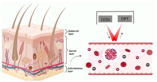
[104][105][106]. “Therapeutic window” or “diagnostic window” are taken into account when studying light absorption of the tissue. Biological tissues exhibit low absorbance. It explains why long penetration distance is critically considered in biomedical sensors, otherwise, the light is scattered by cells and proteins. The long-wavelength range (600–1600 nm) of the NIR and short-wave IR (SWIR) account for the absorption of the light throughout the tissue (Figure 16), which can penetrate deep subcutaneous part [5][6][15][16][37]. Red and NIR regions provide the largest contrast between the absorption of oxyhemoglobin (HbO2) and hemoglobin (Hb), thus enabling greater accuracy and selectivity in detection. Depending on the arterial pulse, the light absorption varies, and hence the optical density and path length changes [6][15].
Figure 16. Skin tissue and light absorption of erythrocytes. In this figure, the device mechanism is in reflective mode. This figure was created with BioRender.com (accessed on 26 May 2021).
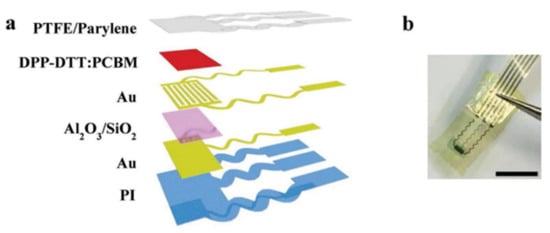
Xu et al. reported using solution-processed DPP-DTT: PCBM BHJ as an active layer in OPT devices as PPG sensors in the reflection mode [15]. In this study, a hybrid design was demonstrated (Figure 17). They utilised a 1.8 µm-thick polyimide (PI) as the substrate, due to its smooth surface, good chemical stability, biocompatibility and excellent thermal stability. The applied bilayer dielectric (Al2O3/SiO2) led to achieving low operating voltage (<3 V).
Figure 17. (a) Schematic of the device structure of the flexible OPT, (b) figure of a freestanding OPT. Reprinted with permission from ref. [15]. Copyright 2017 John Wiley & Sons.
To increase the mechanical stability of the sensor, PTFE/Parylene was used as the encapsulating layer. Comparing their device with commercial PPG and clinical ECG, they reported higher accuracy (0.3% error) and better performance than conventional ones, giving promises for low power and real-time monitoring sensors. For evaluating pulse pressure variation (PP mmHg) they compared their hybrid PPG (hPPG) and a commercial PPG (cPPG) with taking a reference PP. In different positions of volunteers, PP showed fluctuating results, and hPPG and reference PP exhibited similar trend. When squatting down, hPPG fitted into reference PP. Most recently, Tao et al. [107] reported tremendous improvement in detectivity level for use in optoelectronic applications, especially UV-sensitive photodetectors. They designed a device with a BGTC configuration and chose triphenylamine-based compounds as the light-sensitive active layer. 1,6-distriphenylamineethynylpyrene (1,6-DTEP) and 2,7-distriphenylamineethynylpyrene (2,7-DTEP) were designed and synthesized, and thereafter drop cast on OTS-modified SiO2/Si wafer. 2,7-DTEP showed Pmax = 4.35 × 10³ and Rmax = 1.04 × 10⁵ AW−1. Its D* value was 5.28 × 10¹⁶ Jones under 370 nm UV-light. Moreover, 1,6-DTEP showed Pmax = 1.6 × 10⁵, Rmax = 2.86 × 10⁶ A W−1 and ultrahigh D* value = 1.49 × 10¹⁸ Jones under 370 nm UV-light. They attributed their findings to production of more photogenerated carriers under high energetic illumination. They also mentioned that under 370 nm UV light, trap densities were reduced. Rhombic crystal structure of 1,6-DTEP gave the highest µmax value (2.1 cm2 V−1 s−1) in c-axis. Ion/Ioff was up to 106. However, 2,7-DTEP gave µ value of about 0.025 cm2 V−1 s−1. Overall, they concluded that tighter molecular packing of 1,6-DTEP along with longer molecular conjugation led to higher D* and µ values. Rim et al. [10] demonstrated ultrahigh and broad spectral photodetectivity of a hybrid phototransistor for flexible electronic applications. Their phototransistor was based on a bilayer active layer that included an organic BHJ layer and an inorganic In-Ga-Zn-O (IGZO) layer. The BHJ was comprised of poly[2,6′-4,8-di(5-ethylhexylthienyl) benzo[1,2-b;3,4-b] dithiophene-alt-5-dibutyloctyl-3,6-bis(5-bromothiophen-2-yl) pyrrolo[3,4-c] pyrrole-1,4-dione] (PBDTT-DPP) and [6,6]-phenyl C61 butyric acid methyl ester (PC61BM) as donor/acceptor, respectively. IGZO layer and the BHJ solutions were spin-coated in their BGTC design. The BHJ/IGZO bilayer showed strong absorption in the range of UV-NIR. LDR level of the device was found over 100 dB, which is comparable to that of conventional Si photodetectors and the maximum D* value was 3.9 × 10¹² Jones. On the other hand, P and EQE values were different for IGZO and the BHJ. For IGZO below 588 nm (EQE from 1% to 168% and for BHJ over 588 nm wavelengths showed increased EQE levels. The bendability of the OPT devices was also tested and showed no significant changes in the electrical properties for 800 cycles (bending radius = 2.5 mm). Hence, this was found suitable for flexible wearable electronic applications.
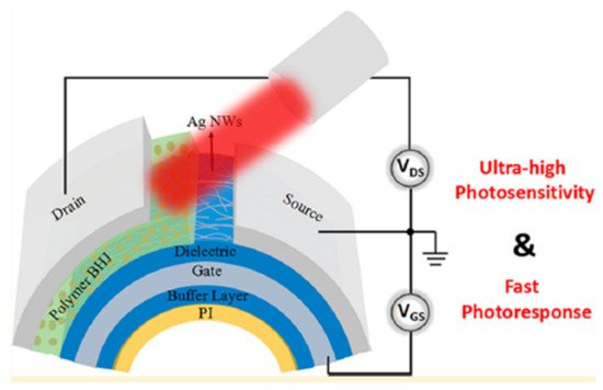
Most recently, Jiang et al. [108] developed a transistor device that comprised of an organic solar cell and a FeNi/PDMS magnetic array covered by Ag nanowires (AgNWs). Their aim was to obtain a device that could be implemented as an artificial intelligent skin (touchless human-machine interaction) or usage in optical communication. The photoactive P3HT: PCBM layer and the magnetic array part were deposited by spin-coating. When an appropriate magnetic field was applied, the magnetic array would be placed on the bottom contact. The photocurrent flowed through the device; thus, the phototransistor was in its on-state. In other words, the magnetic part acted as a gate electrode. They also fabricated the device on PET substrate to gain flexibility. It was reported that this two-terminal, solution-processed device with high on/off current ratio (~108) and fast-response would shed light on future wearable applications. Li et al. [40] studied an n-type small molecule as an active layer in BGTC OPT for the next-generation of NIR-sensitive, low-cost sensing devices. This n-type small molecule, 4,4-Difluoro-4-bora-3a,4a-diaza-s-indacene (BODIPY-BF2), was cast from solution and showed good absorbance in the NIR region (around 850 nm). They reported that annealed (θ = 90°) film (for highly ordered texture) exhibited high mobility value (µsat = 1.13 × 10⁻¹ cm2 V−1 s−1) and on/off current ratio (1.12 × 10⁶). R value was reported 1.14 × 10⁴ AW−1 at 850 nm for annealed (θ = 90°) film. The dynamic photoresponse of the device was reported stable; thus, it could have served as a good light switch. The F groups of BODIPY-BF2 could provide an O2 and/or H2O barrier property, contributing to the device stability and lifetime. A highly flexible and novel design with ultrashort channel length was demonstrated by Zhong et al. [109] for organic electronics applications in the Vis region. AgNWs were deposited on the dielectric layer, and a BHJ layer was chosen as the active layer (Figure 18). Poly[2,5-bis(alkyl) pyrrolo [3,4-c]-pyrrole-1,4(2H,5H)-dione-alt-5,5′-di(thiophen-2-yl)-2,2′-(E)-2-(2-(thiophen-2-yl) vinyl)-thiophene] (PDVT-8) and [6,6]-phenyl C61 (PC61BM) was used as the D/A. Solutions were prepared in a mixture of chloroform (CF) and chlorobenzene (CB). BHJ was spin-coated on the AgNWs network source electrode. For flexibility, a polyimide (PI) substrate was deposited by blade coating. Under 720 nm light illumination, high R (750 A W−1) and P (1 × 10⁶) values were recorded. D* was as high as 4.54 × 10¹⁵ Jones.
Figure 18. Device structure of highly flexible and novel OPT. Reprinted with permission from ref. [109]. Copyright 2018 American Chemical Society.
Solutions with different ratios of CB in the solution were prepared. The best results, e.g., lowest switch ON time of 0.72 s were achieved for 30% CB solutions. Moreover, at 30% CB concentration, the surface area of crystals was found at the highest. It was reported that 30% CB could deliver the most efficient exciton dissociation. As the bending radius went down from 54 to 18 mm, a slight decrease of R was noticed that meant the device had good mechanical stability.
Liu et al. reported [110] that a flexible, high response OPT (BGTC configuration) could be produced by the addition of a metal-ligand charge transfer (MLCT) molecule. Ruthenium complex 1 (Ru-complex 1), a photosensitizer was used to enhance responsivity and EQE value of the device by MLCT from Ru-complex 1 to the active layer which was an n-type molecule N,N′-bis(2-phenylethyl)-perylene-3,4:9,10-tetracarboxylic diimide (BPE-PTCDI). Ru-complex 1 was deposited by drop-casting. At VG = 80 V, the highest R value (7230 A W−1) and D* (1.9 × 10¹³ Jones) were obtained. The findings were attributed to electrons injection into the active component. When illumination excited Ru-1, ground state electrons were injected into the BPE-PTCDI. Ru2+ was oxidized to Ru3+, which meant holes were trapped. PI substrate was selected to obtain a mechanically flexible device for wearable organic electronic, flexible image scanners, biomedical sensing gadgets applications. In their most recent study, Lee et al. [111] used a doping agent, tris-(pentafluorophenyl)borane (BCF), to fabricate a short-wave infrared (SWIR) OPT. They spin-coated BCF-doped polytriarylamine, poly[N,N′-bis(4-butylphenyl)-N,N′-bis(phenyl) benzidine) (PolyTPD) as the gate-sensing layer in the SWIR range (λ = 1000–3200 nm) and achieved R level = 538 mA W−1 at λ = ~1500 nm and R = ~222 mA W−1 at λ = 3000 nm. When the light was exposed to the device, the gate-sensing layer absorbed the light and generated excitons. Following that, the charge separation occurred. Therefore, more holes could be induced in the P3HT active channel. The TPA units in PolyTPD acted as an electron donor and BCF molecule as acceptor. Electron transfer from PolyTPD to BCF provided the lower bandgap required to realise the SWIR absorption. It was reported that their study was a crucial step for the nextgeneration of soft electronic applications. Bilayer heterostructure (BHS) phototransistors offer high quality device design since they have BHJ layer for light absorption and exciton separation. In addition, this design has high mobility semiconductor layer for effective charge transport. Crosslinked polymeric semiconductor and BHJ bilayers were studied in a BGTC configuration to obtain a NIR light detection for imaging applications [112]. Crosslinked poly(N-alkyl diketo-pyrrolo-pyrrole dithienylthieno[3,2-b]thiophene) (PDPP-DTT) was induced on the dielectric layer as the conducting channel and BHJ (PDPP-DTT:PC61BM) as the photoactive layer by spin-coating. PDPP-TT is a low bandgap (EG = −1.2 eV) material. At 808 nm, the photoresponse characteristics exhibited that BHS OPTs had Vth shift to more positive voltages. When the device was exposed to NIR light, the drain current began to rise due to photogenerated carriers. The maximum R value was 2 × 10³ A W−1 at light intensity of 1.66 µW cm−2. By benefiting from the electron capturing of PC61BM, more photogenerated holes went from the BHJ layer to crosslinked conducting channel. This charge movement contributed to the drain current. F suitability in flexible electronics, bending studies was also conducted. It is reported that the maximum P was kept at 1 mm bending radius. It indicated that this novel OPT design could provide durability response to mechanical bending. In another study, a hybrid active layer was utilised to obtain a flexible NIR light-sensitive solution-processed OPT [113]. The hybrid layer was compromised of n-type metal oxide (In2O3)/polymer {5,5′-bis[3,5-bis(thienyl)phenyl]-2,2′-bithiophene-3-ethylesterthiophene]} (PTPBT-ET) in a BGTC structure. Polymer PTPBT-ET layer was deposited by spin-coating. In2O3 initiated fast electron transport and PTPBT-ET was used for NIR light absorbance. The study reported a good responsivity (R = 200 A W−1) and D* value (1.2 × 10¹³ Jones). Under 810 nm-NIR light, the device had high electron density, since electrons could easily jump to the conduction band of the metal oxide. As expected, the threshold voltage showed a negative shift (from 6.9 to −1.52 ± 1.21 V). A high carrier mobility (µ) of 7.10 ± 1.31 cm2 V−1 s−1 and 3.2 × 10⁷ of Ion/Ioff ratio was measured. The flexibility of the device was also examined by placing the device on a polyimide (PI) substrate and applying PMMA as the passivation layer. Despite slight distraction on NIR light absorbance, the passivation layer maintained to keep the electrical stability of the device under the 5 mm-radii bending test to 1000 cycles. They stated that the proposed design with hybrid materials has the potential in image sensors and wearable health monitoring.

3.1. Photoactivated Memory Devices and Their Applications

Studies of information storage in a friendly and flexible way have spiked significantly by the growing technological advancements. Today, keeping large amount of data with low power consumption and achievable high central processing unit rate are the top priorities of scientists. The molecular size of organic materials provides an increased storage capacity. Apart from classical ways of data storage, such as random-access memory (RAM), read-only memory (ROM), or hard disk drive (HDD), researchers have been focusing on memristors and field-effect transistor (FET)-based memory devices. The well- known frequently used gadget flash memory is also based on MOSFET-based memory. The emerge of flexible and wearable sensory devices, security, and communication technologies has encouraged explore of lightweight, soft and tailorable organic materials in three-terminal transistor memory devices, namely OFET, ferroelectric FET (FeFET) [114], and electrolyte-gated transistor (EGT) [115][116][117]. In these designs, gate electrode is the control terminal, while the transduction terminal is comprised of source and drain electrodes. When it comes to data storage, memory devices can be volatile or non-volatile [115][116]. Volatile memory keeps the stored data only if the device is fed by a continuous voltage. After removing the voltage, the memory goes back to its initial state. However, a non-volatile memory device can continue to hold the information even if the power is switched off. FET-based non-volatile memory is attained via two different mechanisms. Basically, FeFET memory devices’ working principal benefits from polarization change by using a ferroelectric dielectric layer in the transistor [118]. One of the most popular and used organic, solution-processable ferroelectric materials is poly(vinylidene fluoride) (PVDF) and a copolymer of VDF and trifluoroethylene (TrFE). This type of memory is based on dipole orientation. Another type of memory is based on charge/ion trapping [119]. Trapped charges contribute to the device in the writing and erasing process. All these processes can be interpreted by the memory window which is the Vth shifting range in the writing and erasing process and has huge importance in assessing the memory device efficiency [115][116]. P(VDF-TrFE) was used as a ferroelectric material in a TGBC, solution-processed photomemory study [120]. An alternative unit of diketopyrrolopyrrole (DPP) and thiophene-thiazolothiazole-thiophene (TzBT)- P(DPP-TzBT) was selected as a narrow bandgap semiconductor layer. P(VDF-TrFE) contributed to two additional non-volatile states compared to traditional OPTs due to polarisation of this ferroelectric material. The device showed the low resistance state “1” after applying a −100 V gate voltage in the writing process and the high resistance state “0” following the 100 V gate voltage in the erasing process. These two states retained up to 103 s which was promising for the long data storage capability. Under three different states (state 0, state 1, and 60 V gate voltage state) with 10 s light pulse-80 mW/cm2 light intensity, different photo-to-dark currents were observed. Therefore, they said that memory states could be modified by changing photo-to-dark current. When under “0” state, positive polarization occurred. That meant hole carrier density could not reach the high levels. After light illumination, free e/h pairs dissociated, giving rise to the hole carrier density. On the other hand, under “1” state, negative polarization occurred, so high hole carrier density was already induced. Higher hole carrier density was not obtained under light illumination, as it was the case in “0” state. The authors claimed that this study could shed light on information storage and flexible electronics.
Another study with both n-type and p-type materials focused on impact of dual functionality on non-volatile organic photonic transistor [121]. In this study, rod-coil material was used as the floating gate layer due to its fine functionality. The rod part was from a conjugated core and the coil part was long alkyl side chains. This material provided the necessary charge trapping. By using this material to serve as both the charge transport and memory layer, the negative effect of the energy barrier was hindered, and this led to creating a low-power consumption (0.1 V) organic photonic memory device. Threshold voltage shifting was observed in n-type (0.84 to −7.01 V, negative shift) and p-type (positive shift) behaviour. Hence, successful charge trapping and writing process was achieved. Fast programming time (<3 s) and prolonged retention time (over 104 s) demonstrated a promising new approach for photonic memory applications. Xu et al. 
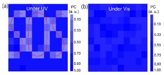
[122]. fabricated a dual-band, hybrid (organic/inorganic) active layer phototransistor by a one-step solution, suitable for secure communication applications. The organic active layer was a 2,7-dioctyl[1]-benzothieno [3,2-b][1] benzothiophene (C8-BTBT) single-crystal array and CH3NH3PbI3 NPs was the organic/ inorganic perovskite. The device presented a high R value of > 1.72 × 10⁴ A W−1 and broad absorption range (UV-Vis) in the 252–780 nm regions. The hybrid phototransistor was integrated in a matrix array (10 × 10 pixels) and performed successfully in secure communication. The C8-BTBT pattern was deposited through a shadow mask with “SOS” characters on a quartz plate, so the characters were invisible. This plate was then placed on the transistor and exposed to the light illumination. Under Vis light, no characters could be seen, since C8-BTBT had high transparency to the Vis light. On the other hand, under the UV light, the C8-BTBT absorbed the light and as the result, SOS characters appeared (Figure 19) and remained until after UV light was removed. This approach made it possible to keep information encrypted.
Figure 19. The visibility of the “SOS” characters under (a) UV light, (b) Vis light. Reprinted with permission from ref. [122]. Copyright 2019 American Chemical Society.
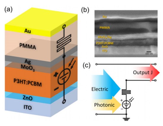
Moreover, Tzou, Cai and et al. [123] fabricated a two-terminal organic phototransistor for information technologies. Their device included a resistive random-access memory (RRAM) and an organic solar cell. They reported that the field-effect stem from their chosen integration design and the vertical two-sandwich electrode design was an excellent way for high-speed optical communication and energy saving due to the short channel in the vertical design. The photocurrent from the organic solar cell was modulated by a switchable RRAM. P3HT: PCBM, the photoactive layer was spin-coated on the top of the zinc oxide (ZnO). Ag/PMMA/Au was the structure of the RRAM (Figure 20).
Figure 20. (a) OPT device structure, (b) the cross-sectional FESEM image and (c) the equivalent circuit of the device. Reprinted with permission from ref. [123]. Copyright 2019 AIP Publishing.
The D* value of the device was calculated over 1011 Jones in the near UV-Vis range, and the rapid switch-on and switch-off characteristics of the device was detected at 2.5 kHz. The photoresponse time was 3 µs which was the best record, and the Ion/Ioff ratio 6 × 10⁴. The dual control of the device suggested a remarkable advantage to be utilized in information technology, in particular for security encryption. The electric and photonic lock could be controlled separately. In other words, when the electric lock was out of the system control, their device could be controlled by the photonic lock. This meant that the information could not be stolen by hackers. Huang et al. 
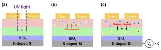
[124] reported a UV-sensing OPT device for photomemory storage and photodetectors by UV light programming/electrical erasing mechanism. Pentacene was selected as the active layer in the BGTC configuration. Below the active channel layer, doped aggregation-enhanced emission (AEE)–fluorescent electret film was deposited at various doping ratios. AEE-fluorescent triphenylamine (TPA)-based polymers (polyimide (PI) or polyamide (PA)) doped with an AEE small molecule (SM) electret was spin-coted. Electret layer emitted strong fluorescent illumination, following that pentacene could absorb fluorescent light. The photogenerated excitons were separated when VG was applied. Electrons were trapped in the electret layer; thus, hole concentration in the channel increased substantially (Figure 21).
Figure 21. Schematic diagram of programming process of OPT, (a) OPT under the UV light, (b) the photoinduced excitons in pentacene, (c) charge trapping under reverse bias. Reprinted with permission from ref. [124]. Copyright 2019 Royal Society of Chemistry.
The electrical erasing process could occur when the opposite gate voltage. Electrons were de-trapped and neutralized the holes. Their results showed memory window (MW) of 37.2 V, p value of 1.92 × 10⁶ and R being 45 A W−1 at 365 nm.
Poor charge extraction and low dissociation can limit the OPT device working in the NIR region. Low dimensional materials including quantum dots [125], nanowires [126], 2D materials [127] are reported to offer solutions for high photoconductive gain or tunable Fermi level [128]. A novel design, solution-processed graphene/organic phototransistor was reported by He et al. for a NIR region detection [129]. They realised a multifunctional device that could work both as a pulse monitoring and a photomemory. They induced electron extraction layer of ZnO on the graphene channel brought a strange approach to the device by blocking holes. Therefore, it could be switched into a photomemory device. A Graphene/ZnO/ Ternary bulk heterojunction (T-BHJ) was adopted in this novel, solution-processed OPT. T-BHJ (PTB7-Th:IEICO-4F:PC71BM) was comprised of donor (D) (poly[4,8-bis(5-(2-ethylhexyl)thiophen-2-yl) benzo[1,2-b;4,5-b′]dithiophene-2,6-diyl-alt-(4-(2-ethyl-hexyl)-3-fluorothieno[3,4b]thiophe-ne-)-2-carb-oxylate-2-6-diyl)), acceptor 1 (A1) (2,2′-((2Z,2′Z)-(((4,4,9,-9-tetrakis(4-hexylphenyl)-4,9-dihydro-sindaceno[1,2-b:5,6-b′] dithiophene2,7-diyl) bis(4-((2ethylhexyl)oxy) thiophene-5,2-diyl)) bis(methanylylidene)) bis(5,6-difluoro-3-oxo-2,3-dihydro1Hindene-2,1diylidene)) dimalononitrile) and acceptor 2 (A2) ([6,6]-phenyl C71 butyric acid methyl ester) layers. T-BHJ layer expanded the response of the device to the longer wavelengths (760–1100 nm). After NIR light illumination created excitons diffused into D and A layers and became free dissociations. ZnO blocked the holes to enter the graphene layer with the help of a deep HOMO level (−7.8 eV). Hence, recombination was prevented. The OPT exhibited a high R-value (6.1 × 10⁶ A W−1) and D* (2.4 × 10¹³ Jones). One of the main advantages of this study was to show pulse monitoring without contact in transmission mode (
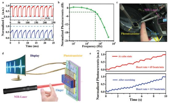
Figure 22). Figure 22c,d present remote pulse monitoring. Calm state and after 5-min exercise situation were compared and their results were correlated with physiological characteristics. These results were promising that human pulse and heart rate could be read out in real-time in a non-touching approach. Non-touched monitoring was in agreement with remote and non-invasive monitoring. Moreover, this OPT could be turned into a photomemory device with a retention time of 1000 s in the atmosphere as gate voltage of −20 V.
Figure 22. (a) normalized photocurrents of the phototransistor under light modulation, (b) normalized photocurrents as a function of modulating frequency, (c,d) the real image and the schematic of NIR-sensitive, pulse monitoring OPT sensor in transmission mode, respectively, (e) author’s pulse signals and heart rate at calm state and after exercising. Reprinted with permission from ref. [129]. Copyright 2021 John Wiley and Sons.
Furthermore, A polyimide: UV-responsive organic semiconductor 2,7-dipentyl[1]benzothieno[3,2-b][1]benzothiophene.
(PI:C5-BTBT) based, solution-processed OPT was designed [130] and investigated under different criteria, such as blending ratio effect, UV sensitivity, and electron-withdrawing groups. C5-BTBT is a small molecule that is blind to Vis but sensitive to UV-A light. The configuration of the device was BGTC, and the active layer was spin-coated at different ratios. Their results were encouraging for photomemory applications. The 70:30 blending ratio (PI:C5-BTBT) gave the highest R (429 A W−1) and p was 106, it had lower surface roughness (2.73 ± 0.4 nm) than others as PI content increased. By introducing PI, C5-BTBT grains merged. This can be explained by the reduced grain boundaries leading to higher mobility (µ = 1.00 ± 0.17 cm2 V−1 s−1). The results showed that PI:C5-BTBT blends with fast writing < 1 s, long retention times (149 s) could be preferred for the stored information applications.

3.2. Synaptic Phototransistors and Their Applications

Synaptic transistors have been widely investigated for artificial intelligence, neurological studies, and neuromorphic memory. In the human brain, when information is taken, one obeys the signal’s order to proceed. This information is then stored and processed. Synapse exists between neurons, and neurotransmitter molecules are released from pre-synaptic neurons to post-synaptic neurons. So, synaptic information begins to flow [131]. Brain-like computer systems can resemble a biological brain, and this cycle of processes can be replicated by brain-like computers [132][133]. Multi-terminal devices provide taking and reading signals simultaneously [131][134]. To mimic the human brain process, it is required to input and output data which are carried out by gate electrode (input) and source-drain electrodes (output) [135]. Synaptic transistors are devising a method where each electrode is assigned a responsibility to do. Inorganic solid electrolytes, organic solid electrolytes and inorganic-organic solid electrolytes have been applied for synaptic transistor studies as the gate dielectric layer [131][136]. Another material, poly(vinylidenefluoride-to-trifluoroethylene) (P(VDF-TrFE)) is the one of choices. One study [137] Qian et al. used P3HT as the active layer of the transistor, and the ionic liquid/P(VDF-TrFE) was considered as a hybrid electrolyte. This study was reported for artificial synapses for neuromorphic systems. Proton conductivity which is necessary for brain-like computers can be supplied by functional groups [135]. In synaptic transistors, different types of electrodes can be utilized. For instance, researchers claim that metal magnesium electrodes can reduce the biocompatibility problems because there are numerous amounts of Mg2+ ions in muscle and bone [131][138]. Electric-double layers (EDLs) are critical when the synapse space and synaptic information flow design are aimed to be occurred. This biological transmission can be mimicked by EDLs [131][139].
OFET can be enriched with a photonic memory feature by utilising a phototransistor design. Using light illumination in phototransistor sensor applications for biological synapse studies is extremely attractive, since 70–80% of the information that humans take from their environment is from visual sense. An OPT operates in a very similar to a biological system. Mobile charges in the channel are regarded as neurotransmitters. The channel conductance is named synaptic weight. Changes in synaptic, also known as synaptic plasticity weight, is regarded as a change in source-drain output current [116]. A hybrid synaptic phototransistor was designed by using solution-processed perovskite CsPbBr3/ 6,13-bis(triisopropylsilylethynyl) TIPS in a BGTC configuration [140]. CsPbBr3, the light absorption layer, was spin coated, and TIPS, conducting layer was deposited by drop-casting. Using CsPbBr3 enhanced the device photosensitivity, as pure TIPS did not high have hole sensitivity. After light illumination, the injection of photoexcited holes into the TIPS channel increased and electrons were trapped in CsPbBr3. The learning-forgetting-relearning process was examined. The learning and relearning processes took 30 and 17 pulses respectively. This behaviour resembled that of the human brain in which relearning takes less time than first-time learning. They reported light-to-dark current ratio was 1.8 × 10⁵ and R was above 2000 A W−1. High D* (2 × 10¹⁵ Jones) was achieved. These finding were specifically significant as conventional Si detectors have a D* value of nearly 4 × 10¹² Jones. It was stated that this study was very promising for future artificial visual systems.
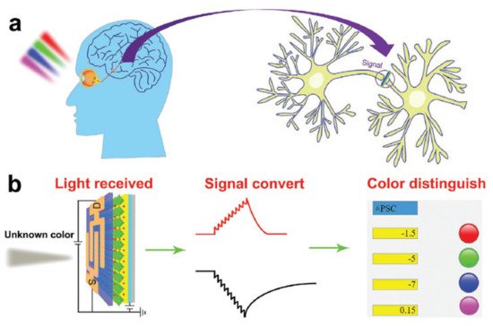
Very recently, Huang et al. reported a synaptic phototransistor (SPT) for artificial intelligence vision systems [141]. In this study, a visual system was developed to colour recognition (Figure 23). A solution-processed, 2 D Perovskite (PEA2SnI4)/Organic Heterojunction (Y6) (non-fullerene acceptor material) ambipolar synaptic phototransistor was designed. PEA2SnI4 was selected due to its non-toxic, low temperature solution processability. Because of the difficulty of colour differentiation from Vis to NIR light, they did not study only one charge carrier (only hole or only electron). This ambipolar BGTC configuration was demonstrated to sense red/green/blue colours. The photoresponse (R) of the device was a maximum of 1.83 × 10⁴ A W−1 to visible light (blue color) and 200 A W−1 to NIR light. R values of red and green colours were 9.25 × 10³ and 1.21 × 10⁴, respectively. The highest value of photosensitivity (p) value recorded was 21 to visible light (blue colour) and 3 to NIR light. p values of red and green colours were 11 and 16, respectively. NIR light was detected in positive gate voltage region that meant there was a selective detection.
Figure 23. (a) Schematic of human visual system, (b) process of light receiving, signal converting, and distinguishing of different colours. Reprinted with permission from ref. [141]. Copyright 2021 John Wiley & Sons.
Moreover, this dual-mode learning device showed that it stimulated biological neurological behaviours, such as postsynaptic current, long-term memory synaptic functions. Signal transmission in the synapse occurred as light illumination, charge trapping/detrapping in artificial studies. When the light arrived at the device, excitatory postsynaptic current (EPSC) was generated, reached its peak and then decreased slightly to lower levels. The photogenerated charges were captured at the interface, and then discharged modestly in the darkness. These findings have greatly contributed to scientific understanding of and opened exciting opportunities on mimicking the human brain and its functionalities.

References

  1. Wakayama, Y.; Hayakawa, R.; Seo, H.S. Recent progress in photoactive organic field-effect transistors. Sci. Technol. Adv. Mater. 2014, 15, 024202.
  2. Wang, C.; Zhang, X.; Hu, W. Organic photodiodes and phototransistors toward infrared detection: Materials, devices, and applications. Chem. Soc. Rev. 2020, 49, 653–670.
  3. Baeg, K.J.; Binda, M.; Natali, D.; Caironi, M.; Noh, Y.Y. Organic light detectors: Photodiodes and phototransistors. Adv. Mater. 2013, 25, 4267–4295.
  4. Xie, C.; Liu, C.K.; Loi, H.L.; Yan, F. Perovskite-Based Phototransistors and Hybrid Photodetectors. Adv. Funct. Mater. 2020, 30, 1–28.
  5. Wu, Z.; Zhai, Y.; Kim, H.; Azoulay, J.D.; Ng, T.N. Emerging Design and Characterization Guidelines for Polymer-Based Infrared Photodetectors. Acc. Chem. Res. 2018, 51, 3144–3153.
  6. Öberg, P.Å. Optical Sensors in Medical Care. Sensors Appl. 2008, 3, 15–43.
  7. Chow, P.C.Y.; Someya, T. Organic Photodetectors for Next-Generation Wearable Electronics. Adv. Mater. 2020, 32, 1–26.
  8. Zaumseil, J.; Sirringhaus, H. Electron and ambipolar transport in organic field-effect transistors. Chem. Rev. 2007, 107, 1296–1323.
  9. Xu, H.; Li, J.; Leung, B.H.K.; Poon, C.C.Y.; Ong, B.S.; Zhang, Y.; Zhao, N. A high-sensitivity near-infrared phototransistor based on an organic bulk heterojunction. Nanoscale 2013, 5, 11850–11855.
  10. Rim, Y.S.; Yang, Y.; Bae, S.H.; Chen, H.; Li, C.; Goorsky, M.S.; Yang, Y. Ultrahigh and Broad Spectral Photodetectivity of an Organic-Inorganic Hybrid Phototransistor for Flexible Electronics. Adv. Mater. 2015, 27, 6885–6891.
  11. García De Arquer, F.P.; Armin, A.; Meredith, P.; Sargent, E.H. Solution-processed semiconductors for next-generation photodetectors. Nat. Rev. Mater. 2017, 2, 1–17.
  12. Liu, J.; Wang, Y.; Wen, H.; Bao, Q.; Shen, L.; Ding, L. Organic Photodetectors: Materials, Structures, and Challenges. Sol. RRL 2020, 4, 1–8.
  13. Nasiri, N.; Bo, R.; Wang, F.; Fu, L.; Tricoli, A. Ultraporous Electron-Depleted ZnO Nanoparticle Networks for Highly Sensitive Portable Visible-Blind UV Photodetectors. Adv. Mater. 2015, 27, 4336–4343.
  14. Kurz, W.; Yetisen, A.K.; Kaito, M.V.; Fuchter, M.J.; Jakobi, M.; Elsner, M.; Koch, A.W. UV-Sensitive Wearable Devices for Colorimetric Monitoring of UV Exposure. Adv. Opt. Mater. 2020, 8, 1901969.
  15. Xu, H.; Liu, J.; Zhang, J.; Zhou, G.; Luo, N.; Zhao, N. Flexible Organic/Inorganic Hybrid Near-Infrared Photoplethysmogram Sensor for Cardiovascular Monitoring. Adv. Mater. 2017, 29, 1–6.
  16. Li, N.; Lan, Z.; Lau, Y.S.; Xie, J.; Zhao, D.; Zhu, F. SWIR Photodetection and Visualization Realized by Incorporating an Organic SWIR Sensitive Bulk Heterojunction. Adv. Sci. 2020, 7, 2000444.
  17. Lee, Y.H.; Jang, M.; Lee, M.Y.; Kweon, O.Y.; Oh, J.H. Flexible Field-Effect Transistor-Type Sensors Based on Conjugated Molecules. Chem 2017, 3, 724–763.
  18. Gu, P.; Yao, Y.; Feng, L.; Niu, S.; Dong, H. Recent advances in polymer phototransistors. Polym. Chem. 2015, 6, 7933–7944.
  19. Dou, L.; Liu, Y.; Hong, Z.; Li, G.; Yang, Y. Low-Bandgap Near-IR Conjugated Polymers/Molecules for Organic Electronics. Chem. Rev. 2015, 115, 12633–12665.
  20. Mei, J.; Diao, Y.; Appleton, A.L.; Fang, L.; Bao, Z. Integrated materials design of organic semiconductors for field-effect transistors. J. Am. Chem. Soc. 2013, 135, 6724–6746.
  21. Guo, Y.; Yu, G.; Liu, Y. Functional organic field-effect transistors. Adv. Mater. 2010, 22, 4427–4447.
  22. Chortos, A.; Liu, J.; Bao, Z. Pursuing prosthetic electronic skin. Nat. Mater. 2016, 15, 937–950.
  23. Serdar Sariciftci, N. Plastic photovoltaic devices. Mater. Today 2004, 7, 36–40.
  24. Liu, J.; Jiang, L.; Shi, J.; Li, C.; Shi, Y.; Tan, J.; Li, H.; Jiang, H.; Hu, Y.; Liu, X.; et al. Relieving the Photosensitivity of Organic Field-Effect Transistors. Adv. Mater. 2020, 32, 1–8.
  25. Huang, J.; Du, J.; Cevher, Z.; Ren, Y.; Wu, X.; Chu, Y. Printable and Flexible Phototransistors Based on Blend of Organic Semiconductor and Biopolymer. Adv. Funct. Mater. 2017, 27, 1–8.
  26. Park, H.L.; Kim, M.H.; Kim, H. Improvement of photoresponse in organic phototransistors through bulk effect of photoresponsive gate insulators. Materials 2020, 13, 1565.
  27. Huang, X.; Ji, D.; Fuchs, H.; Hu, W.; Li, T. Recent Progress in Organic Phototransistors: Semiconductor Materials, Device Structures and Optoelectronic Applications. ChemPhotoChem 2020, 4, 9–38.
  28. Horowitz, B.G. Organic Field-Effect Transistors. Adv. Mater. 1998, 10, 365–377.
  29. Braga, D.; Horowitz, G. High-Performance organic field-effect transistors. Adv. Mater. 2009, 21, 1473–1486.
  30. Sirringhaus, H. Device physics of solution-processed organic field-effect transistors. Adv. Mater. 2005, 17, 2411–2425.
  31. Sirringhaus, H. 25th anniversary article: Organic field-effect transistors: The path beyond amorphous silicon. Adv. Mater. 2014, 26, 1319–1335.
  32. Yang, S.Y.; Shin, K.; Park, C.E. The effect of gate-dielectric surface energy on pentacene morphology and organic field-effect transistor characteristics. Adv. Funct. Mater. 2005, 15, 1806–1814.
  33. Ren, X.; Yang, F.; Gao, X.; Cheng, S.; Zhang, X.; Dong, H.; Hu, W. Organic Field-Effect Transistor for Energy-Related Applications: Low-Power-Consumption Devices, Near-Infrared Phototransistors, and Organic Thermoelectric Devices. Adv. Energy Mater. 2018, 8, 1–27.
  34. Han, H.; Lee, C.; Kim, H.; Kim, Y. Flexible Near-Infrared Plastic Phototransistors with Conjugated Polymer Gate-Sensing Layers. Adv. Funct. Mater. 2018, 28, 1–8.
  35. Park, J.; Kim, H.; Kim, T.; Lee, C.; Song, D.I.; Kim, Y. Effect of top channel thickness in near infrared organic phototransistors with conjugated polymer gate-sensing layers. Electronics 2019, 8, 1493.
  36. Lei, Y.; Li, N.; Chan, W.K.E.; Ong, B.S.; Zhu, F. Highly sensitive near infrared organic phototransistors based on conjugated polymer nanowire networks. Org. Electron. 2017, 48, 12–18.
  37. Lee, G.H.; Moon, H.; Kim, H.; Lee, G.H.; Kwon, W.; Yoo, S.; Myung, D.; Yun, S.H.; Bao, Z.; Hahn, S.K. Multifunctional materials for implantable and wearable photonic healthcare devices. Nat. Rev. Mater. 2020, 5, 149–165.
  38. Li, N.; Lei, Y.; Chan, W.K.E.; Zhu, F. Broadband phototransistors realised by incorporating a bi-layer perovskite/NIR light absorbing polymer channel. J. Mater. Chem. C 2019, 7, 4808–4816.
  39. Xia, Y.; Wang, L.; Deng, X.; Li, D.; Zhu, X.; Cao, Y. Photocurrent response wavelength up to 1.1 μm from photovoltaic cells based on narrow-band-gap conjugated polymer and fullerene derivative. Appl. Phys. Lett. 2006, 89, 89–92.
  40. Li, F.; Chen, Y.; Ma, C.; Buttner, U.; Leo, K.; Wu, T. High-Performance Near-Infrared Phototransistor Based on n-Type Small-Molecular Organic Semiconductor. Adv. Electron. Mater. 2017, 3, 1600430.
  41. Ebisawa, F.; Kurokawa, T.; Nara, S. Electrical properties of polyacetylene/polysiloxane interface. J. Appl. Phys. 1983, 54, 3255–3259.
  42. Wang, C.; Dong, H.; Hu, W.; Liu, Y.; Zhu, D. Semiconducting π-Conjugated Systems in Field-Effect Transistors. Chem. Rev. 2012, 112, 2208–2267.
  43. Fratini, S.; Nikolka, M.; Salleo, A.; Schweicher, G.; Sirringhaus, H. Charge transport in high-mobility conjugated polymers and molecular semiconductors. Nat. Mater. 2020, 19, 491–502.
  44. Shi, L.; Liang, Q.; Wang, W.; Zhang, Y.; Li, G.; Ji, T.; Hao, Y.; Cui, Y. Research progress in organic photomultiplication photodetectors. Nanomaterials 2018, 8, 713.
  45. Xie, W.; Menke, S.M.; Frisbie, C.D.; Holmes, R.J. Experimental Characterization of Charge and Exciton Transport in Organic Semiconductors. WSPC Ref. Org. Electron. Org. Semicond. 2016, 1, 231–291.
  46. Forrest, S.R.; Thompson, M.E. Introduction: Organic electronics and optoelectronics. Chem. Rev. 2007, 107, 923–925.
  47. Rivnay, J.; Inal, S.; Salleo, A.; Owens, R.M.; Berggren, M.; Malliaras, G.G. Organic electrochemical transistors. Nat. Rev. Mater. 2018, 3, 17086.
  48. Russ, B.; Glaudell, A.; Urban, J.J.; Chabinyc, M.L.; Segalman, R.A. Organic thermoelectric materials for energy harvesting and temperature control. Nat. Rev. Mater. 2016, 1, 16050.
  49. van de Burgt, Y.; Melianas, A.; Keene, S.T.; Malliaras, G.; Salleo, A. Organic electronics for neuromorphic computing. Nat. Electron. 2018, 1, 386–397.
  50. Schlesinger, R. Chapter 2—Fundamentals. In Energy-Level Control at Hybrid Inorganic/Organic Semiconductor Interfaces, 1st ed.; Springer Theses; Springer International Publishing: Berlin/Heidelberg, Germany, 2017; pp. 7–45. ISBN 9783319466248.
  51. Kalyani, N.T.; Swart, H.; Dhoble, S.J. Luminescence in Organic Semiconductors. In Principles and Applications of Organic Light Emitting Diodes (OLEDs); Elsevier: Amsterdam, The Netherlands, 2017; pp. 39–64. ISBN 9780081012130.
  52. Nunzi, J.-M. Organic Materials and Devices for Photovoltaic Applicaitons. Photovolt. Photoactive Mater. Prop. Technol. Appl. Kluwer Acad. Publ. 2002, 3, 197–224.
  53. Sturge, M.D. Electrons and Holes in Semiconductors. Stat. Therm. Phys. 2020, 269–290.
  54. Brütting, W. Physics of Organic Semiconductors, 1st ed.; Wiley-VCH Verlag GmbH & Co. KGaA: Weinheim, Germany, 2006; ISBN 352740550X.
  55. Zhu, M.; Lv, S.; Wang, Q.; Zhang, G.; Lu, H.; Qiu, L. Enhanced near-infrared photoresponse of organic phototransistors based on single-component donor-acceptor conjugated polymer nanowires. Nanoscale 2016, 8, 7738–7748.
  56. Nam, S.; Han, H.; Seo, J.; Song, M.; Kim, H.; Anthopoulos, T.D.; McCulloch, I.; Bradley, D.D.C.; Kim, Y. Ambipolar Organic Phototransistors with p-Type/n-Type Conjugated Polymer Bulk Heterojunction Light-Sensing Layers. Adv. Electron. Mater. 2016, 2, 1–8.
  57. Zhang, F.; Qu, G.; Mohammadi, E.; Mei, J.; Diao, Y. Solution-Processed Nanoporous Organic Semiconductor Thin Films: Toward Health and Environmental Monitoring of Volatile Markers. Adv. Funct. Mater. 2017, 27, 17–20.
  58. RAO, M.C.; Shekhawat, M.S. A Brief Survey on Basic Properties of Thin Films for Device Application. Int. J. Mod. Phys. Conf. Ser. 2013, 22, 576–582.
  59. Huang, W.; Feng, L.; Wang, G.; Reichmanis, E. Wearable Organic Nano-sensors. In Flexible and Wearable Electronics for Smart Clothing, 1st ed.; Wiley-VCH Verlag GmbH & Co. KGaA.: Hoboken, NJ, USA, 2020; pp. 1–27.
  60. Street, R.A. Thin-Film Transistors. Adv. Mater. 2009, 21, 2007–2022.
  61. Ong, B.S.; Wu, Y.; Liu, P.; Gardner, S. High-Performance Semiconducting Polythiophenes for Organic Thin-Film Transistors. J. Am. Chem. Soc. 2004, 126, 3378–3379.
  62. Torsi, L.; Magliulo, M.; Manoli, K.; Palazzo, G. Organic field-effect transistor sensors: A tutorial review. Chem. Soc. Rev. 2013, 42, 8612–8628.
  63. Li, H.; Shi, W.; Dailey, J.; Jang, H.-J.; Song, J.; Yu, J.; Katz, H.E. Vapor Sensing Using Organic, Polymer, and Nanomaterial Field-Effect Transistors, 2nd ed.; Elsevier: Amsterdam, The Netherlands, 2019; ISBN 9780081022849.
  64. Park, S.J.; Lee, S.H.; Yang, H.; Park, C.S.; Lee, C.S.; Kwon, O.S.; Park, T.H.; Jang, J. Human Dopamine Receptor-Conjugated Multidimensional Conducting Polymer Nanofiber Membrane for Dopamine Detection. ACS Appl. Mater. Interfaces 2016, 8, 28897–28903.
  65. Someya, T.; Dodabalapur, A.; Huang, J.; See, K.C.; Katz, H.E. Chemical and Physical Sensing by Organic Field-Effect Transistors and Related Devices. Adv. Mater. 2010, 22, 3799–3811.
  66. Hu, J.; Wei, W.; Ke, S.; Zeng, X.; Lin, P. A novel and sensitive sarcosine biosensor based on organic electrochemical transistor. Electrochim. Acta 2019, 307, 100–106.
  67. Zhu, H.; Luo, W.; Ciesielski, P.N.; Fang, Z.; Zhu, J.Y.; Henriksson, G.; Himmel, M.E.; Hu, L. Wood-Derived Materials for Green Electronics, Biological Devices, and Energy Applications. Chem. Rev. 2016, 116, 9305–9374.
  68. Huang, J.; Zhu, H.; Chen, Y.; Preston, C.; Rohrbach, K.; Cumings, J.; Hu, L. Highly transparent and flexible nanopaper transistors. ACS Nano 2013, 7, 2106–2113.
  69. Tobjörk, D.; Österbacka, R. Paper electronics. Adv. Mater. 2011, 23, 1935–1961.
  70. Qian, C.; Sun, J.; Yang, J.; Gao, Y. Flexible organic field-effect transistors on biodegradable cellulose paper with efficient reusable ion gel dielectrics. RSC Adv. 2015, 5, 14567–14574.
  71. Kleemann, H.; Krechan, K.; Fischer, A.; Leo, K. A Review of Vertical Organic Transistors. Adv. Funct. Mater. 2020, 30, 1907113.
  72. Mohammadian, N.; Faraji, S.; Sagar, S.; Das, B.C.; Turner, M.L.; Majewski, L.A. One-volt, solution-processed organic transistors with self-assembled monolayer-Ta2O5 gate dielectrics. Materials 2019, 12, 2563.
  73. Seck, M.; Mohammadian, N.; Diallo, A.K.; Faraji, S.; Saadi, M.; Erouel, M.; Ly, E.H.B.; Khirouni, K.; Majewski, L.A. Low voltage organic transistors with water-processed gum arabic dielectric. Synth. Met. 2020, 267, 116447.
  74. Lucas, B.; Trigaud, T.; Videlot-Ackermann, C. Organic transistors and phototransistors based on small molecules. Polym. Int. 2012, 61, 374–389.
  75. Ortiz, R.P.; Facchetti, A.; Marks, T.J. High-k organic, inorganic, and hybrid dielectrics for low-voltage organic field-effect transistors. Chem. Rev. 2010, 110, 205–239.
  76. Chen, X.; Zhang, H.; Zhang, Y.; Guan, X.; Zhang, Z.; Chen, D. Low-power flexible organic field-effect transistors with solution-processable polymer-ceramic nanoparticle composite dielectrics. Nanomaterials 2020, 10, 518.
  77. Faraji, S.; Danesh, E.; Tate, D.J.; Turner, M.L.; Majewski, L.A. Cyanoethyl cellulose-based nanocomposite dielectric for low-voltage, solution-processed organic field-effect transistors (OFETs). J. Phys. D Appl. Phys. 2016, 49, 185102.
  78. Faraji, S.; Hashimoto, T.; Turner, M.L.; Majewski, L.A. Solution-processed nanocomposite dielectrics for low voltage operated OFETs. Org. Electron. 2015, 17, 178–183.
  79. Gao, Y.; Yi, Y.; Wang, X.; Meng, H.; Lei, D.; Yu, X.F.; Chu, P.K.; Li, J. A Novel Hybrid-Layered Organic Phototransistor Enables Efficient Intermolecular Charge Transfer and Carrier Transport for Ultrasensitive Photodetection. Adv. Mater. 2019, 31, 1–9.
  80. Carr, J.A.; Chaudhary, S. The identification, characterization and mitigation of defect states in organic photovoltaic devices: A review and outlook. Energy Environ. Sci. 2013, 6, 3414–3438.
  81. Lee, H.; Ahn, J.; Im, S.; Kim, J.; Choi, W. High-Responsivity Multilayer MoSe2 Phototransistors with Fast Response Time. Sci. Rep. 2018, 8, 1–8.
  82. Pesavento, P.V.; Chesterfield, R.J.; Newman, C.R.; Frisble, C.D. Gated four-probe measurements on pentacene thin-film transistors: Contact resistance as a function of gate voltage and temperature. J. Appl. Phys. 2004, 96, 7312–7324.
  83. Kymissis, I.; Dimitrakopoulos, C.D.; Purushothaman, S. High-Performance Bottom Electrode Organic. IEEE Trans. Electron Devices 2001, 48, 1060–1064.
  84. Eggers, H.; Schackmar, F.; Abzieher, T.; Sun, Q.; Lemmer, U.; Vaynzof, Y.; Richards, B.S.; Hernandez-Sosa, G.; Paetzold, U.W. Inkjet-Printed Micrometer-Thick Perovskite Solar Cells with Large Columnar Grains. Adv. Energy Mater. 2020, 10, 1903184.
  85. Corzo, D.; Almasabi, K.; Bihar, E.; Macphee, S.; Rosas-Villalva, D.; Gasparini, N.; Inal, S.; Baran, D. Digital Inkjet Printing of High-Efficiency Large-Area Nonfullerene Organic Solar Cells. Adv. Mater. Technol. 2019, 4, 1900040.
  86. Tang, W.; Huang, Y.; Han, L.; Liu, R.; Su, Y.; Guo, X.; Yan, F. Recent progress in printable organic field effect transistors. J. Mater. Chem. C 2019, 7, 790–808.
  87. Feng, L.; Jiang, C.; Ma, H.; Guo, X.; Nathan, A. All ink-jet printed low-voltage organic field-effect transistors on flexible substrate. Org. Electron. 2016, 38, 186–192.
  88. Perinot, A.; Passarella, B.; Giorgio, M.; Caironi, M. Walking the Route to GHz Solution-Processed Organic Electronics: A HEROIC Exploration. Adv. Funct. Mater. 2020, 30, 1907641.
  89. Yokota, T.; Sekitani, T.; Kato, Y.; Kuribara, K.; Zschieschang, U.; Klauk, H.; Yamamoto, T.; Takimiya, K.; Kuwabara, H.; Ikeda, M.; et al. Low-voltage organic transistor with subfemtoliter inkjet source–drain contacts. MRS Commun. 2011, 1, 3–6.
  90. Sele, C.W.; von Werne, T.; Friend, R.H.; Sirringhaus, H. Lithography-Free, Self-Aligned Inkjet Printing with Sub-Hundred-Nanometer Resolution. Adv. Mater. 2005, 17, 997–1001.
  91. Huang, Y.; Tang, W.; Chen, S.; Han, L.; Hou, X.; Guo, X. Scalable Processing of Low Voltage Organic Field Effect Transistors With a Facile Soft-Contact Coating Approach. IEEE Electron Device Lett. 2019, 40, 1945–1948.
  92. Duan, S.; Wang, T.; Geng, B.; Gao, X.; Li, C.; Zhang, J.; Xi, Y.; Zhang, X.; Ren, X.; Hu, W. Solution-Processed Centimeter-Scale Highly Aligned Organic Crystalline Arrays for High-Performance Organic Field-Effect Transistors. Adv. Mater. 2020, 32, 1–8.
  93. Yao, Y.; Zhang, L.; Leydecker, T.; Samorì, P. Direct Photolithography on Molecular Crystals for High Performance Organic Optoelectronic Devices. J. Am. Chem. Soc. 2018, 140, 6984–6990.
  94. Zhang, Z.; Peng, B.; Ji, X.; Pei, K.; Chan, P.K.L. Marangoni-Effect-Assisted Bar-Coating Method for High-Quality Organic Crystals with Compressive and Tensile Strains. Adv. Funct. Mater. 2017, 27, 1703443.
  95. Singh, A.K.; Chourasia, N.K.; Pal, B.N.; Pandey, A.; Chakrabarti, P. Low Operating Voltage Solution Processed (Li2ZnO2) Dielectric and (SnO2) Channel-Based Medium Wave UV-B Phototransistor for Application in Phototherapy. IEEE Trans. Electron Devices 2020, 67, 2028–2034.
  96. Santiago, I. Trends and Innovations in Biosensors for COVID-19 Mass Testing. ChemBioChem 2020, 21, 2880–2889.
  97. Choi, J.R. Development of Point-of-Care Biosensors for COVID-19. Front. Chem. 2020, 8, 517.
  98. Asif, M.; Ajmal, M.; Ashraf, G.; Muhammad, N.; Aziz, A.; Iftikhar, T.; Wang, J.; Liu, H. The role of biosensors in coronavirus disease-2019 outbreak. Curr. Opin. Electrochem. 2020, 23, 174–184.
  99. Şahin, S.; Ünlü, C.; Trabzon, L. Affinity biosensors developed with quantum dots in microfluidic systems. Emerg. Mater. 2021, 4, 1–23.
  100. Lee, I.; Park, N.; Lee, H.; Hwang, C.; Kim, J.H.; Park, S. Systematic review on human skin-compatible wearable photoplethysmography sensors. Appl. Sci. 2021, 11, 2313.
  101. Parak, J.; Korhonen, I. Evaluation of wearable consumer heart rate monitors based on photopletysmography. In Proceedings of the 36th Annual International Conference of the IEEE Engineering in Medicine and Biology Society, Chicago, IL, USA, 26–30 August 2014; pp. 3670–3673.
  102. Rozi, R.M.; Usman, S.; Mohd Ali, M.A.; Reaz, M.B.I. Second Derivatives of Photoplethysmography (PPG) for Estimating Vascular Aging of Atherosclerotic Patients. In Proceedings of the 2012 IEEE-EMBS Conference on Biomedical Engineering and Sciences, Langkawi, Malaysia, 17–19 December 2012; pp. 256–259.
  103. Beachey, W. Respiratory Care Anatomy and Physiology: Foundations for Clinical Practice, 2nd ed.; Mosby Elsevier: St. Louis, MO, USA, 2007.
  104. Lee, H.; Ko, H.; Lee, J. Reflectance pulse oximetry: Practical issues and limitations. ICT Express 2016, 2, 195–198.
  105. Lauterbach, C.J.; Romano, P.A.; Greisler, L.A.; Brindle, R.A.; Ford, K.R.; Kuennen, M.R. Accuracy and Reliability of Commercial Wrist-Worn Pulse Oximeter During Normobaric Hypoxia Exposure Under Resting Conditions. Res. Q. Exerc. Sport 2020, 92, 549–558.
  106. Nitzan, M.; Romem, A.; Koppel, R. Pulse oximetry: Fundamentals and technology update. Med. Devices Evid. Res. 2014, 7, 231–239.
  107. Tao, J.; Liu, D.; Qin, Z.; Shao, B.; Jing, J.; Li, H.; Dong, H.; Xu, B.; Tian, W. Organic UV-Sensitive Phototransistors Based on Distriphenylamineethynylpyrene Derivatives with Ultra-High Detectivity Approaching 1018. Adv. Mater. 2020, 32, 1–9.
  108. Jiang, C.Y.; Tsai, C.H.; Tzou, C.Y.; Hsu, F.C.; Chen, Y.F. Magnetically controllable and flexible phototransistor for artificial intelligent skin with additional perception. Org. Electron. 2020, 85, 105849.
  109. Zhong, J.; Wu, X.; Lan, S.; Fang, Y.; Chen, H.; Guo, T. High Performance Flexible Organic Phototransistors with Ultrashort Channel Length. ACS Photonics 2018, 5, 3712–3722.
  110. Liu, X.; Lee, E.K.; Kim, D.Y.; Yu, H.; Oh, J.H. Flexible Organic Phototransistor Array with Enhanced Responsivity via Metal-Ligand Charge Transfer. ACS Appl. Mater. Interfaces 2016, 8, 7291–7299.
  111. Lee, C.; Kim, H.; Kim, Y. Short-wave infrared organic phototransistors with strong infrared-absorbing polytriarylamine by electron-transfer doping. NPJ Flex. Electron. 2021, 5, 1–9.
  112. Li, Q.; Ran, Y.; Shi, W.; Qin, M.; Sun, Y.; Kuang, J.; Wang, H.; Chen, H.; Guo, Y.; Liu, Y. High-performance near-infrared polymeric phototransistors realized by combining cross-linked polymeric semiconductors and bulk heterojunction bilayer structures. Appl. Mater. Today 2021, 22, 100899.
  113. Li, D.; Du, J.; Tang, Y.; Liang, K.; Wang, Y.; Ren, H.; Wang, R.; Meng, L.; Zhu, B.; Li, Y. Flexible and Air-Stable Near-Infrared Sensors Based on Solution-Processed Inorganic–Organic Hybrid Phototransistors. Adv. Funct. Mater. 2021, 31, 1–10.
  114. Kim, M.-K.; Lee, J.-S. Ferroelectric Analog Synaptic Transistors. Nano Lett. 2019, 19, 2044–2050.
  115. Zhu, Z.; Guo, Y.; Liu, Y. Application of organic field-effect transistors in memory. Mater. Chem. Front. 2020, 4, 2845–2862.
  116. Yu, Y.; Ma, Q.; Ling, H.; Li, W.; Ju, R.; Bian, L.; Shi, N.; Qian, Y.; Yi, M.; Xie, L.; et al. Small-Molecule-Based Organic Field-Effect Transistor for Nonvolatile Memory and Artificial Synapse. Adv. Funct. Mater. 2019, 29, 1–31.
  117. Gao, S.; Yi, X.; Shang, J.; Liu, G.; Li, R.-W. Organic and hybrid resistive switching materials and devices. Chem. Soc. Rev. 2019, 48, 1531–1565.
  118. Wang, H.; Zhao, Q.; Ni, Z.; Li, Q.; Liu, H.; Yang, Y.; Wang, L.; Ran, Y.; Guo, Y.; Hu, W.; et al. A Ferroelectric/Electrochemical Modulated Organic Synapse for Ultraflexible, Artificial Visual-Perception System. Adv. Mater. 2018, 30, e1803961.
  119. Wang, Z.; Zhang, S.-R.; Zhou, L.; Mao, J.-Y.; Han, S.-T.; Ren, Y.; Yang, J.-Q.; Wang, Y.; Zhai, Y.; Zhou, Y. Functional Non-Volatile Memory Devices: From Fundamentals to Photo-Tunable Properties. Phys. Status Solidi—Rapid Res. Lett. 2019, 13, 1800644.
  120. Zhao, Q.; Wang, H.; Jiang, L.; Zhen, Y.; Dong, H.; Hu, W. Solution-Processed Flexible Organic Ferroelectric Phototransistor. ACS Appl. Mater. Interfaces 2017, 9, 43880–43885.
  121. Chiang, Y.C.; Hung, C.C.; Lin, Y.C.; Chiu, Y.C.; Isono, T.; Satoh, T.; Chen, W.C. High-Performance Nonvolatile Organic Photonic Transistor Memory Devices using Conjugated Rod–Coil Materials as a Floating Gate. Adv. Mater. 2020, 32, 1–8.
  122. Xu, X.; Deng, W.; Zhang, X.; Huang, L.; Wang, W.; Jia, R.; Wu, D.; Zhang, X.; Jie, J.; Lee, S.T. Dual-Band, High-Performance Phototransistors from Hybrid Perovskite and Organic Crystal Array for Secure Communication Applications. ACS Nano 2019, 13, 5910–5919.
  123. Tzou, C.Y.; Cai, S.Y.; Tseng, C.Y.; Chang, C.Y.; Chiang, S.Y.; Jiang, C.Y.; Li, Y.H.; Ma, J.M.; Liao, Y.M.; Hsu, F.C.; et al. An ultra-fast two-terminal organic phototransistor with vertical topology for information technologies. Appl. Phys. Lett. 2019, 114, 193301.
  124. Huang, T.Y.; Chen, C.H.; Lin, C.C.; Lee, Y.J.; Liu, C.L.; Liou, G.S. UV-sensing organic phototransistor memory devices with a doped organic polymer electret composed of triphenylamine-based aggregation-induced emission luminogens. J. Mater. Chem. C 2019, 7, 11014–11021.
  125. Medintz, I.L.; Uyeda, H.T.; Goldman, E.R.; Mattoussi, H. Quantum dot bioconjugates for imaging, labelling and sensing. Nat. Mater. 2005, 4, 435–446.
  126. Hu, J.; Odom, T.W.; Lieber, C.M. Chemistry and Physics in One Dimension: Synthesis and Properties of Nanowires and Nanotubes. Acc. Chem. Res. 1999, 32, 435–445.
  127. Novoselov, K.S.; Jiang, D.; Schedin, F.; Booth, T.J.; Khotkevich, V.V.; Morozov, S.V.; Geim, A.K. Two-dimensional atomic crystals. Proc. Natl. Acad. Sci. USA 2005, 102, 10451–10453.
  128. Fang, H.; Hu, W. Photogating in Low Dimensional Photodetectors. Adv. Sci. 2017, 4, 1700323.
  129. He, Z.; Han, J.; Du, X.; Cao, L.; Wang, J.; Zheng, C.; Lin, H.; Tao, S. Photomemory and Pulse Monitoring Featured Solution-Processed Near-Infrared Graphene/Organic Phototransistor with Detectivity of 2.4 × 10¹³ Jones. Adv. Funct. Mater. 2021, 31, 1–8.
  130. Ljubic, D.; Liu, W.; González-Espinoza, C.E.; Hu, N.-X.; Wu, Y.; Zhu, S. Binary Blends of Polyimide and Benzothienobenzothiophene for High-Performance Solution-Processed Organic Phototransistors. Adv. Electron. Mater. 2017, 3, 1700284.
  131. Li, J.; Fu, W.H.; Li, L.K.; Jiang, D.L.; He, L.C.; Zhu, W.Q.; Zhang, J.H. Recent advances in solid electrolytes for synaptic transistors. Org. Electron. 2021, 95, 106196.
  132. Yoon, C.; Lee, J.H.; Lee, S.; Jeon, J.H.; Jang, J.T.; Kim, D.H.; Kim, Y.H.; Park, B.H. Synaptic Plasticity Selectively Activated by Polarization-Dependent Energy-Efficient Ion Migration in an Ultrathin Ferroelectric Tunnel Junction. Nano Lett. 2017, 17, 1949–1955.
  133. Lu, K.; Li, X.; Sun, Q.; Pang, X.; Chen, J.; Minari, T.; Liu, X.; Song, Y. Solution-processed electronics for artificial synapses. Mater. Horiz. 2021, 8, 447–470.
  134. Wan, C.J.; Liu, Y.H.; Zhu, L.Q.; Feng, P.; Shi, Y.; Wan, Q. Short-Term Synaptic Plasticity Regulation in Solution-Gated Indium–Gallium–Zinc-Oxide Electric-Double-Layer Transistors. ACS Appl. Mater. Interfaces 2016, 8, 9762–9768.
  135. Yang, Y.; Wen, J.; Guo, L.; Wan, X.; Du, P.; Feng, P.; Shi, Y.; Wan, Q. Long-Term Synaptic Plasticity Emulated in Modified Graphene Oxide Electrolyte Gated IZO-Based Thin-Film Transistors. ACS Appl. Mater. Interfaces 2016, 8, 30281–30286.
  136. Yang, J.-T.; Ge, C.; Du, J.-Y.; Huang, H.-Y.; He, M.; Wang, C.; Lu, H.-B.; Yang, G.-Z.; Jin, K.-J. Artificial Synapses Emulated by an Electrolyte-Gated Tungsten-Oxide Transistor. Adv. Mater. 2018, 30, 1801548.
  137. Qian, C.; Sun, J.; Kong, L.; Gou, G.; Yang, J.; He, J.; Gao, Y.; Wan, Q. Artificial Synapses Based on in-Plane Gate Organic Electrochemical Transistors. ACS Appl. Mater. Interfaces 2016, 8, 26169–26175.
  138. Raeis-Hosseini, N.; Park, Y.; Lee, J.-S. Flexible Artificial Synaptic Devices Based on Collagen from Fish Protein with Spike-Timing-Dependent Plasticity. Adv. Funct. Mater. 2018, 28, 1800553.
  139. Nawrocki, R.A.; Voyles, R.M.; Shaheen, S.E. A Mini Review of Neuromorphic Architectures and Implementations. IEEE Trans. Electron Devices 2016, 63, 3819–3829.
  140. Liu, J.; Yang, Z.; Gong, Z.; Shen, Z.; Ye, Y.; Yang, B.; Qiu, Y.; Ye, B.; Xu, L.; Guo, T.; et al. Weak Light-Stimulated Synaptic Hybrid Phototransistors Based on Islandlike Perovskite Films Prepared by Spin Coating. ACS Appl. Mater. Interfaces 2021, 13, 13362–13371.
  141. Huang, X.; Li, Q.; Shi, W.; Liu, K.; Zhang, Y.; Liu, Y.; Wei, X.; Zhao, Z.; Guo, Y.; Liu, Y. Dual-Mode Learning of Ambipolar Synaptic Phototransistor Based on 2D Perovskite/Organic Heterojunction for Flexible Color Recognizable Visual System. Small 2021, 17, 1–8.
More
Information
Contributor MDPI registered users' name will be linked to their SciProfiles pages. To register with us, please refer to https://encyclopedia.pub/register :
View Times: 1.2K
Revisions: 2 times (View History)
Update Date: 27 Jan 2022
1000/1000