Crystal defects play roles in wide bandgap semiconductors and dielectrics under extreme environments (high temperature, high electric and magnetic fields, intense radiation, and mechanical stresses) found in power electronics. Defects requires real-time in situ material characterization during material synthesis and when the material is subjected to extreme environmental stress. It is shown that the reduction of defects represents a fundamental breakthrough that will enable wide bandgap (WBG) semiconductors to reach full potential. High-brightness X-rays from synchrotron sources and advanced electron microscopy techniques are used for atomic-level material probing to understand and optimize the genesis and movement of crystal defects during material synthesis and extreme environmental stress.
1. Introduction
One of the most significant challenges for materials technology in the 21st century pertains to the excited state characteristics of crystal defects present in semiconductor and dielectric materials used for energy conversion devices
[1][2][3][4]. These high-voltage and high-power switching devices experience extreme electrical and thermal stresses because of inherent high electric fields and high currents generated during their operation. In addition, they are subjected to extreme environments, including high ambient temperatures, thermal cycles, high magnetic fields, radiation, vibration, and corrosion.
Silicon has served well as the industry “workhorse” semiconductor for power electronics switching applications; however, wide bandgap (WBG) semiconductors, especially diamond and GaN, with significantly superior electrical and thermal characteristics compared to silicon, are the key enablers for transforming the electricity infrastructure for the 21st century
[3][4][5][6]. Current filament formation and micro plasma generation are the main causes of power semiconductor device failures in circuit applications. Device failures occur either during the on-state when conducting high amounts of currents or when switching high voltages and currents. There are significant experimental test results suggesting that material defects in WBG semiconductors and diamond severely limit the manufacturing yield, device performance, and long-term field reliability, thereby hindering many of the key beneficial attributes of WBG and ultra-wide bandgap power semiconductor technology for advanced energy initiatives. These performance and reliability limitations in WBG power switching technology severely impact future advances in many of the commercial applications, including vehicle electrification, utility grid transformation, and renewable energy utilization.
This review concentrates on the elements which limit the present-day wide insertion of these technologies in power electronic applications. The present study shows that what is lacking is the fundamental understanding of the role that crystal defects play when WBG semiconductor devices are operating under extreme temperature and voltage environments. For example, it is not clear if certain types of defects are benign, and if they are, then for how long. This basic understanding of the genesis and excited state behavior of crystal defects is critical to (1) study and quantify the role of specific type of defects on the performance and reliability of WBG high-voltage devices, and (2) devise appropriate material synthesis and device fabrication techniques that yield reduced defect density and mitigate the deleterious effects of defects.
The present investigation has focused on material behavior in the extreme environment. The basic experimental and theoretical research on the physical phenomena relevant to defects in the WBG semiconductor and diamond materials used in high-voltage power-switching devices as well as the high temperature environment are presented. The application of advanced material probing techniques is presented for the real-time study of defect dynamics when WBG semiconductors and diamond are subjected to extreme environmental stress.
The defects degrade the expected material theoretical properties. At present, electrical devices, components and subsystems categorically rely on materials that appear or behave in ways that are very different from ideal. Evidence suggests that defects in real technologies have been heretofore unavoidable because of conditions in growth and the processing of materials long before their integration into actual devices.
Although defects are manifested in the electrical performance of a device, two potential routes were pursued for reducing their effect, corresponding to two overarching scientific questions. (1) Can we understand the origins, evolved forms, and dependency on extreme conditions of individual and agglomerations of defects in a manner that promotes their manipulation and annihilation? (2) How does this information ultimately influence the electrical properties and performance of the materials and devices in extreme environments? The response to the first question is to identify and eliminate the root cause, namely, the lattice defect itself as it originates at interfaces, surfaces, and bulk regions
[7][8][9]. This is a problem of manipulating the material structure as the material is being synthesized. Through careful design of growth conditions, it may be possible to develop lattice features that inhibit the nucleation or propagation of defects. The second potential route is to ameliorate the effects on the electrical performance of the lattice defect by exploiting the fundamental behavior of electrons in the presence of defects. Significant additions to the state of knowledge are still needed to effectively pursue either of these routes. In fact, the effects caused by the extreme conditions to be experienced by the lattice and electrons and scientifically sound approaches to deal with the associated challenges are still elusive. High temperatures, large electrical or magnetic fields, radiation sources and mechanical stresses bring about complications that break conventional rules based on idealized conditions.
Computational simulations have a unique but complementary role in these pursuits. They can be used to limit the number of active theoretical parameters and control their influence on a mechanism, thereby eliminating the effects of variables that may be difficult to isolate in some experiments. Computations can also allow us to limit the complex material synthesis experiments necessary to achieve low dislocation densities. This can be used to identify parameter dependencies that are most influential over the response variables of interest. In this regard, computational methods and simulations can work as tools for true scientific discovery by delivering numerical solutions to theoretical equations whose parameters and conditions are so complex that they would not be solved otherwise. Computing-based test beds can also be used to develop important new ideas to screen and design novel experiments. This can ultimately promote focus on feasible concepts, thereby enabling an accelerated pipeline to commercialization and adoption. Computations are enabled, in large part, by new algorithms that make it possible to investigate defects at varying scales of description that were intractable just five years ago. Moreover, the ever-increasing capabilities of processor technologies also open the possibility for new research directions to develop new modeling theories and techniques to investigate mechanisms that remain inaccessible through existing computing approaches.
The current state of bulk diamond and GaN crystal growth technology lags behind even the state of silicon wafer technology of the 1960s in terms of defect density and cost. Today, diamond and GaN wafers are much smaller than silicon, more than 100 times higher in cost and contain 1000 times more defects than silicon wafers. This situation is not likely to change in the foreseeable future. In summary, while there is evidence that dislocation densities in diamond and GaN bulk substrates have diminished over the past two decades, significant densities of defects persist that will require a very large investment of resources over a sustained period of time before they can be significantly reduced
[10][11][12][13]. Research in bulk substrates is beyond the scope of the power electronics industry. Therefore, most of the focus is on using surface modification methodologies to influence defect propagation from the substrate into the epilayer, and to investigate the electrical activity of defects in the epilayer as well as the influence of defects on the epi/dielectric interface.
In the past two decades, much of the federal investment in power electronics in the U.S. has been directed toward applied research focused on demonstrating power converter applications based on wide bandgap (WBG) power devices
[14][15][16][17][18]. At the present, commercially available power devices have limited voltage and current ratings, are prohibitively expensive, and are yet to be proven reliable in extreme environment applications
[3]. Furthermore, the manufacturing yield is “low”, which is largely due to a high density of material defects in both SiC and GaN semiconductors
[19][20].
2. Results from the High Voltage/Temperature Extreme Environmental Evaluation
Wide bandgap semiconductor materials experience both intrinsic and extrinsic extreme environmental stresses that are at the limit of material breakdown. For example, the semiconductor and dielectric materials used in the construction of power electronic switching devices experience extreme electrical and thermal stresses during the on-state as well as when switching high voltages and high currents. In a bipolar power semiconductor switching device (
Figure 1a), the high-level injection of minority carriers is required to achieve significant conductivity modulation and reduce the on-state resistance. If the semiconductor contains a high density of crystal defects, as is the case with wide bandgap (WBG) semiconductors, minority carrier recombination is adversely affected
[21][22]. The basal plane dislocations (BPDs) present in SiC are excited by the energy released from the minority carrier recombination process, which leads to additional BPD generation along with its associated movement within the semiconductor material, causing an increase in the on-state resistance and eventual thermal run-away in a forward biased bipolar junction diode. This finding prompted the “world-wide” research community to investigate new material synthesis techniques that convert BPDs into threading edge dislocations (TEDs)
[23][24]. The exact role of TEDs on device performance and reliability, especially under extreme environments, is still not well understood. In a similar development, the space-charge injected during voltage switching in a majority carrier device, such as the Schottky barrier diode (
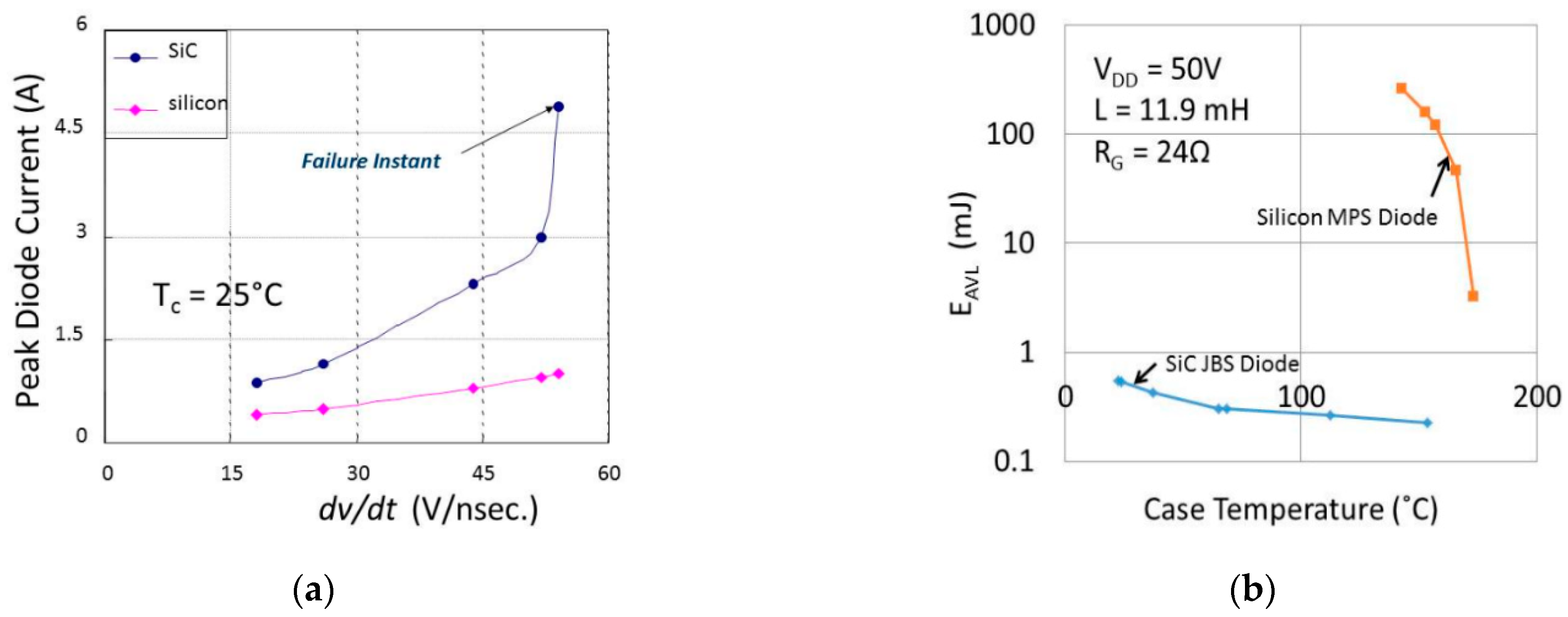
Figure 1b), results in local regions of elevated thermal dissipation or “hot spots” that cause loss of electrical functionality in SiC, even at moderately low
dv/
dt values (see
Figure 2a)
[25]. To date, there is no convincing explanation of this physical mechanism, although there is experimental indication showing a correlation between “hot spots” and defects. A fundamental requirement of semiconductor materials in such high-power applications is the ability to withstand localized Joule heating. It was shown that the worst-case Joule heating occurs when the semiconductor power switch is experiencing a simultaneous high-current and high-voltage condition, often referred to as an “avalanche state”
[26][27]. This situation typically occurs when the switch is short-circuited and/or absorbing the energy stored in a charged inductor. The measured avalanche energies of 600 V silicon and SiC power diodes are shown in
Figure 2b
[25].
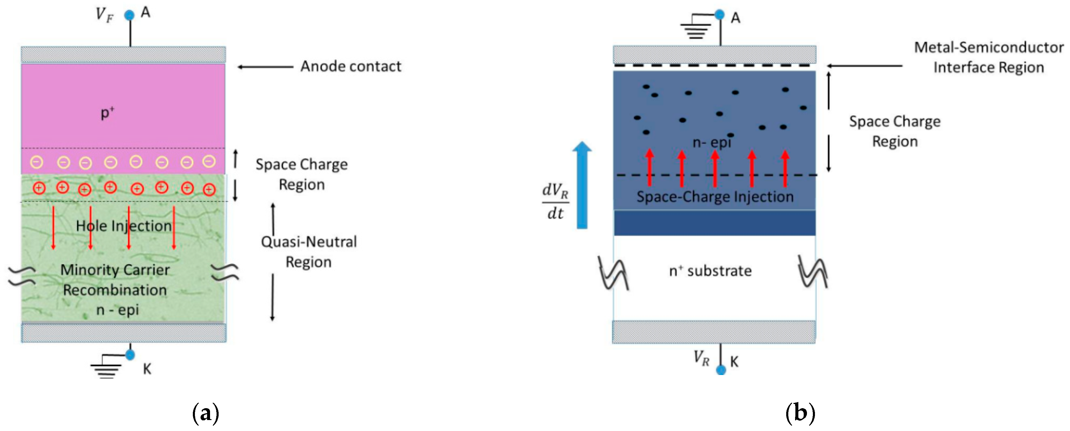
Figure 1. Potential mechanisms for defect excitation in a (
a) forward-biased bipolar semiconductor diode junction, and (
b) a unipolar Schottky barrier diode junction
[25].
 +1 credit