 +1 credit
| Version | Summary | Created by | Modification | Content Size | Created at | Operation |
|---|---|---|---|---|---|---|
| 1 | Chenguang He | + 1752 word(s) | 1752 | 2022-01-06 08:50:06 | | | |
| 2 | Jessie Wu | Meta information modification | 1752 | 2022-01-10 02:52:48 | | |
Video Upload Options
As a representative ultrawide bandgap (UWBG) semiconductor material, wurtzite aluminum nitride (AlN) material has many excellent properties such as high electron mobility (1100 cm2/Vs), high breakdown voltage (11.7 MV/cm), high piezoelectric coefficient, high thermal conductivity (320 W/m·K), high hardness (nine on the Mohs scale), high corrosion resistance, high chemical and thermal stability, as well as high bulk acoustic wave velocity (11,270 m/s).
1. Introduction
AlN crystal has three possible structures: hexagonal wurtzite structure, cubic zinc blende structure, and rock salt structure [1]. Among them, metastable-phase cubic zinc blende structure and rock salt structure only exist in some special growth conditions. In most cases, the hexagonal wurtzite structure is needed because its excellent chemical stability is helpful to obtain highly reliable devices. However, the high chemical stability makes it quite challenging to grow high-crystalline-quality bulk AlN crystals. Growing bulk crystals from the melt, which is performed for most other III–V semiconductors, is no longer applicable to AlN because ultrahigh temperature and pressure are needed. Nowadays, bulk AlN crystals are nearly exclusively obtained by using the physical vapor transport (PVT) method (sublimation and recondensation), which has achieved low TDDs of 102–105 cm−2 [2]. Nevertheless, it still cannot solve the typical problems such as small size (<60 mm), high impurity concentration (1018–1019 cm−3), poor ultraviolet transparency (α265–280 nm = 14–21 cm−1), and high cost (>9000 USD/2 inch) [3]. Only a few companies can supply bulk AlN in the world, and the production capacity is very low due to the very long growth time and very low yield. As an alternative, depositing thin AlN films on foreign substrates such as sapphire, silicon (Si), and silicon carbide (SiC) has become the prevailing method to obtain AlN crystals [4][5][6]. These pseudo-substrates are also called AlN templates. Among them, the most commonly used foreign substrate is sapphire, which is commercially available in various sizes (2–8 inches) and surface orientations (c, m, r, and a planes). Importantly, the crystalline quality of AlN/sapphire template is relatively good, and the cost of AlN/sapphire template has been reduced to 250 USD/2 inch. The deposition methods include metal organic chemical vapor deposition (MOCVD), molecular beam epitaxy (MBE), hydride vapor phase deposition (HVPE), physical vapor deposition (PVD), pulsed laser deposition (PLD), and atomic layer deposition (ALD).
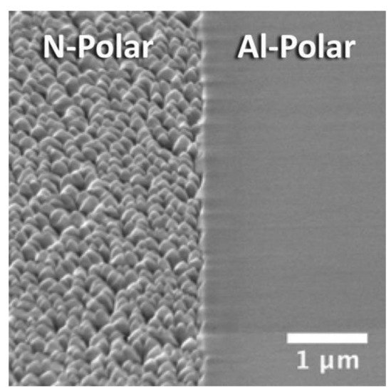
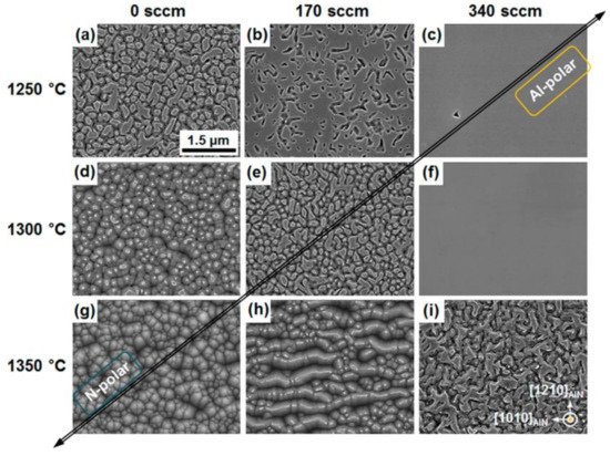
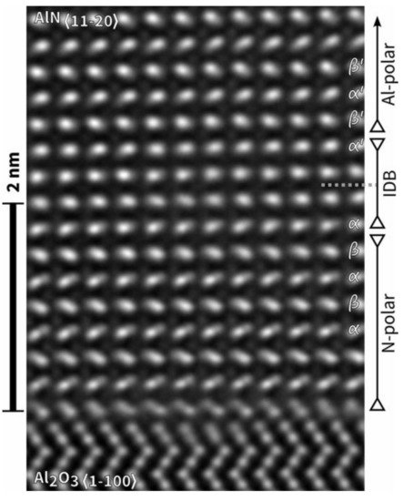
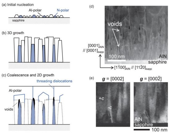
2. Polarity Control of AlN/Sapphire Template
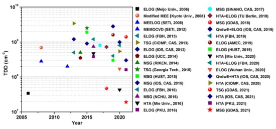
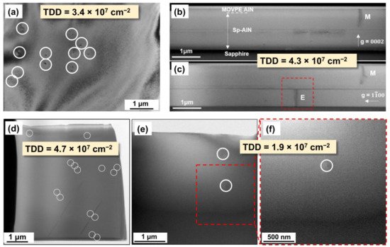
3. The TDD Compilation of AlN Films Grown by Different Techniques
References
- Li, D.; Jiang, K.; Sun, X.; Guo, C. AlGaN photonics: Recent advances in materials and ultraviolet devices. Adv. Opt. Photonics 2018, 10, 43–110.
- Yu, R.; Liu, G.; Wang, G.; Chen, C.; Xu, M.; Zhou, H.; Wang, T.; Yu, J.; Zhao, G.; Zhang, L. Ultrawide-bandgap semiconductor AlN crystals: Growth and applications. J. Mater. Chem. C 2021, 9, 1852–1873.
- Wang, Q.; Lei, D.; He, G.; Gong, J.; Huang, J.; Wu, J. Characterization of 60 mm AlN Single Crystal Wafers Grown by the Physical Vapor Transport Method. Phys. Status Solidi A 2019, 216, 1900118.
- He, C.; Zhao, W.; Wu, H.; Zhang, S.; Zhang, K.; He, L.; Liu, N.; Chen, Z.; Shen, B. High-quality AlN film grown on sputtered AlN/sapphire via growth-mode modification. Cryst. Growth Des. 2018, 18, 6816–6823.
- Shen, J.; Yang, X.; Liu, D.; Cai, Z.; Wei, L.; Xie, N.; Xu, F.; Tang, N.; Wang, X.; Ge, W. High quality AlN film grown on a nano-concave-circle patterned Si substrate with an AlN seed layer. Appl. Phys. Lett. 2020, 117, 22103.
- Zollner, C.J.; Almogbel, A.; Yao, Y.; SaifAddin, B.K.; Wu, F.; Iza, M.; DenBaars, S.P.; Speck, J.S.; Nakamura, S. Reduced dislocation density and residual tension in AlN grown on SiC by metalorganic chemical vapor deposition. Appl. Phys. Lett. 2019, 115, 161101.
- Ambacher, O.; Smart, J.; Shealy, J.; Weimann, N.; Chu, K.; Murphy, M.; Schaff, W.; Eastman, L.; Dimitrov, R.; Wittmer, L. Two-dimensional electron gases induced by spontaneous and piezoelectric polarization charges in N-and Ga-face AlGaN/GaN heterostructures. J. Appl. Phys. 1999, 85, 3222–3233.
- Guo, W.; Sun, H.; Torre, B.; Li, J.; Sheikhi, M.; Jiang, J.; Li, H.; Guo, S.; Li, K.H.; Lin, R. Lateral-polarity structure of AlGaN quantum wells: A promising approach to enhancing the ultraviolet luminescence. Adv. Funct. Mater. 2018, 28, 1802395.
- Ito, T.; Sakamoto, R.; Isono, T.; Yao, Y.; Ishikawa, Y.; Okada, N.; Tadatomo, K. Growth and Characterization of Nitrogen-Polar AlGaN/AlN Heterostructure for High-Electron-Mobility Transistor. Phys. Status Solidi. B 2020, 257, 1900589.
- Kirste, R.; Mita, S.; Hussey, L.; Hoffmann, M.P.; Guo, W.; Bryan, I.; Bryan, Z.; Tweedie, J.; Xie, J.; Gerhold, M. Polarity control and growth of lateral polarity structures in AlN. Appl. Phys. Lett. 2013, 102, 181913.
- Lemettinen, J.; Okumura, H.; Kim, I.; Rudzinski, M.; Grzonka, J.; Palacios, T.; Suihkonen, S. MOVPE growth of nitrogen-and aluminum-polar AlN on 4H-SiC. J. Cryst. Growth 2018, 487, 50–56.
- Eom, D.; Kim, J.; Lee, K.; Jeon, M.; Heo, C.; Pyeon, J.; Nam, O. AlN nanostructures fabricated on a vicinal sapphire (0001) substrate. Cryst. Growth Des. 2015, 15, 1242–1248.
- Akiyama, T.; Saito, Y.; Nakamura, K.; Ito, T. Nitridation of Al2O3 surfaces: Chemical and structural change triggered by oxygen desorption. Phys. Rev. Lett. 2013, 110, 26101.
- McCauley, J.W.; Patel, P.; Chen, M.; Gilde, G.; Strassburger, E.; Paliwal, B.; Ramesh, K.; Dandekar, D.P. AlON: A brief history of its emergence and evolution. J. Eur. Ceram. Soc. 2009, 29, 223–236.
- Sun, H.; Wu, F.; Park, Y.J.; Al Tahtamouni, T.; Li, K.-H.; Alfaraj, N.; Detchprohm, T.; Dupuis, R.D.; Li, X. Influence of TMAl preflow on AlN epitaxy on sapphire. Appl. Phys. Lett. 2017, 110, 192106.
- Wang, J.; Xu, F.; He, C.; Zhang, L.; Lu, L.; Wang, X.; Qin, Z.; Shen, B. High quality AlN epilayers grown on nitrided sapphire by metal organic chemical vapor deposition. Sci. Rep. 2017, 7, 42747.
- Miyagawa, R.; Yang, S.; Miyake, H.; Hiramatsu, K.; Kuwahara, T.; Mitsuhara, M.; Kuwano, N. Microstructure of AlN grown on a nucleation layer on a sapphire substrate. Appl. Phys. Express 2012, 5, 25501.
- Mohn, S.; Stolyarchuk, N.; Markurt, T.; Kirste, R.; Hoffmann, M.P.; Collazo, R.; Courville, A.; Di Felice, R.; Sitar, Z.; Vennéguès, P. Polarity control in group-III nitrides beyond pragmatism. Phys. Rev. Appl. 2016, 5, 54004.
- Funato, M.; Shibaoka, M.; Kawakami, Y. Heteroepitaxy mechanisms of AlN on nitridated c-and a-plane sapphire substrates. J. Appl. Phys. 2017, 121, 85304.
- Banal, R.G.; Funato, M.; Kawakami, Y. Initial nucleation of AlN grown directly on sapphire substrates by metal-organic vapor phase epitaxy. Appl. Phys. Lett. 2008, 92, 241905.
- Shatalov, M.; Sun, W.; Lunev, A.; Hu, X.; Dobrinsky, A.; Bilenko, Y.; Yang, J.; Shur, M.; Gaska, R.; Moe, C. AlGaN deep-ultraviolet light-emitting diodes with external quantum efficiency above 10%. Appl. Phys. Express 2012, 5, 82101.
- He, C.; Wu, H.; Jia, C.; Zhang, K.; He, L.; Wang, Q.; Li, J.; Liu, N.; Zhang, S.; Zhao, W. Low-Defect-Density Aluminum Nitride (AlN) Thin Films Realized by Zigzag Macrostep-Induced Dislocation Redirection. Cryst. Growth Des. 2021, 21, 3394–3400.
- Hirayama, H.; Maeda, N.; Fujikawa, S.; Toyoda, S.; Kamata, N. Recent progress and future prospects of AlGaN-based high-efficiency deep-ultraviolet light-emitting diodes. Jpn. J. Appl. Phys. 2014, 53, 100209.
- Yan, J.; Wang, J.; Zhang, Y.; Cong, P.; Sun, L.; Tian, Y.; Zhao, C.; Li, J. AlGaN-based deep-ultraviolet light-emitting diodes grown on high-quality AlN template using MOVPE. J. Cryst. Growth 2015, 414, 254–257.
- Imura, M.; Nakano, K.; Kitano, T.; Fujimoto, N.; Narita, G.; Okada, N.; Balakrishnan, K.; Iwaya, M.; Kamiyama, S.; Amano, H. Microstructure of epitaxial lateral overgrown AlN on trench-patterned AlN template by high-temperature metal-organic vapor phase epitaxy. Appl. Phys. Lett. 2006, 89, 221901.
- Long, H.; Dai, J.; Zhang, Y.; Wang, S.; Tan, B.; Zhang, S.; Xu, L.; Shan, M.; Feng, Z.C.; Kuo, H.-c. High quality 10.6 μ m AlN grown on pyramidal patterned sapphire substrate by MOCVD. Appl. Phys. Lett. 2019, 114, 42101.
- Zeimer, U.; Kueller, V.; Knauer, A.; Mogilatenko, A.; Weyers, M.; Kneissl, M. High quality AlGaN grown on ELO AlN/sapphire templates. J. Cryst. Growth 2013, 377, 32–36.
- Dong, P.; Yan, J.; Wang, J.; Zhang, Y.; Geng, C.; Wei, T.; Cong, P.; Zhang, Y.; Zeng, J.; Tian, Y.; et al. 282-nm AlGaN-based deep ultraviolet light-emitting diodes with improved performance on nano-patterned sapphire substrates. Appl. Phys. Lett. 2013, 102, 241113.
- Conroy, M.; Zubialevich, V.Z.; Li, H.; Petkov, N.; Holmes, J.D.; Parbrook, P.J. Epitaxial lateral overgrowth of AlN on self-assembled patterned nanorods. J. Mater. Chem. C 2015, 3, 431–437.
- Zhang, L.; Xu, F.; Wang, J.; He, C.; Guo, W.; Wang, M.; Sheng, B.; Lu, L.; Qin, Z.; Wang, X. High-quality AlN epitaxy on nano-patterned sapphire substrates prepared by nano-imprint lithography. Sci. Rep. 2016, 6, 35934.
- Miyake, H.; Nishio, G.; Suzuki, S.; Hiramatsu, K.; Fukuyama, H.; Kaur, J.; Kuwano, N. Annealing of an AlN buffer layer in N2–CO for growth of a high-quality AlN film on sapphire. Appl. Phys. Express 2016, 9, 25501.
- Ben, J.; Shi, Z.; Zang, H.; Sun, X.; Liu, X.; Lü, W.; Li, D. The formation mechanism of voids in physical vapor deposited AlN epilayer during high temperature annealing. Appl. Phys. Lett. 2020, 116, 251601.
- Wang, D.; Uesugi, K.; Xiao, S.; Norimatsu, K.; Miyake, H. Low dislocation density AlN on sapphire prepared by double sputtering and annealing. Appl. Phys. Express 2020, 13, 95501.
- Susilo, N.; Hagedorn, S.; Jaeger, D.; Miyake, H.; Zeimer, U.; Reich, C.; Neuschulz, B.; Sulmoni, L.; Guttmann, M.; Mehnke, F.; et al. AlGaN-based deep UV LEDs grown on sputtered and high temperature annealed AlN/sapphire. Appl. Phys. Lett. 2018, 112, 41110.
- Wang, J.; Xu, F.; Liu, B.; Lang, J.; Zhang, N.; Kang, X.; Qin, Z.; Yang, X.; Wang, X.; Ge, W.; et al. Control of dislocations in heteroepitaxial AlN films by extrinsic supersaturated vacancies introduced through thermal desorption of heteroatoms. Appl. Phys. Lett. 2021, 118, 162103.
- Liu, Z.; Guo, Y.; Yan, J.; Zeng, Y.; Wang, J.; Li, J. Polarity tuning of crystalline AlN films utilizing trace oxygen involved sputtering and post-high-temperature annealing. Appl. Phys. Express 2021, 14, 85501.
- Chang, H.; Chen, Z.; Li, W.; Yan, J.; Hou, R.; Yang, S.; Liu, Z.; Yuan, G.; Wang, J.; Li, J. Graphene-assisted quasi-van der Waals epitaxy of AlN film for ultraviolet light emitting diodes on nano-patterned sapphire substrate. Appl. Phys. Lett. 2019, 114, 91107.
- Chang, H.; Liu, B.; Liang, D.; Gao, Y.; Yan, J.; Liu, Z.; Liu, Z.; Wang, J.; Li, J.; Gao, P. Graphene-induced crystal-healing of AlN film by thermal annealing for deep ultraviolet light-emitting diodes. Appl. Phys. Lett. 2020, 117, 181103.
- Jain, R.; Sun, W.; Yang, J.; Shatalov, M.; Hu, X.; Sattu, A.; Lunev, A.; Deng, J.; Shturm, I.; Bilenko, Y. Migration enhanced lateral epitaxial overgrowth of AlN and AlGaN for high reliability deep ultraviolet light emitting diodes. Appl. Phys. Lett. 2008, 93, 51113.
- Sun, X.; Li, D.; Chen, Y.; Song, H.; Jiang, H.; Li, Z.; Miao, G.; Zhang, Z. In situ observation of two-step growth of AlN on sapphire using high-temperature metal–organic chemical vapour deposition. CrystEngComm 2013, 15, 6066–6073.
- Li, X.H.; Wang, S.; Xie, H.; Wei, Y.O.; Kao, T.T.; Satter, M.M.; Shen, S.C.; Douglas Yoder, P.; Detchprohm, T.; Dupuis, R.D. Growth of high-quality AlN layers on sapphire substrates at relatively low temperatures by metalorganic chemical vapor deposition. Phys. Status Solidi B 2015, 252, 1089–1095.
- Chen, S.; Li, Y.; Ding, Y.; Li, S.; Zhang, M.; Wu, Z.; Fang, Y.; Dai, J.; Chen, C. Defect reduction in AlN epilayers grown by MOCVD via intermediate-temperature interlayers. J. Electron. Mater. 2015, 44, 217–221.
- Hagedorn, S.; Knauer, A.; Mogilatenko, A.; Richter, E.; Weyers, M. AlN growth on nano-patterned sapphire: A route for cost efficient pseudo substrates for deep UV LEDs. Phys. Status Solidi A 2016, 213, 3178–3185.
- Wang, T.Y.; Liang, J.H.; Fu, G.W.; Wuu, D.S. Defect annihilation mechanism of AlN buffer structures with alternating high and low V/III ratios grown by MOCVD. CrystEngComm 2016, 18, 9152–9159.
- Su, X.; Zhang, J.; Huang, J.; Zhang, J.; Wang, J.; Xu, K. Defect structure of high temperature hydride vapor phase epitaxy-grown epitaxial (0001) AlN/sapphire using growth mode modification process. J. Cryst. Growth 2017, 467, 82–87.
- Hagedorn, S.; Walde, S.; Mogilatenko, A.; Weyers, M.; Cancellara, L.; Albrecht, M.; Jaeger, D. Stabilization of sputtered AlN/sapphire templates during high temperature annealing. J. Cryst. Growth 2019, 512, 142–146.
- Chen, Z.; Hoo, J.; Chen, Y.; Wang, V.; Guo, S. Study of AlN based materials grown on nano-patterned sapphire substrates for deep ultraviolet LED applications. Jpn. J. Appl. Phys. 2019, 58, SC1007.
- Ruschel, J.; Glaab, J.; Susilo, N.; Hagedorn, S.; Walde, S.; Ziffer, E.; Cho, H.K.; Ploch, N.L.; Wernicke, T.; Weyers, M. Reliability of UVC LEDs fabricated on AlN/sapphire templates with different threading dislocation densities. Appl. Phys. Lett. 2020, 117, 241104.
- Tang, B.; Hu, H.; Wan, H.; Zhao, J.; Gong, L.; Lei, Y.; Zhao, Q.; Zhou, S. Growth of high-quality AlN films on sapphire substrate by introducing voids through growth-mode modification. Appl. Surf. Sci. 2020, 518, 146218.
- Moram, M.; Vickers, M. X-ray diffraction of III-nitrides. Rep. Prog. Phys. 2009, 72, 36502.
- Koleske, D.; Figiel, J.; Alliman, D.; Gunning, B.; Kempisty, J.; Creighton, J.; Mishima, A.; Ikenaga, K. Metalorganic vapor phase epitaxy of AlN on sapphire with low etch pit density. Appl. Phys. Lett. 2017, 110, 232102.

