As a representative ultrawide bandgap (UWBG) semiconductor material, wurtzite aluminum nitride (AlN) material has many excellent properties such as high electron mobility (1100 cm2/Vs), high breakdown voltage (11.7 MV/cm), high piezoelectric coefficient, high thermal conductivity (320 W/m·K), high hardness (nine on the Mohs scale), high corrosion resistance, high chemical and thermal stability, as well as high bulk acoustic wave velocity (11,270 m/s).
1. Introduction
AlN crystal has three possible structures: hexagonal wurtzite structure, cubic zinc blende structure, and rock salt structure [1][15]. Among them, metastable-phase cubic zinc blende structure and rock salt structure only exist in some special growth conditions. In most cases, the hexagonal wurtzite structure is needed because its excellent chemical stability is helpful to obtain highly reliable devices. However, the high chemical stability makes it quite challenging to grow high-crystalline-quality bulk AlN crystals. Growing bulk crystals from the melt, which is performed for most other III–V semiconductors, is no longer applicable to AlN because ultrahigh temperature and pressure are needed. Nowadays, bulk AlN crystals are nearly exclusively obtained by using the physical vapor transport (PVT) method (sublimation and recondensation), which has achieved low TDDs of 102–105 cm−2 [2]. Nevertheless, it still cannot solve the typical problems such as small size (<60 mm), high impurity concentration (1018–1019 cm−3), poor ultraviolet transparency (α265–280 nm = 14–21 cm−1), and high cost (>9000 USD/2 inch) [3][16]. Only a few companies can supply bulk AlN in the world, and the production capacity is very low due to the very long growth time and very low yield. As an alternative, depositing thin AlN films on foreign substrates such as sapphire, silicon (Si), and silicon carbide (SiC) has become the prevailing method to obtain AlN crystals [4][5][6][17,18,19]. These pseudo-substrates are also called AlN templates. Among them, the most commonly used foreign substrate is sapphire, which is commercially available in various sizes (2–8 inches) and surface orientations (c, m, r, and a planes). Importantly, the crystalline quality of AlN/sapphire template is relatively good, and the cost of AlN/sapphire template has been reduced to 250 USD/2 inch. The deposition methods include metal organic chemical vapor deposition (MOCVD), molecular beam epitaxy (MBE), hydride vapor phase deposition (HVPE), physical vapor deposition (PVD), pulsed laser deposition (PLD), and atomic layer deposition (ALD).
2. Polarity Control of AlN/Sapphire Template
The polarity control is very important for AlN-based devices, because polarity greatly affects the electronic and optoelectronic properties by changing the pyroelectric and piezoelectric fields
[7][20]. The polarities of AlN include Al-polarity (+
c-polarity) and N-polarity (−
c-polarity). Except for some special applications such as lateral polarity structure (LPS) and N-polar high electron mobility transistors (HEMTs)
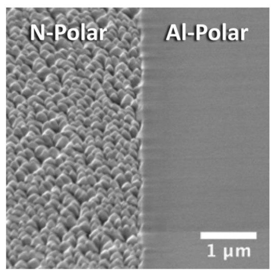
[8][9][21,22], N-polar AlN is not desired because of its poor crystalline quality, surface morphology, and chemical stability. Ronny Kirste et al. demonstrated the surface of N-polar AlN was dominated by a typical columnar morphology, with an average width of ~500 nm and a height difference of ~100 nm
[10][23], as shown in
Figure 1. The rough surface morphology originated from the presence of Al-polar inversion domains (IDs), which had a faster growth rate along the [0001] direction. Other studies have also confirmed that N-polar AlN usually coexists with Al-polar AlN IDs, meaning that AlN film grown on sapphire substrate generally exists in two forms: Al-polar AlN and mixed-polar AlN. To realize large-area pure N-polar AlN, C-face SiC substrate may be the better choice
[11][24]. The mixed-polar AlN can be confirmed by the KOH solution etching because N-polar AlN has an obvious faster etching rate compared with Al-polar AlN.
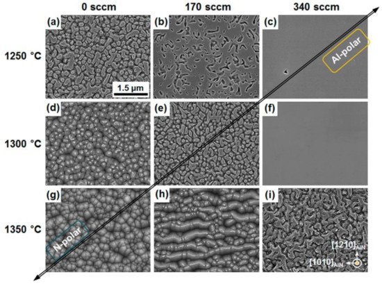
Figure 2 displays some etched surfaces of AlN epilayers grown in different conditions
[12][25]. The etched parts are N-polar AlN, and the residual parts are Al-polar AlN.
Figure 1. Morphology difference between N-polar and Al-polar AlN on the same wafer. Reprinted from
[10][23], with the permission of AIP Publishing.
Figure 2. (
a–
i) Plan-view scanning electron microscope (SEM) images of KOH-etched AlN/sapphire templates, which were grown on different conditions (Temperatures = 1250, 1300, and 1350 °C; TMAl flows = 0, 170, and 340 sccm). Reprinted with permission from
[12][25]. Copyright {2015} American Chemical Society.
Compared with other nitride semiconductors, the polarity control of AlN film grown on sapphire substrate is much more difficult. It is attributed to the formation of unevenly distributed aluminum-oxynitride (Al
xO
yN
z) phases near the AlN/sapphire interface, which is responsible for the appearance of mixed-polar AlN. Al
xO
yN
z phases can exist with various stoichiometric ratios, depending on the competition result of Al, O, and N atoms
[13][26]. Since the 1970s, various Al
xO
yN
z phases have been established, including 20
H (Al
10O
3N
8), 27
R (Al
9O
3N
7), 16
H (Al
8O
3N
6), 21
R (Al
7O
3N
5), 12
H (Al
6O
3N
4), and many other phases
[14][27]. These O atoms may come from sapphire substrate, precursors and chambers, so they are hard to completely eliminate. To suppress the undesired N-polar AlN/mixed-polar AlN, we need to find out the key factors affecting polarity control in the presence of O atoms.
H. D. Sun et al. found that proper TMAl pretreatment promoted the formation of Al-polar AlN, because carbon (C) impurities dissociated from TMAl precursor could attract surrounding O impurities and suppress the formation of Al
xO
yN
z phases
[15][28]. Cross-sectional energy-loss spectroscopy spectrum (EELS) demonstrated that the distributions of C and O atoms above the AlN/sapphire interface are highly consistent. J. M. Wang et al. found that 7 s NH
3 preflow (nitridation) could also maintain Al-polar AlN, and the
c-axis orientation was very good
[16][29]. However, a longer-time NH
3 preflow resulted in the formation of mixed-polar AlN. Obviously, the pretreatment process before the deposition of AlN film is very important. Additionally, it was found that high initial growth temperature facilitates the formation of N-polar AlN. Reina Miyagawa et al. revealed that a certain chemical reaction occurred during the high-temperature growth process, causing the exchange of O atoms in sapphire substrate and N atoms in AlN epilayer in some areas
[17][30]. As a result, Al-polar and N-polar AlN simultaneously appeared and coexisted in the subsequent growth process, because the large N-polar AlN grains at high growth temperature were hard to bury.
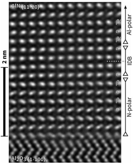
In some special cases, the transition from pure N-polar or mixed-polar AlN to pure Al-polar AlN may occur. Stefan Mohn et al. demonstrated that pure N-polar AlN could be entirely converted into Al-polar AlN within 3 nm, with the help of a flat rhombohedral Al
xO
yN
z layer
[18][31]. Scanning transmission electron microscope (STEM) and high-resolution transmission electron microscopy (HRTEM) images revealed that the conversion had been completed during the nitridation process before growth, as shown in
Figure 3. However, excessive annealing may destroy the Al
xO
yN
z structure, leading to incomplete coverage of the Al
xO
yN
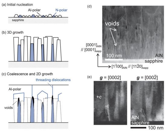
z layer, especially when the annealing temperature is very high. In this situation, the undesirable mixed-polar AlN is formed due to the incomplete conversion of N-polar AlN to Al-polar AlN. Mitsuru Funato et al. reported that N-polar AlN domains in mixed-polar AlN could be buried by their surrounding Al-polar AlN, as shown in
Figure 4. This phenomenon occurred when the nitridation of sapphire substrate initiated at a low temperature of 100 °C
[19][32]. The elimination of N-polar AlN domains benefited from the small size of inversion domains and the faster growth rate of Al-polar AlN
[12][25]. Based on the above analysis, we can see that the realization of pure Al-polar AlN has three approaches: suppressing the local formation of Al
xO
yN
z phases in the initial stage, converting N-polar to Al-polar AlN by the complete coverage of ultrathin Al
xO
yN
z layer, and burying N-polar AlN by the lateral overgrowth of Al-polar AlN.
Figure 3. Cross-sectional HRTEM image of AlN/sapphire template. The polarity of AlN epilayer evolved from N-polar to Al-polar within 3 nm above the AlN/sapphire interface. Reprinted from
[18][31] under the terms of the Creative Commons Attribution 3.0 License.
Figure 4. Schematic diagrams of the lateral burying process of N-polar AlN by Al-polar AlN: (
a) the initial nucleation stage; (
b) 3D growth stage; (
c) coalescence and 2D growth stage; (
d) cross-sectional TEM image of the lateral burying process of N-polar AlN by Al-polar AlN. Lots of voids formed above the N-polar AlN after the entire burying of N-polar AlN; (
e) cross-sectional TEM dark field (DF) images taken at the same position using two-beam conditions. Lots of columnar structures with a width of tens of nanometers can be observed, indicating the co-existence of Al-polar AlN and N-polar AlN. Reprinted from
[19][32], with the permission of AIP Publishing.
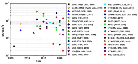
34. The TDD Compilation of AlN Films Grown by Different Techniques
Figure 5 summarizes the reported TDD values (2005–2021) of AlN films grown by different techniques. The laboratory level of TDD can be decreased to <5 × 107 cm−2 by using ELOG, HTA, and MSG growth techniques, and the industrialization level of TDD is decreased to 108–109 cm−2.
Figure 5. Selected AlN/sapphire TDD by year of publication
[4][20][21][22][23][24][25][26][27][28][29][30][31][32][33][34][35][36][37][38][39][40][41][42][43][44][45][46][47][48][49][17,36,40,42,43,46,53,56,58,59,60,62,69,73,74,76,79,81,94,98,99,100,101,102,103,104,105,106,107,108,109]. The ultralow TDD value of 3.4 × 10
7 cm
−2 has been achieved by ELOG growth technique in 2006. Since 2018, MSG and HTA growth techniques have also achieved ultralow TDD values below 5 × 10
7 cm
−2.
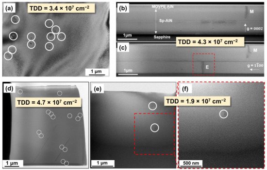
It is noted that there has been no unified standard for the evaluation of TDD. X-ray rocking curve (XRC) scan is the most common method to evaluate TDD. However, X-ray has a large penetration depth in AlN material, meaning that the measurement result containing the information of the whole AlN epilayer rather than that of the top AlN epilayer
[50][110]. Thus, the TDD of the top AlN epilayer extracted from XRC scan is usually overestimated, especially when the TDD is low. Cross-sectional TEM and plan-view TEM results can give the TDD of the top AlN layer, as shown in
Figure 6. Nevertheless, they have certain degrees of randomness, since the measurement area is usually <50 μm
2 [4][25][33][17,53,74]. Plan-view cathodoluminescence (CL) spectroscopy, which is frequently used to count the TDD of GaN epilayer, is no longer applicable to AlN because of the poor conductivity of AlN and the weak responsivity of the detector at ~200 nm. The TDD evaluated by etch pit density is also inaccurate when the AlN surface is under etched or over etched
[51][111]. Additionally, even if the measurement method is the same, different equipment may obtain different results. Therefore, strictly speaking, the TDD results from different groups or evaluated by different methods should not be directly compared. Here, we list some representative TDD values to see the general development trend.
Figure 6. (
a) Plan-view TEM image of ELOG-AlN grown by Meijo University. Reprinted from J. Cryst. Growth, 298, Masataka Imura et al., “Epitaxial lateral overgrowth of AlN on trench-patterned AlN layers”, 257–260, Copyright (2007), with permission from Elsevier. (
b,
c) Cross-sectional TEM images of HTA-AlN grown by Mie University. Reprinted from
[33][74]. Copyright (2020) The Japan Society of Applied Physics. (
d) Plan-view TEM image of 5.6 μm-thick MSG-AlN grown by Guangdong Academy of Sciences (GDAS). Reprinted with permission from
[4][17]. Copyright {2018} American Chemical Society. (
e,
f) Plan-view TEM images of 11 μm-thick MSG-AlN grown by GDAS.