1. Introduction
Globe environment pollution and energy crisis have become the major issues accompanied with the economic growth owing to the excessive consumption of fossil resources. Searching for alternative renewable energy is one of the most significant technologies to solve the urgent problems
[1][2]. Solar energy has become an ideal energy resource due to its inexhaustible, widespread, and environmentally friendly characteristics, which can be effectively exploited and converted into electricity
[3][4][5][6]. Organic solar cells (OSCs) as one of the third-generation photovoltaics have achieved rapid development currently, which exhibit great advantages for their low cost, light weight, simple manufacture, and large-area fabrication
[7][8][9]. In recent years, the performance of the OSCs has been dramatically improved with the emergence of the non-fullerene acceptor and the relevant donor materials
[7][10][11][12][13][14][15], which leads to the tremendous breakthroughs in power conversion efficiencies (PCE) of the OSCs. According to the theoretical calculations, it is reported the highest efficiency of the single-junction non-fullerene acceptor-based OSCs (NFA-OSCs) is expected to exceed 20%
[16][17][18][19][20][21]. However, the NFA-OSCs are still confronted with several challenges compared with other high-efficient photovoltaics. Particularly, the relatively low device efficiency and long-term instability of the OSCs limit their industrial production and commercialization
[22][23][24]. The serious electron-hole recombination, low carrier mobility of the active layers, and insufficient sunlight absorption are taking the main responsibility for the limited PCE of the OSCs. Besides, it is well acknowledged that the most commonly used hole transport layer (HTL) material, Poly(3,4-ethylenedioxythiophene):poly(styrenesulfonate) (PEDOT:PSS) exhibits hygroscopicity characteristic, which can easily corrode the indium tin oxide (ITO) electrode material, decreasing the efficiency and stability of the devices
[25][26][27][28][29].
Lots of strategies have been applied to improve the efficiency and stability of the OSCs
[4][11][12][18]. For example, the introduction of metal nanostructures into the OSCs can increase the light absorption capacity of the active layer with a plasma enhancement effect
[30][31][32], increasing the PCE of photovoltaic devices. Owing to the quantum size effect, the addition of quantum dots into the active layer of the OSCs can harvest more sunlight from the wider band of the solar spectrum for enhancing the efficiency of the devices
[33][34][35][36]. Nanowires with conductive properties can replace ITO as electrode materials of the OSCs with superior stability and competitive photovoltaic performances
[37][38][39][40][41].
Among the variety of the nanomaterials applied in the OSCs, 2D layered materials can be considered as promising candidates for the application in different positions of the OSCs due to their excellent optoelectronic characteristics, tunable energy band structure, and relatively stable physical and chemical properties
[42][43][44][45][46][47][48]. Most of the 2D nanomaterials have a typical layered structures with solution-processability
[6][25][26][38][44][45]. In
Table 1, we list a few typical 2D materials and their key physical parameters. The 2D materials, such as WSe
2, BP, etc. with tunable bandgaps exhibit carrier mobilities several orders of magnitude higher than those of the organic semiconductors in OSCs.
Table 1. The physical parameters of a few novel 2D materials applied in OSCs.
| Materials |
Bandgap (eV) |
Carrier Mobility (cm2 V−1 s−1) |
Ref. |
| WSe2 |
1.2–1.7 |
500 |
[49] |
| MoSe2 |
1.5 |
50 |
[50] |
| Bi2O2S |
1.27 |
16,000–26,000 |
[51] |
| α-In2Se3 |
1.5–2.8 |
2.5 |
[52] |
| BP |
0.3–2.0 |
1000 |
[53] |
| Ti3C2Tx |
0–3.4 |
0.70 |
[54] |
| Graphene |
0 |
1000 |
[55] |
| MoS2 |
1.2–1.8 |
10–200 |
[56] |
The incorporation of suitable 2D materials into the OSCs, not only can enhance the light absorption and scattering in the devices, but also improve the charge transport and suppress the carrier recombination, leading to an enhancement of PCE with the increased fill factor (FF) and short-circuit current density (Jsc) of the OSCs. Besides, appropriate 2D materials can replace the unstable PEDOT:PSS layer or evaporated electrodes for improving the stability and simplifying the fabrication process of the OSCs.
2. The Application of 2D Materials in the Active Layer
To achieve high-performance OSCs, 2D materials involved in the active layer of the photovoltaic devices as the third components have aroused widespread concerns. Graphene has attracted tremendous attention since being synthesized in 2004
[57], which possess excellent carrier mobility. And its derivative graphene oxide (GO) by solution-processable exfoliation of graphene has also been extensively studied in the field of organic optoelectronic devices due to the high carrier mobility, great conductivity, and solution dispersibility at the presence of oxygen functional groups
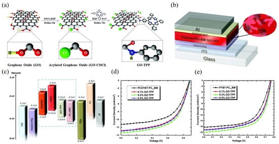
[58][59][60][61][62]. In 2015, Stylianakis et al. synthesized the graphene-based porphyrin molecule (GO-TPP) as an additive in the active layer of OSCs
[63]. Simply by covalent interaction between the GO and 5-(4-aminophenyl)-10,15,20-triphenyl) porphyrin (TPP-NH
2) as shown in
Figure 1a, the TPP-NH
2 porphyrin presents π aromatic framework with excellent stability and light-harvesting capacity. As presented in
Figure 1b, the OSCs based on PCDTBT:PC
71BM and PTB7:PC
71BM were fabricated, respectively, which exhibited the device structure of ITO/PEDOT:PSS/Active layer + GO-TTP/TiO
x/Ca/Al. The incorporation of GO-TPP enabled to optimize the band structure of the device with cascaded energy levels between the donor and acceptor as shown in
Figure 1c. Moreover, it provided continuous penetration paths between the donor and acceptor interfaces, which led to the suppression of exciton recombination and the promotion of charge transport. As shown in
Figure 1d,e. The best PCEs of 7.13% and 8.81% in the PCDTBT:PC
71BM and PTB7:PC
71BM-based OSCs were achieved, respectively by adding the optimum concentration of 0.3% GO-TPP.
Figure 1. Schematic representation of (
a) the chemical synthesis of GO-TPP and (
b) the photovoltaic device; (
c) Energy level diagram of the photovoltaic device; The J-V curves of the OSCs based on (
d) PCDTBT:PC
71BM and (
e) PTB7:PC
71BM with different concentrations of GO-TPP. Reprinted with permission from
[63]. Copyright 2015 The Royal Society of Chemistry.
Among the variety of 2D nanomaterials, besides graphene and its derivatives, transition metal dichalcogenides (TMDs) are the most widely studied materials, which are formed by the transition metal atom such as W, Mo, Pd, Pt et al. sandwiched among the chalcogenide atoms such as Se, S, Te. TMDs like WSe2 that have been studied in the early, exhibits high mobility around 500 cm2 V−1 s−1 and 104 on/off ratios at 60 k. MoS2 is also a popular TMD material with high mobility of 200 cm2 V−1 s−1 at room temperature. The bandgap of 2D WS2 is more than 2 eV, while the 2D MoS2 is approximately 1.2–1.9 eV. The TMDs with different thicknesses related to the nanoscale domain sizes of the active layer have distinctly different effects on the performance of the OSCs.
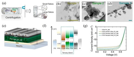
In 2017, Kymakis et al. incorporated WSe
2 flakes into the active layer of PTB7:PC
71BM-based OSCs
[64]. As shown in
Figure 2a. They exploited the sedimentation-based separation to sort the WSe
2 flakes by ultracentrifugation with different centrifugal speeds, which obtained different sizes of WSe
2 with ~70, ~240, and ~720 nm
2, respectively (see
Figure 2b–d). The structure of the device based on PTB7:PC
71BM:WSe
2 was displayed in
Figure 2e. The bandgap of WSe
2 could be tuned with the thickness variation from 0.8 eV in the bulk to 1.3 eV in the single layer, which provides matchable energy levels to improve the carrier mobility, exciton dissociation, and charge extraction (seen in
Figure 2f). It is demonstrated that the incorporation of WSe
2 flakes with a similar size to the domain of the active layer led to the best PCE s for the OSCs due to the optimized percolation pathways for charge transport. Therefore, the champion devices based on PTB7:PC
71BM with the incorporation of ~240 nm
2 WSe
2 achieved the PCE of 9.45%, enhancing by 16.67% compared with the control devices, as shown in
Figure 2g. This research quantitatively illustrated the relationship between the 2D nanomaterial and domain sizes of the active layer, indicating the effective strategy to control the area and thickness of the 2D materials for improving the photovoltaic performance of the OSCs and other photovoltaics.
Figure 2. Schematic representation of (
a) the fabrication of WSe
2 flakes by ultracentrifugation depended on SBS method and the separation of different sizes of WSe
2 flakes; TEM images of WSe
2 flakes with different area values of (
b) ~70, (
c) ~240 and (
d) ~720nm
2, respectively; (
e) The device structure of ternary OSCs with incorporation of WSe
2 flakes in the active layer; (
f) Schematic energy levels and (
g) J-V curves of the OSCs based on PTB7:PC
71BM. Reprinted with permission form
[64]. Copyright 2017 American Chemical Society.
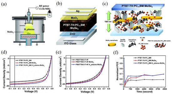
To further enrich the application of 2D TMDs materials in the OSCs, it is of necessity to exploit new methods for the functionalization of TMDs materials. In 2019, Wei et al. adopted the hydrogen plasma treatment to modify the properties of MoSe
2 as shown in
Figure 3a
[65]. Hydrogenated MoSe
2 nanosheets will form the H-Se-Mo bonds, which can lead to the electron transfer from the hydrogen atoms to the selenium atoms, enhancing the repulsive forces among selenium atoms and increasing the quantities of the produced photoelectrons. Hydrogenated MoSe
2 was subsequently applied in the OSCs based on PTB7-Th:PC
71BM in the active layer as displayed in
Figure 3b. The incorporation of hydrogenated MoSe
2 in the ternary blend optimized the morphology of the active layer and served as additional conducting bridges for the charge transfer, improving the carrier mobility in the devices (seen in
Figure 3c). As shown in
Figure 3d,e, the champion devices based on PTB7-Th:PC
71BM and PBDTTBOIT-4F reached 10.44% and 8.13%, respectively by incorporating the hydrogen plasma-treated MoSe
2 nanosheets in the active layer. Moreover, hydrogenated TMDs show great stability owing to the shorter bonding distance between the chalcogen atoms and hydrogen atoms than those between the chalcogen atoms and other atoms from density functional theory calculations. Thus, after thermal treatment at 100 °C for 1 h, the devices with the hydrogenated MoSe
2 maintained 70% of the original PCE compared with the reference devices with 60%, as exhibited in
Figure 3f.
Figure 3. (
a) Schematic representation of the H
2 plasma treatment; (
b) The device structure of inverted OSCs based on PTB7-Th:PC
71BM with MoSe
2; (
c) Schematic diagram of the interplay of MoSe
2 with PTB7-TH and PC
71BM; J-V characteristics of (
d) PTB7-Th:PC
71BM and (
e) PBDTTBO:IT-4F devices without MoSe
2 and introducing MoSe
2 with and without hydrogen plasma treatment; (
f) Stability of PCE values of devices based on PTB7-TH:PC
71BM without MoSe
2 and adding MoSe
2 with and without hydrogen plasma treatment at 100 °C. Reprinted with permission form
[65]. Copyright 2019 The Royal Society of Chemistry.
2D Black phosphorus (BP) is another novel layered semiconductor with an allotrope of phosphorus, which has extraordinarily high charge mobilities of about ~1000 cm
2 V
−1 s
−1 [45][55][56]. The bandgap of BP is adjustable from 0.3 to 1.8, and 2.1 eV, corresponding to the bulk, bilayers, and monolayer, respectively, which enables BP to match well with the bandgap of the donor and acceptor in the OSCs.
In 2019, Chen et al. studied the application of the embedded BP nanoflakes in the active layer of OSCs
[66]. They used the liquid-phase exfoliation method to fabricate BP nanoflakes with the size of 46 nm and re-dispersed them in chlorobenzene. The incorporation of BP nanoflakes can form the π-π stacking ordering and optimize the phase purity of the active layer, contributing to the improved charge mobilities and suppressed charge recombination. As a result, the PCE of 12.2% can be obtained for the OSCs based on PTB7-Th:IEICO-4F with the Jsc of 23.94 mA cm
−2, Voc of 0.72 V, and FF of 0.73. Besides, the thermal stability of the device with BP nanoflakes was investigated by thermal treatment at 150 °C, which remains 73% of the original PCE compared with the reference device of 60%.
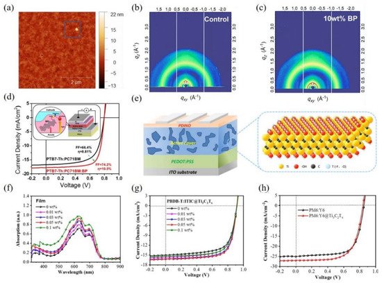
However, the traditional exfoliation method for the fabrication of BP may limit the application due to the poor dispersibility of BP clusters in organic solvents. Liu et al. exhibited a one-step solvothermal method to produce BP from the cheap and available white phosphorus and also incorporated them into the active layer of the OSCs
[67]. Due to the noncovalent interactions between PTB7-Th and BP, the uniform and continuous active layer can be observed in the AFM image as shown in
Figure 4a, additionally, the 2D GIWAXS patterns (see
Figure 4b,c) displayed similar diffraction patterns in the active layer with or w/o BP incorporation, which illustrated the BP hardly affected the crystallization of donor and acceptor and the phase separation of the active layer. As indicated in
Figure 4d, the PCE of 10.5% was realized in the device based on PTB7-Th:PC
71BM incorporating with 10 wt% BP in the active layer, resulting from the improvement of the carrier mobility and charge collection.
Carrier mobility is one of the key factors to determine the device performance A few 2D materials like bismuth oxychalcogenides (Bi
2O
2X) have a large surface area with excellent carrier mobility and high electron affinity, which can be applied in the photovoltaics
[68][69]. Besides, the Bi
2O
2X, such as Bi
2O
2S, Bi
2O
2Se and Bi
2O
2Te have suitable bandgaps about 1.27 eV, 0.8 eV and 0.11 eV, respectively. In 2019, Huang et al. reported the 2D Bi
2O
2S as a potential candidate for the performance improvement of the OSCs
[70]. The Bi
2O
2S nanomaterial synthesized by the hydrothermal method was incorporated into the PTB7:PC
71BM-based binary OSCs. The results showed that the Bi
2O
2S nanomaterial with a suitable energy band structure is matchable with the donor and acceptor materials, which can promote the exciton dissociation and charge transfer in the active layer. As a result, the PCE of the ternary OSCs by incorporating the 1 wt% Bi
2O
2S nanomaterial was improved from 8.79% to 10.71% compared with the binary OSCs.
Another 2D Bi
2O
2Se nanoflakes have high carrier mobility about 450 cm
2 V
−1 s
−1 at room temperature with a tunable bandgap about 1.9 eV in monolayer and 0.8eV in bulk
[71][72][73][74][75]. In 2020, Huang et al. fabricated the 2D Bi
2O
2Se nanoflakes by liquid-phase exfoliation with lithium intercalation and incorporate them into the active layer of the OSCs as an additive
[76]. It was suggested that the 2D Bi
2O
2Se nanoflakes not only promoted the crystallization of the active layer and optimized the interpenetrating networks, but also increased the contact area between the donor and acceptor and provide efficient charge transfer pathways, improving the exciton separation and charge transfer in the active layer. The optimized ternary OSCs with the addition of 2 wt% Bi
2O
2Se nanoflakes presented the PCE of 16.28% based on PM6:Y6 blend active layer compared with the 14.59% of the binary device. Meanwhile, the devices incorporated with 2D Bi
2O
2Se nanoflakes exhibited remarkable stability in the air for 30 days without any encapsulation. The OSCs within 2 wt% Bi
2O
2Se nanoflakes remained 91% of the original PCE, while the control devices only remained 77%, which was mainly attributed to the better morphology stability and higher crystallization of the active layer with Bi
2O
2Se incorporation.
Mxene is another novel 2D material with outstanding optoelectronic performance, which consists of transition metal carbides, nitrides, or carbonitrides with a thickness of several atomic layers
[77][78]. They have extra high conductivity due to the hydroxyl or terminal oxygen on the surface of MXene. Recently, Zhao et al. incorporated the solution-processed MXene material, titanium carbide (Ti
3C
2T
x) nanosheets into the active layer of OSCs as shown in
Figure 4e, obtaining an improvement in the device performance
[79]. The additive almost not affected the interpenetrating network morphology, and further provided an alternative way for the charge transport within the active layer. As revealed in
Figure 4f, the Ti
3C
2T
x nanosheets boosted the light-harvesting of the active layer, leading to the significant enhancement in J
sc from 24.72 mA cm
−2 to 27.02 mA cm
−2 based on PM6:Y6-based OSCs. It was worth noting that the addition of Ti
3C
2T
x nanosheets improves the exciton dissociation, optimizes the charge transfer, and reduces the bimolecular recombination. The researchers found that the PCE of the OSCs based on PM6:Y6 increased from 14.64% to 16.25% by adding the optimum concentration of 0.05 wt% Ti
3C
2T
x into the active layer, as exhibited in
Figure 4g,h.
Figure 4. (
a) AFM height images for PTB7-Th:PC
71BM:BP blend film; 2D GIWAXS patterns of PTB7-Th:PC
71BM:BP blend films with various concentration of BP: (
b) 0 wt% and (
c) 10 wt%; (
d) J-V curves of a reference device and the best OSCs with the addition of BP. Inset: The structure of devices and the schematic diagram of light absorption, exciton migration, and separation; (
e) The structure of OSCs and the schematic structure of Ti
3C
2T
x; (
f) UV-vis absorption spectra of PBDB-T:ITIC doped with different concentration of Ti
3C
2T
x, and (
g) the related J-V curves of the corresponding OSCs; (
h) The optimal J-V curves of PM6:Y6@Ti
3C
2T
x (0.05 wt%)-based devices. Reprinted with permission form
[67][79]. Copyright 2018 Elsevier Ltd. and 2021 John Wiley and Sons.
The main working mechanisms of the 2D materials as additives in the active layer of the OSCs we mentioned above can be concluded as follows: (1) Expand the light absorption range of the active layer; (2) modify the energy levels of heterojunctions for effectively improved the charge transfer; (3) act as conductive bridges or optimize the domain sizes in the heterojunction to increase charge transport. We partly summarized the applications of 2D materials as additives in the active layer for the enhancement of the device efficiency beyond 7% in Table 2. The breakthroughs of the efficiency and stability of the OSCs could be expected by adding suitable 2D materials into active layer, as the solubility of more 2D materials can be improved.
Table 2. 2D layer materials incorporated into the active layer of the OSC with PCE over 7%.
| NO. |
Materials |
Function |
Device Structure |
Jsc (mA/cm2) |
Voc (V) |
FF (%) |
PCE (%) |
PCE Enhancement (%) |
Year |
Ref. |
| 1 |
TPP:GO |
AL |
ITO/PEDOT:PSS/PTB7:PC71BM:TPP:GO/MoO3/Au |
18.27 |
0.78 |
63 |
8.81 |
19.21 |
2015 |
[63] |
| 2 |
WSe2 |
AL |
Glass/ITO/PFN/PTB7:WSe2:PCBM/MoO3/Al |
17.84 |
0.73 |
72 |
9.45 |
16.67 |
2017 |
[64] |
| 3 |
MoSe2 |
AL |
ITO/ZnO/PBDTTBO:IT-4F:MoSe2/MoO3/Ag |
19.37 |
0.73 |
56 |
7.92 |
8.13 |
2019 |
[65] |
| 4 |
MoSe2 |
AL |
ITO/ZnO/PTB7-TH:PC71BM:MoSe2/MoO3/Ag |
18.69 |
0.78 |
70 |
10.44 |
15.74 |
2019 |
[65] |
| 5 |
BP |
AL |
ITO/PEDOT:PSS/PTB7-Th:PC71BM:BP/PFN/Al |
18.00 |
0.80 |
75 |
10.50 |
19.18 |
2018 |
[67] |
| 6 |
BP |
AL |
ITO/ZnO/J71:ITIC:BP/MoO3/Al |
16.6 |
0.95 |
60 |
9.41 |
11.89 |
2018 |
[67] |
| 7 |
BP |
AL |
ITO/ZnO/PTB7-Th:IEICO-4F:BP/MoO3/Ag |
23.44 |
0.71 |
70 |
12.2 |
12.96 |
2019 |
[66] |
| 8 |
Bi2O2S |
AL |
ITO/ZnO/PTB7:PC71BM:Bi2O2S/MoO3/Ag |
19.25 |
0.79 |
70 |
10.71 |
21.84 |
2019 |
[70] |
| 9 |
Bi2O2Se |
AL |
ITO/ZnO/PBDB-T:ITIC:Bi2O2Se/MoO3/Ag |
17.88 |
0.93 |
73 |
12.22 |
21.22 |
2020 |
[76] |
| 10 |
Bi2O2Se |
AL |
ITO/ZnO/PM6:Y6:Bi2O2Se/MoO3/Ag |
25.18 |
0.84 |
77 |
16.28 |
11.58 |
2020 |
[76] |
| 11 |
Ti3C2Tx |
AL |
ITO/PEDOT:PSS/PM6:Y6:Ti3C2Tx/PDINO/Al |
27.02 |
0.840 |
72 |
16.25 |
10.99 |
2021 |
[79] |
| 12 |
Ti3C2Tx |
AL |
ITO/PEDOT:PSS/PBDB-T:IT-M:Ti3C2Tx/PDINO/Al |
17.65 |
0.94 |
60 |
9.96 |
10.05 |
2021 |
[79] |
| 13 |
Ti3C2Tx |
AL |
ITO/PEDOT:PSS/PBDB-T:ITIC:Ti3C2Tx/PDINO/Al |
16.28 |
0.92 |
72 |
10.72 |
14.8 |
2021 |
[79] |
 +1 credit