+1 credit
| Version | Summary | Created by | Modification | Content Size | Created at | Operation |
|---|---|---|---|---|---|---|
| 1 | Alessio Bosio | + 630 word(s) | 630 | 2020-04-16 10:37:34 | | | |
| 2 | Alessio Bosio | + 961 word(s) | 1591 | 2020-04-17 16:04:37 | | | | |
| 3 | Camila Xu | -72 word(s) | 1519 | 2020-11-01 10:19:27 | | |
Video Upload Options
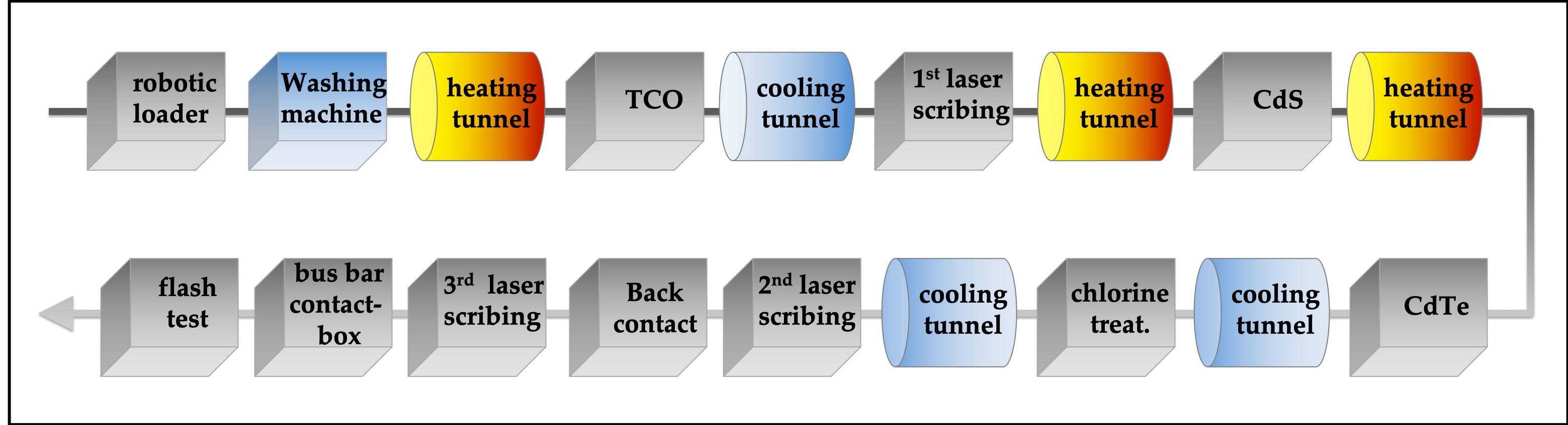
Cadmium telluride (CdTe) has achieved a truly impressive development that can commercially compete with silicon, which is still the king of the market. Solar cells made on a laboratory scale have reached efficiencies close to 22%, while modules made with fully automated in-line machines show efficiencies above 18%. Based on the research developed in our laboratory, the fabrication processes of both CdTe polycrystalline thin-film solar cells and photovoltaic modules are critically discussed. The most common substrates, the constituent layers and their interaction, the interfaces and the different “tricks” commonly used for obtaining highly efficient devices will be analyzed.
1. Introduction
Solar cells and photovoltaic (PV) modules have been intensively studied since the 1950s, when a Si-based p/n junction, able to convert sunlight into electrical energy, was made for the first time. Since then, many steps for obtaining more and more efficient devices have been made, both with laboratory-scale solar cells and with commercial PV modules.
Many different materials were studied, which gave rise to their respective technologies. Others have been abandoned due to the inability to obtain power conversion efficiencies (PCE) high enough to be used in large-scale industrial production, or because they did not produce devices that were sufficiently stable over time. Among the most successfully technologies are certainly those based on single- and multi-crystalline Si, widely used in terrestrial PV generators and multi-junctions based on GaAs technology, which are essentially used for space applications.
In addition to Si technology, alternative materials and production processes have been developed in order to easily realize solar devices. The research was pushed towards the optimization of the PCE/cost ratio, decreasing the amount of constituent materials and using easily available low-cost substrates, such as soda-lime glass, polymers or thin metallic foils. This was the beginning of the thin-film technology, which demonstrated its potential when a fully automated in-line machine produced the first PV module based on amorphous Si (a-Si). The success of this technology is mainly due to two other materials: CdTe and Cu(In, Ga)Se2 (CIGS) which, thanks to the high efficiency obtained in recent years both on laboratory scale and in large modules [3], have completely replaced a-Si. Currently, a-Si finds its principal use in consumer electronics, such as calculators, watches, toys and gadgets, while the PV market is almost completely governed by multicrystalline silicon (mc-Si), relegating thin film technology to a small percentage of the market. This is firstly due to the fact that Si technology was the first implemented at an industrial level, secondly thin film technology developed high-efficiency modules only in the last ten years, when the PV market was already well-established. However, thin film technology, with its CdTe and CIGS diamond tips, is gaining more and more space in the PV market due to its excellent performance and the over-time stability achieved in recent years.
2. Discussion
Recently, a CIGS-based solar cell world record efficiency of 23.35% was achieved by Solar Frontier [1] over a designated area of about 1 cm2. The use of Cu(In, Ga)(Se, S)2, together with a high-temperature heavy alkali (Cs) post-treatment of the absorber layer, results in a reduced defect density. The enhanced quality of the Cu(In, Ga)(Se, S)2 allows the opportunity to benefit from the effects of a wider absorber bandgap. Consequently, the reverse saturation current density decreases, producing an important enhancement in photovoltage and fill factor (FF), leading to the world record efficiency result. Today, CIGS technology, with an annual production of around 1.8 GWp, covers a market share of 1.9%, which is principally supported by three producers: Miasolè, Solibro and Solar Frontier. Within the past ten years, the photovoltaic world has realized that 20% efficiency is more than enough to guarantee the so-called grid parity, or to make photovoltaics widely competitive with traditional energy sources [2][3]. To significantly affect the world energy market, the production volume of photovoltaic modules must be a few terawatts/year (TW/yr). TW-scale production implies a correct availability of the constituent elements. For CIGS technology, the greatest risk is represented by the availability of indium (In), since it is even more widely used in expensive devices such as flat panel displays (FPD) [4][5]. In this condition, the estimates predict that the demand for In will exceed the supply, when CIGS manufacturing volumes will reach 100 GW/yr. From this point of view, it is mandatory to exploit other materials, whose constituents are more available on the earth crust. For example, we have to consider that the abundance of Cu, Zn, Sn, and Sulphur is 68, 79, 2.2, and 420 ppm respectively, which is considerably higher compared to that of In, Cd, Te of 0.16, 0.15, and 0.001 ppm, respectively.
Even CdTe is considered a very good material to serve as an absorber in solar cells, due to its direct energy gap (1.45 eV), which is nearly ideal for photovoltaic energy conversion, corresponding to the maximum of the solar spectrum. A CdTe-based solar cell could exhibit a photocurrent of 30.5 mA/cm2 when illuminated with 100 mW/cm2 sunlight, offering a theoretical maximum efficiency close to 30%. Historically, the best performances were typically obtained with heterojunction in which the n-type partner was cadmium sulfide (CdS). Some different attempts were tried when p-type CdTe single crystals were coupled with In2O3 [6], ZnO[7] or a very thin n-type CdTe layer [8], obtaining a 13.8% maximum efficiency. The success of this material was not obtained by means of single crystal but, on the contrary, by exploiting one of its best characteristics, namely the possibility to produce a complete solar cell by simply using thin-film technology. In fact, CdTe/CdS total thin film heterojunction led to a 6% efficiency solar cell and this result has been known since 1972 [9]. However, the psychological limit of 10% efficiency was overcome in the 1980s only after a heat treatment in chlorine atmosphere was applied to the CdTe/CdS stacked layers [10]. In the following ten years, devices with efficiency close to 17% were made by optimizing both the front and the back contacts[11]. This was followed by a period of stasis in photovoltaic performance, in part due to intrinsic difficulties, such as the impossibility of extrinsically doping polycrystalline CdTe thin films and partly due to the fact that many researchers have devoted their activities to the technological transfer of production processes from laboratory to industrial scale. Around 2010, the photovoltaic conversion efficiency began to increase again, reaching values close to 20% in a short time. The continuous increase in efficiency is largely due to the optimization of the layers making up the antireflecting coating (ARC), the transparent electrical contact and the window layer, as well as a careful choice of the glass substrate. This led to a substantial increase in the photocurrent, going from 26.1 mA/cm2 for a cell with 17.6% efficiency [12] to a 28.59 mA/cm2 photocurrent for a cell with 19.6% efficiency, corresponding to a rather modest increase in photovoltage [3]. Unfortunately, there aren’t any details in the literature concerning these remarkable results. However, it seems clear that the photocurrent increase is not only due to a very good optimization of the light harvesting, but also to an accurate management of the CdTe energy gap in order to extent the absorption to longer wavelengths. CdTe(1−x)(S, Se)x alloys show energy bandgap values smaller than CdTe when x ≤ 0.05, corresponding to a maximum increase in the cutoff wavelength of about 15 nm. The corresponding increase in photocurrent can be evaluated in 1 mA/cm2. Moreover, the use of a CdTe(1−x)(S, Se)x mixed compound reduces the lattice mismatch at the metallurgical junction, resulting in enhanced charge transport properties. In 2015, a solar cell based on a CdTe(1−x)(S, Se)x thin film exhibited a world efficiency record of (22.1 ± 0.5)%, showing the following parameters measured under the global AM 1.5 spectrum (1000 W/m2) at 25 °C: Voc = 0.8872 V, Isc = 31.69 mA/cm2, fill factor = 0.785 over a designated illumination area of 0.4798 cm2 [13][14]. The fabrication process of this solar cell is particularly suitable to be implemented in a large area, fully automated, in-line production. This is made possible by the electrical in-series integration of the cells directly inside the production process (monolithically integrated) by means of a robotic laser scribing. This technology realized a 11% efficient module in 2002 by depositing the CdTe thin film with the electrodeposition technique [15]. In the years 2010–2011, the number of factories able to produce tens of megawatts/years of CdTe modules were 10 units worldwide. The production was based on the close-spaced vapor transport (CSVT) or close-spaced sublimation (CSS) techniques for the deposition of the CdTe layer and an average module efficiency ranging from 10% to 12% was announced [16]. At the end of 2012 a 14.4% efficient device was reported, which became 16.1% at the beginning of 2013. In March 2014, a 17.5% efficient module was obtained, followed by a world efficiency record of (18.6 ± 0.5)% in 2015. The photovoltaic parameters of such a module, taken under the global AM 1.5 spectrum (1000 W/m2) at a cell temperature of 25 °C, are: Voc = 110.6 V, Isc = 1.533 A and fill factor = 0.742 over a designated illumination area of 7038 cm2 [14]. Commercial modules with an efficiency of 18.2% are now available on the market. First Solar, with a 2.4 GWp annual production, covers 2.3% of the market share.
References
- Philip Jackson; Dimitrios Hariskos; Roland Wuerz; Oliver Kiowski; Andreas Bauer; Theresa Magorian Friedlmeier; Michael Powalla; Properties of Cu(In,Ga)Se2solar cells with new record efficiencies up to 21.7%. physica status solidi (RRL) - Rapid Research Letters 2014, 9, 28-31, 10.1002/pssr.201409520.
- Morgan Bazilian; Ijeoma Onyeji; Michael Liebreich; Ian MacGill; Jennifer Chase; Jigar Shah; Dolf Gielen; Doug Arent; Doug Landfear; Shi Zhengrong; et al. Re-considering the economics of photovoltaic power. Renewable Energy 2013, 53, 329-338, 10.1016/j.renene.2012.11.029.
- J. Hernández-Moro; J.M. Martinez-Duart; Analytical model for solar PV and CSP electricity costs: Present LCOE values and their future evolution. Renewable and Sustainable Energy Reviews 2013, 20, 119-132, 10.1016/j.rser.2012.11.082.
- Andrea Feltrin; Alex Freundlich; Material considerations for terawatt level deployment of photovoltaics. Renewable Energy 2008, 33, 180-185, 10.1016/j.renene.2007.05.024.
- Björn A. Andersson; Materials availability for large-scale thin-film photovoltaics. Progress in Photovoltaics: Research and Applications 2000, 8, 61-76, 10.1002/(sici)1099-159x(200001/02)8:1<61::aid-pip301>3.0.co;2-6.
- T. Nakazawa; K. Takamizawa; K. Ito; High efficiency indium oxide/cadmium telluride solar cells. Applied Physics Letters 1987, 50, 279-280, 10.1063/1.98224.
- Julio A. Aranovich; Dolores Golmayo; Alan L. Fahrenbruch; Richard H. Bube; Photovoltaic properties of ZnO/CdTe heterojunctions prepared by spray pyrolysis. Journal of Applied Physics 1980, 51, 4260, 10.1063/1.328243.
- J. Mimila-Arroyo; Y. Marfaing; G. Cohen-Solal; R Triboulet; Electric and photovoltaic properties of CdTe pn homojunctions. Solar Energy Materials 1979, 1, 171-180, 10.1016/0165-1633(79)90065-0.
- Bonnet, D.; Rabenhorst, H. New results on the development of a thin film p-CdTe/n-CdS heterojunction solar cell. In Proceedings of the Conference Record of the 9th IEEE Photovoltaic Specialists Conference, Silver Springs, Atlantic City, NJ, USA, 2–4 May 1972.
- Hideaki Ohyama; Tetsuya Aramoto; Seiji Kumazawa; Hiroshi Higuchi; Takashi Arita; Satoshi Shibutani; Tuyoshi Nishio; Junji Nakajima; Miwa Tsuji; Akira Hanafusa; Takeshi Hibino; Kuniyoshi Omura; Mikio Murozono; 16.0% efficient thin-film CdS/CdTe solar cells. Conference Record of the Twenty Sixth IEEE Photovoltaic Specialists Conference - 1997 2002, null, 343-346, 10.1109/pvsc.1997.654098.
- J. Britt; C. Ferekides; Thin-film CdS/CdTe solar cell with 15.8% efficiency. Applied Physics Letters 1993, 62, 2851-2852, 10.1063/1.109629.
- Wu, X.; Keane, J.C.; Dhere, R.G.; Dehert, C.; Albin, D.S.; Dude, A.; Gessert, T.A.; Asher, S.; Levi, D.; Sheldon, P. 16.5% Efficient CdS/CdTe Polycrystalline Thin-Film Solar cell. In Proceedings of the17th European Photovoltaic Solar Energy Conference, Munich, Germany, 22–26 October 2001.
- First Solar Establishes New World Record for CdTe Efficiency . First Solar . Retrieved 2020-4-17
- Martin A. Green; Ewan D. Dunlop; Dean H. Levi; Jochen Hohl-Ebinger; Masahiro Yoshita; Anita Wing Yi Ho-Baillie; Solar cell efficiency tables (version 54). Progress in Photovoltaics: Research and Applications 2019, 27, 565-575, 10.1002/pip.3171.
- D. Cunningham; M. Rubcich; D. Skinner; Cadmium telluride PV module manufacturing at BP Solar. Progress in Photovoltaics: Research and Applications 2002, 10, 159-168, 10.1002/pip.417.
- Alessio Bosio; Daniele Menossi; Samantha Mazzamuto; Nicola Romeo; Manufacturing of CdTe thin film photovoltaic modules. Thin Solid Films 2011, 519, 7522-7525, 10.1016/j.tsf.2010.12.137.