1. Fe-Based Thin-Film Superconductors
High-T
c (T
c > 20 K) superconductivity in Fe-based superconductors [
21,
43] was discovered in 2008 by Watanabe et al. [
44]. Epitaxial iron-based thin-film superconductors [
45] of very high quality are crucial in the manufacture of iron-based superconducting gadgets, like the Josephson junctions [
46] and superconducting quantum interference devices (SQUIDs) [
18]. They are also utilised in emerging iron-based superconductive coated conductors with high critical current density (J
c) under powerful magnetic fields. Thin films are also needed for academic purposes to realise the intrinsic characteristics of iron-based superconductors as substantial bulk solitary crystals are not easy to grow for some iron-based superconductors. There are various families/groups in which iron-based superconductors can be put into. In this paper, we identify these families as,
LnFeAs(O,F) (where the
Ln is the lanthanide element), also called the 1111 group, doped
AeFe
2As
2 (where
Ae is an alkaline-earth element) also the termed 122 group, Fe
Ch (where
Ch is a chalcogen) also termed the 11 group, and the FeSe mono-layer film, also called the 11-mono layer group. Molecular beam epitaxy and pulsed laser deposition are the most common Fe-based thin film fabrication and growth mechanisms. Several thin-film synthesis and applications articles [
43,
47,
48,
49,
50,
51,
52,
53,
54] for iron-based thin-film superconductors have been published.
1.1. LnFeAs(O,F) Family
The first high-T
c iron-based superconductor to be discovered, with T
c 26 K, is LaFeAs(O,F). It was discovered by Kamihara et al. [
24,
55]. They also discovered low-temperature iron-based superconductors, including LaFePO, whose T
c is approximately 4K [
56], LaNiPO whose T
c is approximately 3 K [
26] and LaNiAsO whose T
c = 2.4 K [
24]. These discoveries were made during the group’s investigation of transparent p-type oxychalcogenide semiconductors like LaCuSO [
26]. The group managed to increase T
c to 55 K by replacement of a lanthanoid element (Ln) from Lanthanum to Neodymium [
57]. The
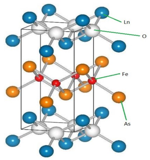
LnFeAs(O,F) family is called the “1111” group. The following
Figure 4 shows the LnFeAsO microstructure.
Figure 4. LnFeAsO structure.
The growth of LaFeAs(O,F) thin-films was first attempted by Hiramatsu et al. [
47]. Several processes such as reactive solid-phase epitaxy and simple pulsed laser deposition (PLD) growth were attempted to deposit the thin superconducting films of LaFeAs(O,F). Solid-phase epitaxy had been previously successful in growing LaZnOPn, but failed to produce satisfactory growth of LaFeAs(O,F). The breakthrough of getting the epitaxial films of LaFeAsO was brought by the simple pulsed laser deposition process (PLD). The Nagoya group employed molecular beam epitaxy (MBE) [
58,
59] and advanced the thin film growth of the 1111 compounds.
Backen et al. [
60] reported on the synthesis of LaFeAsO
1−xF
x superconducting film of polycrystalline by the ex-situ technique. They deposited the LaFeAsO
1−xF
x films on MgO and LaAlO
3 substrates by a pulsed layer deposition method. Annealing was then done at elevated temperatures in an evacuated silica-glass tube to obtain the superconducting thin films. The thin film transitioned into a superconducting state at approximately 11 K. The superconducting thin films showing a zero resistivity around the critical temperature of bulk samples were positively synthesised by reviewing the annealing state [
61].
Naito and Ueda et al. [
62] reported on the SmFeAsO (Sm1111) thin film on CaF
2 substrate synthesised by molecular beam epitaxy. The film transitioned into a superconducting state at around 56 K. This was somewhat higher than T
c of SmFeAs(O,F) bulk samples [
59,
62]. CaF
2 was first used by Tsukada et al. [
63] as a substrate in the deposition of FeSe
1−xTe
x. CaF
2 is effective in the manufacture of other iron-based superconductors, as evidenced by the enhancement of T
c in Sm1111 film [
62].
Haindl et al. [
64] grew superconductive Sm1111 films on CaF
2 substrates using pulsed layer deposition. They noted that SmFeAs(O,F) films synthesised on BaFe
2As
2-buffered MgO substrates by employing the SmFeAsO
0.9F
0.1 polycrystalline target had virtually identical lattice parameters with those of SmFeAsO bulk samples. They, however, exhibited a glitch, alleged to be a result of structural transition [
65], near a temperature of 150 K and no superconductivity in the temperature dependence of resistivity. These findings showed the insufficiency of the F content in this film. The Sm1111 film on CaF
2 substrate fabricated from the identical target transitioned into a superconducting state at 40 K.
1.2. Doped AeFe2As2 family
In the second group (doped
AeFe
2As
2 or (Ae,K)Fe
2As
2), usually termed “122” compounds [
66,
67] the one with the highest T
c of ~38 K is Ba
0.65K
0.35Fe
2As
2. The compounds in this group have the crystal structure of ThCr
2Si
2 type. There is an alternating stacking of tetrahedron Fe
2Pn
2 layers and plain Ae layers in this family of compounds [
21]. Pn is the pnictogen atom, it can either be As or Sb.
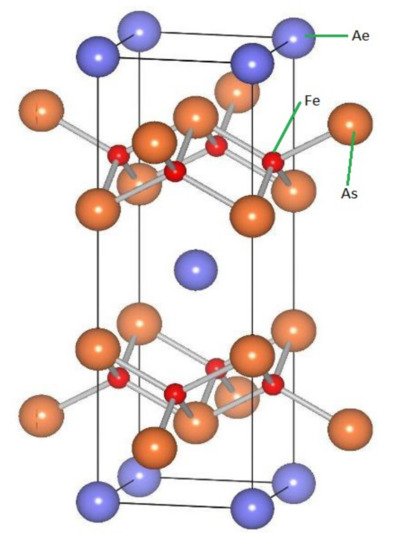
Figure 5 shows the
AeFe
2As
2 structure.
Figure 5. AeFe2As2 structure. The alternating stack of tetrahedron Fe2Pn2 layers and plain Ae layers can be seen in this structure.
Thin films of (Ae,K)Fe
2As
2 can be synthesised by using FeAs self-flux or Sn flux under ambient pressure. (Ae,K)Fe
2As
2 films growth is more difficult than LnFeAs(O,F) films. A group from Sungkyunkwan University synthesised superconductive (Ba,K)Fe
2As
2 films by a post-annealing method [
68,
69]. The TAT (Tokyo University of Agriculture and Technology) group synthesised thin films of (Ba,K)Fe
2As
2 and (Sr,K)Fe
2As
2 by molecular beam epitaxy [
70,
71,
72,
73]. Potassium is very volatile; therefore, it is not included in films grown at Ts > 400 °C. The TAT group worked on finding new superconductors and improving the T
c of Fe-based superconductors. Potassium-containing 122 films synthesis is performed at Ts ≤ 400 °C. The Fe-based superconductor Ba
1−xK
xFe
2As
2 is used as a key material for high magnetic field applications such as superconducting wires and bulk permanent magnets.
1.3. FeCh and FeSe Mono-Layer Film Family
In the family of Fe
Ch, also called the 11 compounds, divalent chalcogen ions surround the divalent Fe ions tetrahedrally. Fe
Ch structure is a sequential stacking of neutral tetrahedron Fe
2Ch
2 layer by van der Waals interaction. The Wu group [
74] discovered the superconductivity in FeSe (whose T
c is approximately 8.5 K) [
55,
75] and FeSe
0.5Te
0.5 (whose T
c is approximately 14 K) [
75] after the report on the unearthing of superconductivity in LaFeAs(O,F) by Hosono and his colleagues [
53]. The critical temperature of FeSe can be increased significantly when hydrostatic pressure is applied. It reaches 37 K at around 10 GPa [
76,
77].
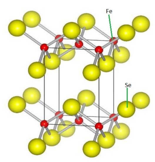
Figure 6 shows the structure of FeSe.
Figure 6. FeSe structure. Reddish brown balls are Fe atoms, while yellowish balls represent Se atoms.
The synthesis of group “11” iron-based thin films has been slow due to their toxicity [
21]. FeSe
1−xTe
x thin films growth was first realised by Wu et al. [
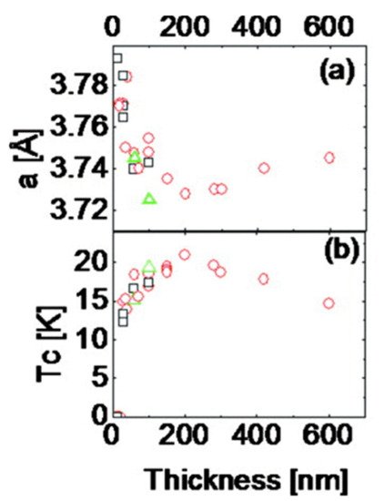
74] by a pulsed laser deposition technique. Bellingeri et al. [
78] reported that T
c in FeSe
0.5Te
0.5 thin films could be increased up to 21 K from around 14 K by varying thickness.
Figure 7 shows the thickness dependence of T
c that they reported.
Figure 7. Tc thickness dependence of FeSe0.5Te0.5 films. In (a) the thickness is plotted vs. lattice constant a [Å] while in (b) the thickness is plotted vs. Tc [K]. Structural analyses showed that the cfilm (=5.84–5.89 Å) is less than the bulk values (cbulk = 5.995 Å) though independent of the film thickness.
Hanzawa and his colleagues [
79] synthesised FeSe films, which were 100 Å thick on SrTiO
3 by molecular beam epitaxy. The highest T
c obtained was 35 K. Lei et al. [
80] conducted comparable experiments employing the flux method to grow FeSe single crystals.
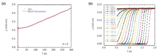
Table 1 summarises some of the transition temperatures of superconduction of the FeSe and Fe(Se,Te) thin films synthesised by molecular beam epitaxy and pulsed layer deposition.
Wang and his group [
82] detected large energy gaps that possessed superconducting properties using scanning tunnelling spectroscopy (STS) at low temperatures in mono-layer FeSe thin films on TiO
2-terminated STO (perovskite SrTiO
3) grown by molecular beam epitaxy. The U-shaped gap was found to have a magnitude of 40.2 meV at 4.2 K.
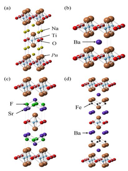
2. Layered Titanium Compounds
Layered titanium oxypnictides parent compounds are metallic without carrier doping, unlike cuprate superconductors [
93,
94,
95]. Hosono et al. [
48,
49] prepared the BaTi
2Sb
2O compound in 2012 and detected a bulk transition into superconductivity at a temperature of 1 K [
96]. Doan and his group [
97] autonomously presented an improved T
c of 5.5K in BaTi
2Sb
2O when it was doped with Na. BaTi
2Sb
2O was prepared via the solid-state reaction technique using very pure BaO, Ti, and Sb according to their stoichiometric ratios [
96]. This involved wrapping the specimen in a tantalum foil, sealing in a quartz tube and heating for a period of 40 h at an elevated temperature of 1000 °C. The sample was then cooled at a rate of 50 °C per hour up until room temperature was reached. The resulting compound had a tetragonal structure. X-ray diffraction and neutron diffraction data was used to determine the crystal structure of BaTi
2Sb
2O. It showed that the crystal structure is the same as that of BaTi
2As
2O [
98].
Figure 8 shows the various crystal structures of layered titanium compounds. The T
c of BaTi
2Sb
2O was found to be 1.36 K.
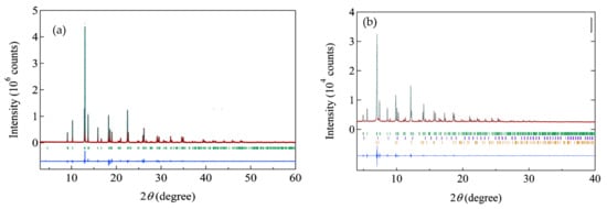
Figure 9 shows the synchrotron X-ray diffraction refinement results for BaTi
2Sb
2O and BaTi
2Bi
2O with the P4/mmm space group.
Figure 8. Crystal structures of different layered titanium compounds (
a) Na
2Ti
2Pn
2O, (
b) BaTi
2Pn
2O, (
c) (SrF)
2Ti
2Pn
2O, and (
d) (Ba
2Fe
2As
2)Ti
2As
2O [
54]. Pn is either Sb or As.
Figure 9. Refined synchrotron x-ray patterns of (
a) BaTi
2Sb
2O and (
b) BaTi
2Bi
2O. The Bragg reflection positions are shown by the green ticks [
54].
The Ti pnictide oxides BaTi
2Pn
2O (where Pn is Sb or Bi) contain layers of superconductive Ti
2Pn
2O and Barium blocking layers [
98]. Several titanium pnictide oxides have been produced. These include Na
2Ti
2Pn
2O (where Pn is As or Sb), (SrF)
2Ti
2Pn
2O (where Pn is As, Sb, or Bi), and BaTi
2Pn
2O (where Pn is As, Sb, or Bi). Amongst these compounds, only BaTi
2Pn
2O (where Pn is Sb or Bi) shows superconductive characteristics [
96,
97,
99,
100,
101,
102]. BaTi
2Sb
2O and BaTi
2Bi
2O were manufactured using the conventional solid-state reaction [
96,
98]. BaTi
2Bi
2O is unstable in air and some solvents, as it easily decomposes when exposed to air forming Bi-based phases such as BaBi
3 and Bi.
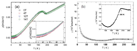
Figure 10 shows the resistivity and magnetic susceptibility of BaTi
2As
2O. The electronic structure of a compound is vital in understanding its superconductivity. The BaTi
2Sb
2O electronic structure as reported by Singh [
103] from first principles calculation showed that three d orbitals d
xy, d
x2−y2, and d
z2 have a substantial contribution at the Fermi level. This indicates that BaTi
2Sb
2O has a multiband nature. The oxygen 2p and Antimony (Sb) 5p are filled, while the Antimony 5p are hybridised with Titanium 3d. No Ba-derived occupied valence bands are present. The formal valence shown by the results is Ba
2+Ti
3+Sb
3−O
2−. The one 3d electron of Ti is responsible for the transport and magnetic characteristics of the composite [
95]. In the BaTi
2Bi
2O electronic structure, as reported by Suetin and Ivanovskii [
104], the three d orbitals have a substantial contribution at the Fermi level as is the case with BaTi
2Sb
2O.
Figure 10. (
a) The resistivity curve and (
b) magnetic characteristics of BaTi
2As
2O. The low-temperature enlarged scale magnetic field effect is shown by the inset in (
a) [
54].
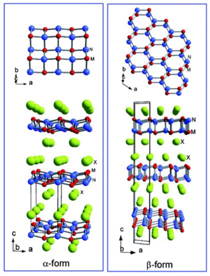
3. Intercalation Compounds with Layered and Cage-like Structures
Examples of high-temperature superconductors with layered or cage-like structures are cuprates [
105,
106], iron pnictides [
24,
44,
107], MgB
2 [
51,
108,
109] and alkali metal-doped fullerides [
54]. Their intercalated structures are made of charged (doped) layers attached to charge basins in the interlayer/cage-like space. There are two sub-families of layered polymorphs in metal nitride halides: the α-form and β-forms with stoichiometric formula MNX (where M is Ti, Zr, or Hf, N is Nitrogen and X is Cl, Br, or I). The α-form is an orthogonally MN layered network divided by halogen atoms, while the β-form contains dual honeycomb-like MN layers squeezed in between compact halogen layers [
110,
111]. MNX compounds are prepared by reacting the metal or metal hydride with ammonium halides at elevated temperatures [
112]. The chemical reaction is:
MNX compound was then ferried in a quartz glass tube with a little amount of NH
4X using a furnace whose temperature was between 750 and 850 °C. The resulting compounds were of α-form. The β-form was obtained by subjecting the α-form to a pressure of between 3 and 5 GPa at a temperature of around 800 °C. These superconductors have no magnetic ions, hence a magnetic pairing mechanism is not considered, but the possible candidates for the pairing mechanism have been assumed to be charge and spin fluctuations [
113,
114,
115].
Figure 11 shows the α- and β-form structures of the metal nitride halides.
Figure 11. Crystal structures of the α-form and the β-form of (where M is Ti, Zr, or Hf and X is Cl, Br, or I). The red atoms represent the metal (M) atoms; the blue are the Nitrogen atoms, and the green are halogen atoms (X).
When β-HfNCl is doped by intercalation of alkali metals, a high-temperature superconductor (T
c > 20 K) is obtained [
54]. Yamanaka et al. [
116] detected the highest T
c value of 25.5 K in the lithium and tetrahydrofuran (THF) co-intercalated superconductor Li
0.48(THF)
yHfNCl. Earlier, Yamanaka et al. [
117] found Zr homologue Li
xZrNCl to exhibit superconductive characteristics at T
c of approximately 14K. α-TiNCl required electron doping with alkali metals and organic bases like pyridine and alkylene diamines to be transformed into a superconductor [
54]. Magnetic susceptibility was conducted on the Lithium intercalated sample, Li
0.56HfNBr, from the chemical reaction with
n-BuLi in hexane. The following
Figure 12 shows the temperature dependence of the magnetic susceptibility of Li
0.56HfNBr.
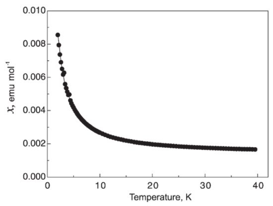
Figure 12. Temperature dependence of the magnetic susceptibility of Li0.56HfNBr. χ = C/(T − ϴ) + χ0. C is the curie constant and has the value of 0.0145(1) emu K mol−1, ϴ = 0.04(2) K and χ0 = 0.00126(1) emu mol−1.
There are also silicon clathrates and related compounds that have cage-like structures. High pressure and high temperature (HPHT) conditions can be used to prepare the Ba-containing silicon clathrate compound Ba
8Si
46. The compound displays superconductivity at T
c = 8.0 K [
110]. HPHT application is favourable for synthesising binary phases that are rich in Si such as LaSi
5, LaSi
10, BaSi
6, Ba
24Si
100, Ba
8Si
46, NaSi
6, Na
8Si
46, and Na
xSi
136 [
54,
110,
118,
119,
120]. Tanaka et al. [
121] synthesised Ca
2Al
3Si
4 using the HPHT method. The compound showed superconductive transition at T
c = 6.4 K.
4. Other Superconductors
In this group, we discuss the superconducting compounds that fall outside the previous categories already mentioned. These compounds fall into the low-temperature and high-temperature superconductors.
AM
2X
2-type (where M is not Fe) superconductors are an example of 122-type superconductors. Some non-Fe 122-superconductors have the ThCr
2Si
2-type structure and include compounds such as SrNi
2P
2 [
122], BaNi
2P
2 [
107], BaRh
2P
2, BaIr
2P
2 [
123], LaRu
2P
2 [
124], LiCu
2P
2 [
125], SrNi
2As
2 [
126], and BaNi
2As
2 [
127]. An example of 122-type antimonides and associated compounds is SrPt
2Sb
2 [
128]. Its measurements of electrical resistivity, magnetisation, and specific heat indicated a transition into superconductivity at T
c = 2.1 K. The compound was manufactured by Hosono et al. [
54] in two steps; arc melting and remelting of the specimen starting from Sr, Pt, and Sb. The superconductor is of Type II and has a lower critical field (H
c1) and upper critical field (H
c2) of 6 Oe and 1 kOe, respectively, at a temperature of 1.8 K [
54].
Cobalt-based superconductor LaCo
2B
2 [
129] was synthesised using the arc-melting technique for Lanthanum, Cobalt, Boron, Yttrium, and Iron mixtures. It was found to be superconductive after constituent cation isovalent or aliovalent substitution [
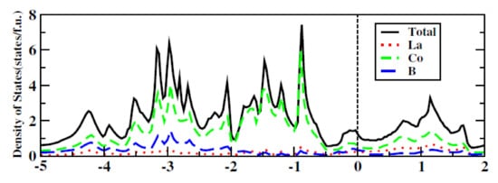
54]. Density Functional Theory (DFT) was used to investigate the electronic structure of LaCo
2B
2. From these calculations, it was confirmed that La ions take +3 state. It was also confirmed that the strong covalent CoB layer is responsible for metallic conduction. Pauli paramagnetic state results due to the suppression of the spin moment of the Co ion by this strong covalency [
54].
Figure 13 below shows the calculated Density of State (DOS) of the LaCo
2B
2 compound.
Figure 13. Calculated density of state (DOS) of LaCo2B2.
BaNi
2As
2 has a tetragonal ThCr
2Si
2 type crystal structure at room temperature [
127,
130,
131] and undertakes a transition of its structure at approximately 130 K to a triclinic structure where alternate Nickel-Nickel bonds are created in the Nickel plane. This new phase shows conventional BCS type superconductive characteristics below 0.7 K [
127,
131,
132,
133]. The BCS type superconductivity is based on the formation of Cooper pairs. The electron-electron interaction that results from virtual exchange of phonons is non-repulsive when the energy difference between the electrons states concerned is below the phonon energy. During pair formation, two electrons with opposite spin always combine with each other [
22]. One electron creates a positive charge fluctuation, which then attracts a second incoming electron behind it. This attraction continues creating a train of electrons. In the superconducting state, the two electrons interact via a phonon or lattice distortion forming a cooper pair. BaNi
2As
2 superconductivity can be enhanced through phosphorus doping, the transition temperature, which is lower than 0.7 K for the triclinic phase with
x less than 0.07, is increased to 3.33 K in the tetragonal phase with
x = 0.077. Hosono et al. [
54] grew single crystals of BaNi
2(As
1−xP
x)
2 by a self-flux method using mixtures of Ba, NiAs, Ni, and P.
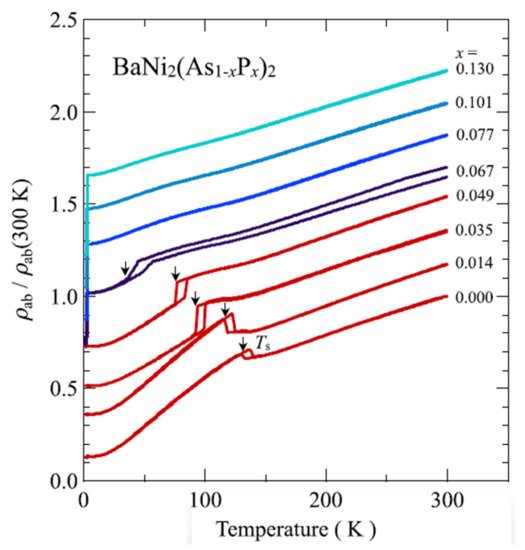
Figure 14 shows the temperature dependence of electrical resistivity parallel to the
ab plane.
ρab was normalised by the value at 300 K for BaNi
2(As
1−xP
x)
2. Phosphorus doping suppresses the triclinic phase, leading to the improvement of superconductivity.
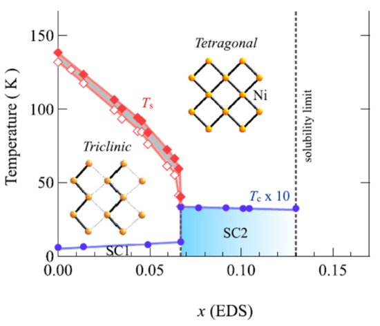
Figure 15 shows the BaNi
2(As
1−xP
x)
2 system phase diagram.
Figure 14. Temperature dependence of electrical resistivity parallel to the
ab plane for BaNi
2(As
1−xP
x)
2 crystal. The resistivity arnomally shown by thermal hysterisis in the figure shows tetragonal to triclinic transition [
134].
Figure 15. BaNi
2(As
1−xP
x)
2 system electronic phase diagram [
134]. SC1 and SC2 shows the phases of superconduction. Tetragonal-to-triclinic structural transition temperatures (Ts) upon cooling and heating are shown by open and closed diamonds, respectively. Ni planes in the triclinic and tetragonal phase are shown by the inserts.
Transition metal dichalcogenides MX
2 have two families; CdI
2-type telluride family and the pyrite (FeS
2)-type chalcogenide family [
54]. Self-flux technique was used to grow crystals of IrTe
2 [
135]. This involved mixing powders of Ir and Te at a ratio of 18:82 and placing it in a sealed alumina crucible and then placing it into a bigger quartz tube. After evacuating and sealing, the contents of the tube were heated to a temperature of around 1223 K for a period of 10 h, then increased again to 1433 K. The next step was to cool to 1173 K at a rate of between 1 and 2 K per hour. The final step was to quench the quartz tube in ice. At a temperature of around 250 K, IrTe
2 undergoes a transformation to a low temperature phase. The orbital degree of freedom is attributed to this transition since the Ir atoms’ d-orbitals are partially filled. Limited replacement of Platinum for Iridium in IrTe
2 overwhelms the creation of the low-temperature phase, ensuing the superconductivity incidence [
136,
137]. Its superconductivity appears for approximately 0.04 < x < 0.14 in Ir
1−xPt
xTe
2. The highest T
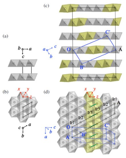
c of approximately 3.2 K is obtained at the trigonal and triclinic phase boundary when the x value is 0.04. When platinum is substituted, the Fermi level is shifted upwards. This affects the density of state near the Fermi level. The density of state is increased in the triclinic phase and decreased in the trigonal phase. The triclinic phase is also suppressed through the breakdown of the Ir-Ir dimers.
Figure 16 shows the crystal structure of IrTe
2 at different temperatures.
Figure 16. (
a,
b) The different views of the IrTe
2 crystal structure at 300 K. The trigonal lattice unit cell is shown by the black lines. (
c,
d) The IrTe
2 crystal structure at a temperature of 20 K. The blue and black lines show the triclinic lattice unit cell and the 5
a ×
b × 5
c supercell, respectively [
135], where
a, b, and
c are the high-temperature trigonal-cell parameters.
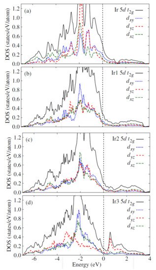
Figure 17 shows the computed orbital-decomposed partial density of state for the high-temperature trigonal phase and the low-temperature triclinic phase of IrTe
2. Ir2 dimers formation in the low-temperature phase yields strong bonding-antibonding splitting in the d
yz bands of the two Ir3 atoms. This makes the energy of the antibonding bands to increase above the Fermi level and reduces the energy of the bonding bands by 1 eV [
135].
Figure 17. The computed orbital-decomposed partial density of state for (
a) the high-temperature trigonal phase and the (
b–
d) low-temperature triclinic phase of IrTe
2. The dotted line is the Fermi level [
135].
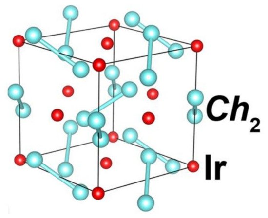
An example of the chalcogenide family of pyrite-type is Ir dichalcogenides Ir
xCh
2 (where Ch is Se or Te). The unit cell comprises of four Ir and eight Ch sites. The Iridium sites with haphazardly distributed vacancies make a simple fcc (face-centred-cubic) lattice structure. At times it assumes the pyrite-type structures when the Iridium site vacancies are introduced [
138]. High-pressure application effectively stabilises the pyrite-type form against the Cd
2I
2- type one [
139]. Qi et al. [
140] employed high-pressure synthesis technique to synthesise pyrite-type Ir
xCh
2 where the x value was near 1 and had transition temperature values of 6.4K and 4.7K for the two compounds Ir
0,91Se
2 and Ir
0,93Te
2, respectively. The density functional theory Qi et al. performed revealed that the compound consists of antibonding σ orbitals of the Se-Se dimer and dz
2 orbitals of the Ir. This meant that the transition from nonmetal to metal and the transition from metal to superconductor are driven by relaxation due to bond lengths which are alternating in the Se dimers array.
Figure 18 shows the pyrite structure of Ir
xSe
2.
Figure 18. Crystal structure of pyrite IrxSe2. The reddish-brown atoms are Ir, while the cyan colour represents Se atoms.
A noncentrosymmetric superconducting system [
141,
142,
143] contains a mixture of singlet and triplet states, called a mixed parity state. CePt
3Si [
144], CeCoGe
3 [
145], CeIrSi
3, and CeRhSi
3 [
146] are examples of this superconductor class. The last three superconductors have a BaNiSn
3-type structure.
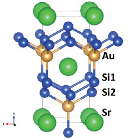
Many silicide superconductors are noncentrosymmetric, and most of them crystallise and show conventional s-wave superconductivity. The exclusions are the Cerium containing heavy-fermion compounds. Hosono et al. [
54] reported on two noncentrosymmetric silicide superconductors: SrAuSi
3 [
147] and Li
2IrSi
3 [
148]. SrAuSi
3 was the first noncentrosymmetric superconductor containing gold. Gold is a heavy element that causes strong spin-orbit coupling. The stability of the SrAuSi
3 superconductor was found only under high pressure [
147].
Figure 19 shows the crystal structure of SrAuSi
3. The green atoms are Sr, blue are Si atoms, and gold atoms represent Au. SrAuSi
3 is a relatively powerful coupling superconductor. Its T
c was approximated by the McMillan formula [
149,
150,
151], using the standard value of 0.13 for the Coulomb repulsion parameter μ*, resulting in a value of ∼19 K. SrAuSi
3 samples were synthesised using a high-pressure synthesis method at 6 GPa. The reactant powders of SrSi
2, Au, and Si were mixed in equal ratios in an agate mortar and then pressed into a disc which measured 6.9 mm in diameter, 3 mm in thickness, and weighed around 500 mg. The pellet was then placed in cell of high pressure (6 GPa), heated, and the temperature was kept at 1500 °C (1773 K) for an hour. Quenching to room temperature within a few seconds then followed.
Figure 19. Crystal structure of SrAuSi
3 [
147]. The structure is closely related to the ThCr
2Si
2 type and CaBe
2Ge
2 type structures.
Figure 20 illustrates the temperature reliance of resistivity quantified by fluctuating the magnetic field. The T
c of SrAuSi
3 at zero magnetic field is 1.6 K. As the magnetic field increases, T
c decreases. It gives H
c2(0), which is approximately 2.2 kOe. This value is way lower than the Pauli limit (H
p(0) of 30 kOe). Hosono et al. [
54] explain that the orbital pair breaking mechanism governs H
c2. There are several other non-Fe superconductors that have been reported, such as NbSiAs (T
c = 8.2 K) [
152], CeNi
0.8Bi
2 (T
c = 4 K) [
153], LaNiBN (T
c = 4.1 K), LaPtBN (T
c = 6.7 K), La
3Ni
2B
2N
3 (T
c = 15 K), La
2Sb (T
c = 5.3 K) [
153], Ba
n+2Ir
4nGe
12n+4 (T
c = 6.1 K for n = 1; T
c = 3.2 K for n = 2) [
154], Nb
4NiSi (T
c = 7.7 K) [
155], Ti
2O
3 [
156], and Ca
2InN (T
c = 0.6 K) [
157].
Figure 20. Illustration of the temperature reliance of resistivity quantified by fluctuating the magnetic field. (
a) The T
c of SrAuSi
3 at zero magnetic field is 1.6 K. (
b) As the magnetic field increases, T
c decreases. (
a) is taken over a wide temperature range while (
b) is on a narrow temperature range [
54].
Cuprates are another group of other thin film superconductors that we will discuss in this review. The cuprate superconductors can be fabricated by pulsed laser deposition (PLD), laser ablation and dc magnetron sputtering.
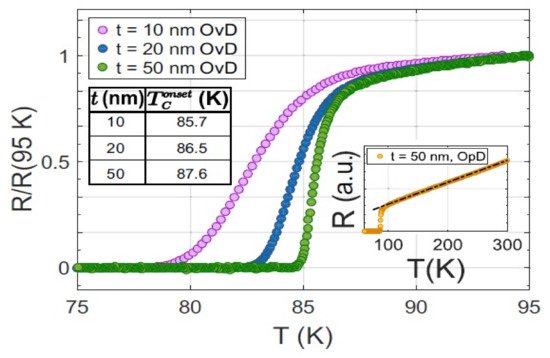
In 2017, Arpaia et al. [
158] reported on the fabrication of ultrathinYBa
2Cu
3O
7−δ (YBCO) films on a magnesium oxide substrate using the PLD technique from thicknesses ranging between 50 and 3 nm. Their deposition conditions were a temperature of 760 °C and an oxygen pressure of 0.7 mbar. After the deposition process, the deposited material was cooled at a rate of 5 °C/min. The group used atomic force microscopy (AFM) to perform morphological and structural characterisation. Scanning electron microscopy (SEM) and x-ray diffraction (XRD) were utilised to determine the film quality and structural properties, respectively. The team reported that the onset temperature of the superconducting transition slightly changes with the thickness of the film, while the zero-resistance temperature significantly decreases when reducing the film thickness. The lower onset transition temperature was attributed to both an increase and a decrease in oxygen doping in the film.
Figure 21 shows the temperature versus resistance curve of YBCO thin films where the thickness values are 10, 20, and 50 nm.
Figure 21. Resistance vs. temperature curve of YBCO thin films where the thickness values are 10, 20, and 50 nm. The insert table shows the values of the calculated onset transition temperature for the three thicknesses. The insert on the right shows the temperature versus resistance measurement of an optically doped 50 nm bare thin film whose onset transition temperature was 89.1 K [
158].
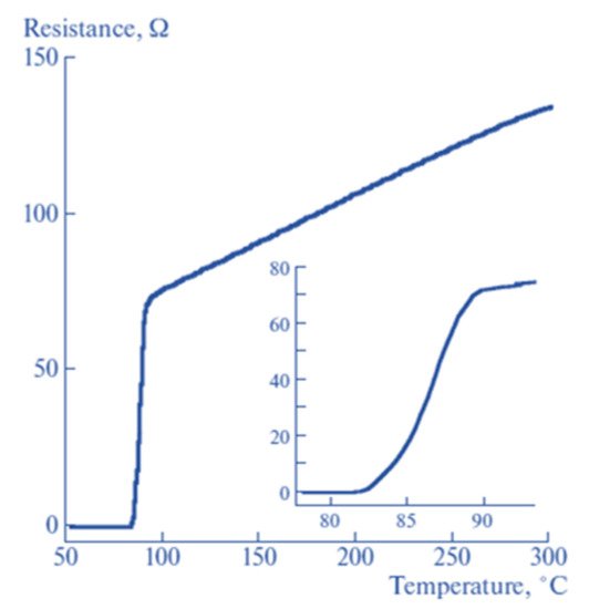
Stepantsov et al. [
159] reported on the growth of superconductive YBa
2Cu
3O
7−x thin films of b orientation on the surface of a SrLaGaO
4 crystal using the Czochralski technique. The team deposited a buffer layer of PrBa
2Cu
3O
7−x of 60 nm thickness onto the substrate surface using the rf sputtering technique. The chamber was filled with oxygen and argon gas mixture in a ratio of 1 to 4 up to a pressure of 0.1 mbars. The temperature of the substrate was raised to 600–750 °C while a 50 W rf discharge was applied between the target and the substrate. The chamber was then filled with pure oxygen to a pressure of 600 mbars and the substrate with the deposited film was annealed at 550 °C for an hour, after that it was cooled to room temperature. The chamber was then evacuated and replaced with a PLD chamber where the YBa
2Cu
3O
7−x was grown. The team reported that the film is free of any other domains of crystallographic orientations of the intrinsic material, which includes the a-oriented component.
Figure 22 shows the resistance vs. temperature curve for YBa
2Cu
3O
7−x.
Figure 22. Resistance vs. temperature curve of a b-oriented YBa2Cu3O7−x film grown on a substrate of SrLaGaO4.
Stepantsov et al. [
160] reported on the fabrication of superconductive YBa
2Cu
3O
7 thin-films with tilt CuO [
100] planes to the surface on SrTiO
3 substrate, using the pulsed laser deposition technique. The SrTiO
3 single crystals, which were prepared by the Verneuil technique, were x-ray oriented, cut, and polished by a chemical-mechanical method to obtain substrates with one of the [
100]—type planes tilted to the surface by 0 to 70° in 5° increments. YBa
2Cu
3O
7 was then grown on these substrates by PLD. The team used the four circle Philips X’Pert Xray diffractometer to study the structure of the films. They found that YBa
2Cu
3O
7 (YBCO) grown on the SrTiO
3 was a single crystal with the (014) face oriented parallel to the surface. They also reported that YBa
2Cu
3O
7 thin-films with CuO planes tilted to the surface by up to 41° can be deposited on the SrTiO
3 crystal surface [
160].
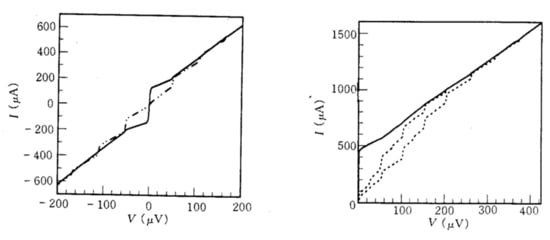
Kislinskii et al. [
161] reported on the production of direct current superconducting quantum interference devices (dc SQUIDS) and Josephson junctions using YBa
2Cu
3O
7 thin-films, which were deposited on ZrO
2 bi-crystal substrates stabilised by yttrium, using laser ablation and dc magnetron sputtering. The team used a strip with a width of 30 µm to measure critical transition temperature and critical density of the films. The strip had been patterned by chemical etching. The deposited thin films had a T
c of 90 K and critical current density of approximately 2 × 10
6 A/cm
2. The voltage modulation depth of this SQUID was 6 µV.
Figure 23 shows the voltage–current characteristic curves for the yttrium stabilised ZrO
2 and YBCO.
Figure 23. (Left) I–V characteristics of the Josephson junction on the 28° misoriented yttrium stabilised ZrO2 bi-crystal without (represented by solid line) and with microwave radiation of 23.4 GHz (represented by broken line) at a temperature of 77 K. (Right) I–V curves for the 28° misoriented weak link of YBCO at different levels of 23.4 GHz microwave power (dotted lines) and without radiation (solid line) at 62 K.
Carillo et al. [
162] reported on the resistance magneto-fluctuation measurements and proximity-effect in Nd
1.2Ba
1.8Cu
3O
z (NBCO) to analyse the coherent charge transport in the non-superconducting state. The team discovered an unanticipated inhibition of Cooper pair transport, and the disappearance of superconductivity when the temperature was lowered from 6 K to 250 mK. Their magnetoconductance and conductance measurements pointed to the mechanism of pair breaking at temperatures lower than 2 K. In their investigation, the team showed a transition of an underdoped NBCO nanostructure from a temperature above 2–3 K where Cooper pair transport is permitted, to a lower temperature where the Cooper pairs are not permitted to flow.
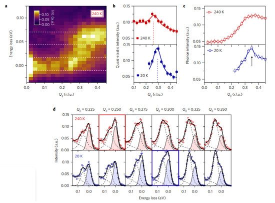
Chaix et al. [
163] reported on dispersive charge density wave excitations in Bi
2Sr
2CaCu
2O
8+δ. The team A new charge density wave (CDW) modulation was unearthed in underdoped Bi
2.2Sr
1.8Ca
0.8Dy
0.2Cu
2O
8+δ using ultrahigh resolution resonant inelastic X-ray scattering. Dispersive excitations were observed from an incommensurate charge density wave at low temperatures, which the enhanced phonon intensity. The CDW persisted near the pseudogap temperature, but other excitations drastically weakened, signalling a charge density wavevector shift. The phonon anomaly, dispersive CDW excitations and CDW wavevector analysis provided a momentum-space understanding of complex CDW behaviour.
Figure 24 shows the temperature dependence of the charge density wave and the phonon anomaly.
Figure 24. Temperature dependence of the charge density wave and the phonon anomaly. (a) RIXS intensity map taken at a temperature of 240 K. The quasi-elastic region (centred at zero energy loss) and the phonon energy region (centred at 60 meV) used for computing the mean intensity profile shown in (b,c) are defined by the white dashed line. (b) Averaged intensity of the quasi-elastic region (indicated in (a)) at 240 K (red) and 20 K (blue). The dashed lines indicate the position of the charge density wave. (c) Mean phonon energy regions intensity as defined in (a), at 240 K and 20 K. The black arrow highlights the intensity anomaly at 20 K. Error bars in (b,c) are estimated by the noise level of the spectra. (d) Raw energy-loss spectra (markers) and the corresponding fits (solid lines) of RIXS data taken at T = 240 K (at the top) and T = 20 K (at the bottom). Filled areas highlight elastic peak fits. Red and blue boxes for T = 240 K and T = 20 K, respectively, represent the RIXS spectra where the elastic peak intensity is maximal (that is, the CDW position).
This entry is adapted from the peer-reviewed paper 10.3390/pr10061184