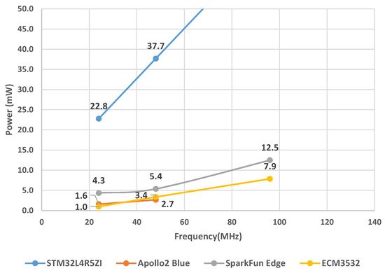
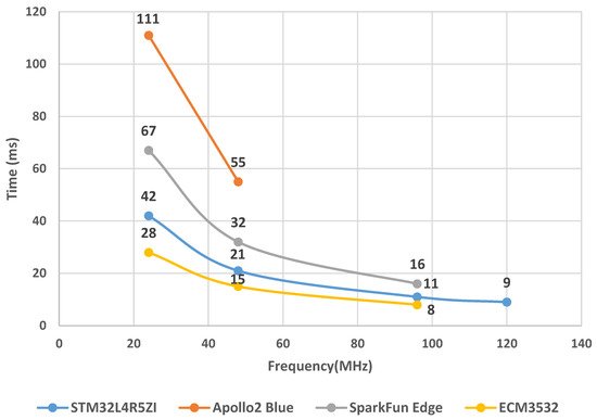
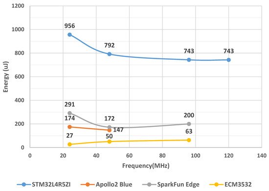
This paper investigates the energy savings that near-subthreshold processors can obtain in edge AI applications and proposes strategies to improve them while maintaining the accuracy of the application are investigated. The selected processors deploy adaptive voltage scaling techniques in which the frequency and voltage levels of the processor core are determined at the run-time. In these systems, embedded RAM and flash memory size is typically limited to less than 1 megabyte to save power. This limited memory imposes restrictions on the complexity of the neural networks model that can be mapped to these devices and the required trade-offs between accuracy and battery life. To address these issues, researchers propose and evaluate alternative ‘big–little’ neural network strategies to improve battery life while maintaining prediction accuracy.
- near-subthreshold processor
- energy efficient
- edge computing
- neural network
- adaptive computing
1. Introduction
2. Background and Related Work
In this section, reswearchers present an overview of current state-of-the-art hardware with power profiles in the order of 1 watt or less for edge AI and then algorithmic techniques and frameworks optimized to target this hardware.2.1. Hardware for Low-Power Edge AI
The high demand for AI applications at the edge has resulted in a significant increase in hardware optimized for low-power levels. For example, Google has delivered a light version of the Tensor Processing Unit (TPU) called Edge TPU which is able to provide power-efficient inference at 2 trillion MAC operations per second per watt (2TMAC/s/W) [3]. This state-of-the-art device is able to execute mobile version models such as MobileNet V2 at almost 400 FPS. The Cloud TPU focuses on training complex models, while the Edge TPU is designed to perform inference in low-power systems. Targeting significantly lower power than the Edge TPU, Ambiq released the Apollo family of near-threshold processors based on the 32-bit ARM Cortex-M4F processor. These devices can reach much lower energy usage measured at only 6 µA/MHz at 3.3 V under the working mode, and 1 µA/MHz at 3.3 V under sleep mode. The Apollo3 device present in the SparkFun board has 1 MB of flash memory and 384 KB of low-leakage RAM [4]. Similarly, Eta Compute has targeted energy-efficient endpoint AI solutions with the ECM3532 processor. This device is based on an ARM Cortex-M3 32-bit CPU and a separate CoolFlux DSP to speed up machine learning operations in an energy-efficient manner. The ECM3532 available in the AI vision board consumes less than 5 µA/MHz in normal working mode and 1 µA/MHz in sleep mode. According to Eta Compute, its implementation of self-timed continuous voltage and frequency scaling technology (CVFS) achieves a power profile of just 1 mW [5][6][5,6]. A characteristic of these near-threshold devices is that voltage scaling is applied to the core but it is not applied to the device’s SRAM/flash due to the limited margining possible in memory cells. Both Apollo3 and ECM3532 are based on the popular ARM architecture but, lately, the open-source instruction set architecture RISC-V has also received significant attention in this field. For example, GAP8 developed by GreenWaves Technologies features an 8-core compute cluster of RISC-V processors and an additional CNN accelerator [7]. The compute cluster is coupled with an additional ultra-low power MCU with 30 µW state-retentive sleep power for control and communication functions. For CNN inference (90 MHz, 1.0 V), GAP8 delivers an energy efficiency of 600 GMAC/s/W and a worst-case power envelope of 75 mW [7]. Other examples of companies exploring the near-threshold regime include Minima who has been involved in designs demonstrating achievable power savings [8]. Minima offers ultra-wide dynamic voltage and frequency scaling (DVFS) which is able to scale frequency and/or operating voltage based on the workload. This approach, combined with the dynamic margining approach from both Minima and ARM, is able to save energy by up to 15× to 20× [9]. The interest for adaptive voltage scaling hardware has resulted in a €100 m European project led by STMicroelectronics to develop the next generation of edge AI microcontrollers and software using low-power FD-SOI and phase change technology. This project aims to deliver the chipset and solutions for the automotive and industrial markets with a very high computing capacity of 10 TOPS per watt, which is significantly more powerful than existing microcontrollers [10].2.2. Algorithmic Techniques for Low-Power Edge AI
Over the years, different algorithmic approaches have appeared to optimize inference on edge devices with a focus on techniques such as quantization, pruning, heterogeneous models and early termination. The deep quantization of network weights and activations is a well-known approach to optimize network models for edge deployments [11][12][11,12]. Examples include [13], which uses extremely low precision (e.g., 1-bit or 2-bits) of weights and activations achieving 51% top-1 accuracy and seven times the speedup in AlexNet [13]. The authors of [14] demonstrate a binarized neural network (BNN) where both weights and activations are binarized. During the forward pass, a BNN drastically reduces memory accesses and replaces most arithmetic operations with bit-wise operations. Ref. [14] has proven that, by using their binary matrix multiplication kernel, the results achieve 32 times the compression ratio and improves performance by seven times with MNIST, CIFAR-10 and SVHN data sets. However, substantial accuracy loss (up to 28.7%) has been observed by [15]. The research in [15] has addressed this drawback by deploying a full-precision norm layer before each Conv layer in XNOR-Net. XNOR-Net applies binary values to both inputs and convolutional layer weights and it is capable of reducing the computation workload by approximately 58 times, with 10% accuracy loss in ImageNet [15]. Overall, these networks can free edge devices from the heavy workload caused by computations using integer numbers, but the loss of accuracy needs to be properly managed. This reduction in accuracy loss has been improved in CoopNet [16]. Similar to the concept of multi-precision CNN in [17], CoopNet [16] applies two convolutional models: a binary net BNN with faster inference speed and an integer net INT8 with relatively high accuracy to balance the model’s efficiency and accuracy. On low-power Cortex-M MCUs with limited RAM (≤1 MB), Ref. [16] achieved around three times the compression ratio and 60% of the speed-up while maintaining an accuracy level higher than the CIFAR-10, GSC and FER13 datasets. In contrast to CoopNet which applies the same network structures for primary and secondary networks, rwesearchers apply a much simpler structure for secondary networks in which each of them is trained to identify one category in the HAR task. This optimization results in a configuration that can achieve around 80% speed-up and energy-saving with a similar accuracy level across all the evaluated MCU platforms. Based on XNOR-Net, Ref. [18] constructed a pruned–permuted–packed network that combines binarization with sparsity to push model size reduction to very low limits. On the Nucleo platforms and Raspberry Pi, 3PXNet achieves a reduction in the model size by up to 38× and an improvement in runtime and energy of 25× compared to already compact conventional binarized implementations with a reduction in accuracy of less than 3%. TF-Net is an alternative method that chooses ternary weights and four-bit inputs for DNN models. Ref. [19] provides this configuration to achieve the optimal balance between model accuracy, computation performance, and energy efficiency on MCUs. They also address the issue that ternary weights and four-bit inputs cannot be directly accessed due to memory being byte-addressable by unpacking these values from the bitstreams before computation. On the STM32 Nucleo-F411RE MCU with an ARM Cortex-M4, Ref. [19] achieved improvements in computation performance and energy efficiency of 1.83× and 2.28×, respectively. Thus, 3PXNet/TF-Net can be considered orthogonal to ouresearchers' ‘big–little’ research since they could be used as alternatives to the 8-bit integer models considered in this research. A related architecture to researchers'our approach called BranchyNet with early exiting was proposed in [20]. This architecture has multiple exits to reduce layer-by-layer weight computation and I/O costs, leading to fast inference speed and energy saving. However, due to the existence of multiple branches, it suffers from a huge number of parameters, which would significantly increase the memory requirements in edge devices. The configuration of primary and secondary neural networks has been proposed for accelerating the inference process on edge devices in recent years. Refs. [17][21][17,21] constructed ‘big’ and ‘little’ networks with the same input and output data structure. The ‘big’ network is triggered by their score metric generated from the ‘little’ network. A similar configuration has also been proposed by [22], but their ‘big’ and ‘little’ networks are trained independently. ‘Big’ and ‘little’ networks do not share the same input and output data structure. Ref. [22] proposed a heterogeneous setup deploying a ‘big’ network on state-of-the-art edge neural accelerators such as NCS2, with a ‘little’ network on near-threshold processors such as ECM3531 and Apollo3. Ref. [22] has successfully achieved 93% accuracy and low energy consumption of around 4 J on human activity classification tasks by switching this heterogeneous system between ‘big’ and ‘little’ networks. Ref. [22] considers heterogeneous hardware, whereas reseaourchers' approach uses the ‘big–little’ concept but focuses on deploying all the models on a single MCU device. In contrast to how [22] deployed ‘big’ and ‘little’ models on the NCS2 hardware accelerator and near-threshold processors separately, rwesearchers deploy both neural network models on near-threshold MCU for activity classification tasks. A switching algorithm is set up to switch between ‘big’ and ‘little’ network models to achieve much lower energy costs but maintain a similar accuracy level. A related work [23] has performed activity recognition tasks with excellent accuracy and performance by using both convolutional and long short-term memory (LSTM) layers. Due to the flash memory size of MCU, reswearchers decided not to use the LSTM layers which have millions of parameters as shown in [23]. The proposed adaptive system is suitable for real-world tasks such as human activity classification in which activities do not change at very high speeds. A person keeps performing one action for a period of time, typically in the order of tens of seconds [24], which means that to maintain the system at full capacity (using the primary ‘big’ network to perform the inference) is unnecessary. Due to the additional inference time and computation consumed by the primary network, the fewer the number of times the primary network gets invoked, the faster the inference process will be and the lower the energy requirements [16][17][21][22][16,17,21,22].2.3. Frameworks for Low-Power Edge AI
Over the last few years, a number of frameworks have appeared to ease the deployment of neural network models on edge devices with limited resources. In [25], a framework is provided called FANN-on-MCU specifically for the fast deployment of multi-layer perceptrons (MLPs) on low-power MCUs. This framework supports not only the very popular ARM Cortex-M series MCUs, but also the RISC-V parallel ultra-low power (PULP) processors. The results in [25] show that the PULP-based ‘Mr.Wolf’ SoC can reach up to 7.1× the speedup with respect to a single core implementation and 13.5× the speedup over the ARM Cortex-M4. Moreover, by using FANN-on-MCU, a relatively big neural network with 103,800 MAC operations can be executed within 17.6 ms with an energy consumption of 183 µJ on a Nordic nRF52832 MCU with one ARM Cortex-M4. The same neural network applied on ‘Mr.Wolf’ with eight RISC-V-based RI5CY cores takes less than 1ms to consume around 50 µJ [25]. Similar to FANN-on-MCU, Ref. [26] delivers a fast deployment on the MCU framework called the neural network on microcontroller (NNoM) which supports more complex model topologies such as ResNet and DenseNet from Keras. A user-friendly API and high-performance backend selections have been built for embedded developers to deploy Keras models on low-power MCU devices. There are also deployment frameworks developed by commercial companies targeting low-power edge devices. For example, Google focuses on low-power edge AI with the popular TensorFlow Lite framework [27]. Coupled with the model training framework TensorFlow, Google can provide a single solution from neural network model training to model deployment on edge devices. STM32Cube.AI from STMicroelectronics [28] is also an AI deployment framework but it is only designed around the STM family devices such as STM32 Nucleo-L4R5ZI and STM32 Nucleo-F411RE. Eta Compute has created the TENSAIFlow deployment framework to provide performance and efficiency optimizations for Eta-series MCU products such as ECM3531 and ECM3532 [29]. In ouresearchers' methodology, the lack of support for certain devices in some frameworks means that researcherswe have combined tools from different vendors. ResearchersWe have applied frameworks from [26][27][29][26,27,29] for model deployments on MCUs such as ECM3532 and STM32L4.3. Low-Power Microcontroller Evaluation
Four commercially available microcontroller devices designed for energy-efficient applications from STMicroelectronics, Ambiq and Eta Compute are considered in this comparison. Table 1 shows the technical details of these four MCUs. Three of them (STM32L4R5ZI, Apollo2 Blue and SparkFun Edge (Apollo3 Blue)) are based on the Cortex-M4 microarchitecture with floating-point units (FPU) [4][30][31][4,30,31], while the ECM3532 is based on the Cortex-M3 microarchitecture with a ‘CoolFlux’ 16-bit DSP [5]. The 32-bit ARM Cortex-M3 and M4 are comparable microarchitectures both having a three-stage pipeline and implementing the Thumb-2 instruction set with some differences in the number of instructions available. For example, additional 16/32-bit MAC instructions and single-precision FPU are only available on the Cortex M4.| Devices | Manufacturer | Architecture | Embedded Memory (Flash/SRAM/Cache) | Clock Frequency | Core Voltage | Sleeping Mode Current | Work Mode Current | Power Scaling Capabilities |
|---|---|---|---|---|---|---|---|---|
| STM32L4R5ZI | STMicroelectronics | 32-bit Cortex-M4 CPU with FPU | 1 MB/320 KB | up to 120 MHz | 1.05 V | <5 µA with RTC | 110 µA/MHz | Dynamic voltage scaling with two main voltage ranges |
| Apollo2 Blue | Ambiq | 32-bit Cortex-M4 CPU with FPU | 1 MB/256 KB/16 KB | up to 48 MHz | 0.5 V | <3 µA with RTC | 10 µA/MHz | SPOT (Subthreshold Power Optimized Technology) |
| SparkFun Edge (Apollo3 Blue) | Ambiq | 32-bit Cortex-M4 CPU with FPU | 1 MB/384 KB/16 KB | up to 96 MHz (with TurboSPOT Mode) | 0.5 V | 1 µA with RTC | 6 µA/MHz | SPOT (Subthreshold Power Optimized Technology) with TurboSPOT |
| ECM3532 | Eta Compute | 32-bit Cortex-M3 CPU with 16-bit ‘CoolFlux’ DSP | 512 KB/256 KB/0 KB | up to 100 MHz | 0.55 V | 1 µA with RTC | 5 µA/MHz | CVFS (Continuous Voltage Frequency Scaling) with multiple frequency and voltage points |


