2. Metal Oxides and Photocatalysis
2.1. Fundamentals of Metal Oxides
Metal oxides belong to the group of semiconductor materials, which have chemical structures formed by the interaction of charges belonging to oxygen atoms (highly electronegative) with atoms of metallic elements. By definition, semiconductors have a structure composed of electronic bands, where the valence band (filled) is separated from the conduction band (unfilled) by a bandgap, with sufficient energy (around 1.0–3.0 eV) to maintain them with electrical insulators behavior at the temperature of 0 Kelvin
[16][17][16,17].
Metal oxides gained attention in the 1950s due not only to their potential to catalyze acid-base reactions, but to their potential participation with double acid-base sites in catalytic events (small regions that have the simultaneous participation of an acid and a base)
[18]. In general, the catalytic surface of metal oxides consists of anionic oxygen centers, as Lewis base sites (O
2−), and of coordinatively unsaturated cationic metal centers, as Lewis acid sites. Anionic oxygen centers have high electronegativity and can form ionic bonds when interacting with metals.
These materials can be produced through various industrial methods, such as chemical treatments of their precursor reagents, hydrothermal and precipitation reactions, sol-gel, sputter-coating, green synthesis, among others
[19].
With these synthesis routes, it is possible to produce metal oxides with particle sizes on the nanometric scale (of the order of 10
−9 m), which directly influences the increase in the surface area/volume ratio of these materials and, consequently, the greater efficiency in the application of these oxides as functional materials.
These materials present characteristics of conductors when they are excited by external environmental stimulus (such as light, pressure, electrical field, heat, magnetic field, etc.) with enough energy to allow electrons (e
−) of the valence band to migrate to the conduction band, jumping over the bandgap (consequently generating active holes (h
+) in the valence band)
[16][17][16,17]. In other words, their electrical and electronic properties are directly dependent on their electronic bands’ energy structure.
In this context, metal oxide nanostructures stand out in relation to other materials due to their synergistic combination between high superficial area/volume ratio and tunable optical, magnetic, electrical, mechanical, thermal, catalytic and photochemical characteristics, all resulting from their bulk and surface
[20]. These properties combined with their excellent chemical, structural and environmental stability, ensure them a variety of emerging applications, such as the production of electrochemical, optical and gas sensors, fuel cells, solar cells, piezoelectric devices, supercapacitors, adsorbents, photocatalysts, just to mention a few
[20][21][22][20,21,22].
The surface morphology of most metal oxides is critical in a variety of chemical processes. Metal oxides have been widely studied due to their optical, electronic, magnetic, electrical and mechanical characteristics, in addition to their high chemical stability and resistance to high temperatures (higher than the observed for polymeric materials), making them suitable for various applications in Science & Technology
[21].
Gas sensing
[23] and environmental remediation
[24] by means of photodegradation of organic dyes and heavy metals in aquatic media are examples of processes that can be performed and/or improved by enhancing metal oxides surface interaction with the media
[25].
When these materials are available in nanometric scale, they may present improved physical and chemical properties, such as adsorption capabilities, diffusion, surface area and modifiable surface functionalities, physicochemical stability, among others
[20][22][20,22].
Metal oxide-based nanocomposites (MON) are materials that are originated in the interaction between two or more metal oxides, or between metal oxides and other functional nanomaterials. Conducting polymers, metal nanoparticles and carbon-based materials are some examples of functional materials that are known to improve metal oxides properties
[22][26][27][22,26,27]. The main objective of this interaction is to provide enhanced attributes to the resulting material in comparison to those presented by single oxides, such as greater chemical/structural stability, lower bandgap, electron/hole recombination reduction, and greater contact area
[13].
The possibility of producing metal oxide-based nanocomposites with controlled size, morphology, composition, and interaction with other structures, will allow one to improve the just mentioned characteristics, opening simultaneously new perspectives for environmental applications, such as more efficient photocatalysis processes used for decontamination of aqueous media.
2.2. Electronic Structure
Metal oxides exhibit changes in their electrical/electronic properties based on variations in their crystalline structure, promoted by doping processes and/or external stimuli, such as electrical field, temperature, light, etc. These properties are based on the Band Theory (proposed by the physicist Felix Bloch, in 1928), which states that in a system with N identical atoms, each of the atoms orbitals gives rise to N new orbitals, thus forming a set of N levels with very close energy. The formed set is known as energy bands (
Figure 1a)
[28].
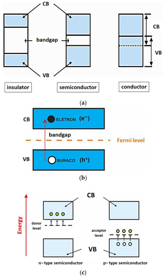
Figure 1. (a) Energy band model for insulating, semiconducting and conducting materials. (b) Illustration of the excitation of an electron from VB to CB, highlighting the generated charge carriers (e− and h+). (c) Energy bands of n−type and p−type extrinsic semiconductors.
According to this model, metal oxides as well as all other semiconducting materials possess two well-defined energy bands: the valence band (VB) and the conduction band (CB) (
Figure 1a). The band formed by the energy levels occupied by electrons, in the lower layers of the electronic distribution, is named the valence band, while the energy levels non-occupied by electrons in the higher layers form the conduction band. Between the VB and the CB, there is a quantum forbidden energy region (where no energy levels can be filled by electrons), called bandgap or forbidden band, which width is known as Eg. The energy dimension of this region determines whether a material is a conductor, semiconductor or insulator
[28][29][28,29].
In other words, the bandgap determines the minimum energy needed to excite the electrons from the VB to the CB, with a wavelength (λ) in the range of the ultraviolet–visible radiation spectrum
[30]. For insulating materials, the bandgap energy is greater than 5 eV and the density of free charge carriers in the CB is extremely low. In the case of semiconducting materials, the bandgap is much narrower (less than 5 eV): thus, they can change their condition from insulator to conductor by absorbing energy from irradiated photons, which possess energy greater than that of the bandgap. Consequently, VB electrons acquire enough energy that allows them to reach the CB (in the condition that they are free electrons, e
−), which provides the semiconductor characteristics of a conductive material
[28][29][28,29]. The excitation of an electron from the VB to the CB generates a hole (or hole, h
+) in the VB, which behaves like a positively charged particle. As a consequence, two charge carriers are generated, an electron (e
−) and a hole (h
+) (
Figure 1b): this phenomenon is known as photoexcitation
[31].
In these materials, photoexcitation can be hindered by electron/hole recombination. When recombination occurs, the hole is undone. On the other hand, the continuous incidence of an external stimulus on the material (a light source, for example), with energy greater than the bandgap of the material, can produce new holes in the VB, raising the electrons from the VB to the CB. Thus, it is possible to reduce the rate of the electron/hole recombination, therefore improving photocatalysis processes, for example, which directly depend on the interaction of the electric charge carriers with the contaminant molecule atoms.
Semiconductors can also be classified as intrinsic or extrinsic, due to the absence or presence of impurities in their crystalline lattice, respectively
[32]. Intrinsic semiconductors have the same amount of positive and negative carriers, since, for each electron that is promoted to the valence band, a hole is generated in the conduction band.
Thus, the electrical conductivity of the intrinsic semiconductor is defined by the product of the number of electrons and holes, by their respective charges and mobilities. Positive charges move in the same direction as the one of the electric field, while negative ones move in the opposite direction.
Another important concept for understanding the mobility of charge carriers in these materials is the Fermi energy level
[33], located in the bandgap region (
Figure 1b) of the semiconductors. The Fermi level represents the highest energy level, at absolute zero temperature, that an electron can occupy
[33]. For an intrinsic semiconductor, the Fermi level is exactly in the center of the bandgap. Extrinsic semiconductors are characterized by defects in the crystalline lattice (such as the absence of some atoms or their positioning outside the original position) and/or the presence of other elements through donor or acceptors doping (insertion of small amounts of substitutional atoms)
[34].
These defects allow energy levels in the bandgap to act as traps for charge carriers that are free in the crystalline structure, shifting the Fermi level position within the bandgap. Thus, the doping of a semiconductor with host atoms modifies the electronic distribution of electrons. For an extrinsic n-type semiconductor, the Fermi level shifts to a position just below the conduction band, whereas for p-type semiconductors, this level appears just above the top of the valence band
[35] (
Figure 1c, white balls represent holes and green balls electrons).
In the case of donor dopants (n-type semiconductors), atoms with a higher number of valence electrons are added (insertion of a group V atom into a crystal dominated by group IV atoms, for example). In this configuration, the semiconductor acquires an excess of electrons in relation to the number of holes. In this context, room temperature energy is sufficient for detaching an electron from the donor intermediate level (located in the bandgap), promoting it to the conduction band. In other words, the binding energy of the donor impurity is lower, which causes the donor energy level to be slightly below the conduction band of the host material. Analogously, in the case of acceptors (p-type dopants), atoms with less valence electrons are inserted (for instance, insertion of a group III element atom into a crystal composed essentially of group IV atoms). The absence of an electron Is treated as a hole In the valence band
[36].
This process alters the electronic density of the valence (p-type semiconductor) or conduction (n-type) bands: consequently, the new possibly occupied energy levels cause the bandgap energy to shrink, with a consequent increase in the electrical conductivity of the material. Siu’s work
[36] explains that the type and quantity of added impurities depends on the form and conditions of their growth, whether synthetically or naturally. In resume, by introducing impurities into the metal oxide crystalline network, it is possible to obtain an increase in the number of charge carriers and to improve the electronic properties of the final material for photocatalysis applications.
In the literature, several semiconducting metal oxides, such as titanium dioxide (TiO
2), zinc oxide (ZnO), tin dioxide (SnO
2), tungsten trioxide (WO
3), niobium pentoxide (Nb
2O
5), indium oxide (In
2O
3), cerium oxide (CeO
2) and graphene oxide have been explored, at the nanoscale level, for the development of functional photocatalysis devices
[13].
The state of the art on the subject confirms that the electronic and microstructural properties of metallic oxides-based photocatalysts devices were improved when used at their nanocomposite level: their synthesis at this level resulted from the interaction between two or more metal oxides or between metal oxides and other functional components/materials such as metal nanoparticles, conductive polymers or carbon materials. Sensors, fuel cells, supercapacitors, solar cells and photocatalysts are some of the examples of more recent technological applications for which significant enhancements were observed and reported
[37][38][37,38].
2.3. Metal Oxide-Based Photocatalysis
The term photocatalysis means to increase the kinetics of a photoreaction by the action of a catalyst. Photocatalysis is a photochemical process, of the advanced oxidative processes group, for the formation of free radicals, which are highly oxidizing and degrade organic substances in water.
Photocatalysis processes can be homogeneous or heterogeneous. The heterogeneous photocatalysis process differs from the homogeneous one, due to the former’s particularity of using catalysts in the solid state and, consequently, radicals are generated from the reactions between electron/hole (e
−/h
+) pairs with the medium, under the action of an incident light. This radiation is necessary for the homolytic breakdown of the oxidant to occur
[39]. The first heterogeneous photocatalysis processes emerged in the 1970s, through studies of photoelectrochemical cells, and aimed at producing fuel with low-cost materials
[40]. Fujishima and Honda in 1972
[40] described the oxidation of water containing TiO
2 in suspension, irradiated in a photoelectrochemical cell, which promoted the generation of hydrogen and oxygen. With the advent of nanotechnology and consequent advances in the development of new functional and environmentally friendly semiconductor materials, as well as of new techniques for characterizing and testing these devices, photocatalysis processes gained prominence as a viable alternative for applications in the domain of environmental decontamination, with high efficiency and reproducibility.
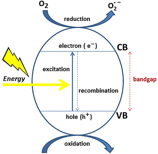
In the case of metal oxides-based systems, photocatalysis is established by a natural or artificial light stimulus. The HO
• and O
2•− species are photogenerated from the water molecules on the metal oxide surface and promote redox reactions capable of degrading contaminant molecules
[41].
The action of a metal oxide-based photocatalyst in an aqueous medium can be summarized as follows. First, the semiconductor is exposed to a light source, with enough energy to activate it: therefore, photons with energy greater than the energy of the bandgap are absorbed. This process causes an electron (e
−) to be transferred from the valence band to the conduction band, leaving a hole (h
+) in the valence band. Electrons (e
−) in CB react with the oxygen of the adsorbed water molecules at the oxide surface, forming superoxide (
𝑂2−) and/or hydroperoxide (
𝑂𝐻−) free radicals. Simultaneously, holes (h
+) generate HO free radicals from the adsorbed water at the metal oxide surface
[41]. An illustrative diagram of this process is represented in
Figure 2.
Figure 2.
Illustration of a metal oxide-based heterogeneous photocatalysis.
The combined action of direct redox processes, induced by holes and photogenerated electrons on the surface of the catalysts, and of indirect redox processes, derived from reactive oxygen species, is responsible for pollutant degradation
[13][42][43][13,42,43].
In short, the competition between the capacity for interfacial charge transfer and the recombination of the e
−/h
+ pairs, is a determinant factor for the photocatalytic efficiency of the materials. Basically, the action of free radicals leads to the degradation of contaminants in the form of carbon dioxide, H
2O molecules and salts of inorganic origin.
The main challenges of achieving photocatalysis with metal oxides are their high bandgap energies needed to overcome their recombination levels of electron–hole pairs and their chemical and structural stability. Several researchers have focused their work on the synthesis of narrow-band photocatalysts, which can be used under visible light irradiation. Various surface enhancement methods to achieve this include doping with metal/non-metal ions, surface interaction with other semiconductors, or the use of hybrid nanostructures with other functional semiconductors
[44][45][46][44,45,46].
The modification of the catalyst surface to restrict charge recombination and increase the visible light response through metal/non-metal doping has been extensively studied
[47], as discussed in the previous sections. As mentioned earlier, the doping of the semiconductor catalyst with metal ions can result in the formation of intermediate energy levels in the bandgap region and improve the separation of charge carriers
[48]. Between other advantages, the one that involves controlling the size of crystallites and of the surface area/volume ratio of the nanostructures must be referenced, once it will increase the adsorption of pollutants on their surface
[49].
In terms of photocatalytic performance and stability of the semiconductor materials, nanocomposites based on titanium dioxide (TiO
2), zinc oxide (ZnO), vanadium pentoxide (V
2O
5), niobium pentoxide (Nb
2O
5) and tungsten trioxide (WO
3) stand out
[50]. Metal oxide nanocomposites based on those oxides are widely studied for the reduction of organic pollutants due to their non-toxicity, high resistance to photo corrosion and availability in different crystalline forms with high photocatalytic activity
[51].
The applicability of hybrid nanocomposites based on TiO
2 anatase (which can result in materials with higher photoactivity and lower recombination rates) for removing contaminants has gained popularity due to their cost-effectiveness, allied with their surface properties, including morphology, surface area and adsorption affinity, and the possibility of absorbing visible light
[52][53][54][55][52,53,54,55].
On the other hand, the recovery and reuse of these nanocomposites in new decontamination processes may represent a limitation, especially regarding the separation of nanoparticles of the reaction medium after the end of the reaction. In this sense, different strategies have been applied to overcome these problems, such as the use of membranes able to support these metal oxide nanocomposites
[13].
Charge Transfer in MON-Based Photocatalysts by Surface Tailoring
For effective photocatalysis, the photocatalyst conclusively delivers charge carriers to the interface of the semiconductor electrolyte
[56][57][58][59][60][61][56,57,58,59,60,61]. Recently, some authors have explored surface interactions to improve photocatalytic activity, for instance, using nanomaterials with tailored structure that allows one to control the orientation of certain surfaces
[62][63][64][62,63,64].
Simultaneously, characterization techniques allowed one to look and understand more deeply the atomic structure of surfaces and their interaction with the environment
[65][66][65,66]. In consequence, it was possible to shape materials with metastable surface phases that possess enhanced electronic properties, while simultaneously fine tuning their photocatalytic reactivity. Evidence of surface orientation-dependent photocatalytic activity has been reported in literature. For instance, using polycrystalline thin films of rutile TiO
2, the photocatalytic reduction of Ag+ ions was investigated and a stronger photocatalytic activity of the {101}/{011} orientation of rutile TiO
2 was observed
[67].
Diverse mechanisms may contribute to the found surface reliance with photocatalytic reactivity. For example, if electrons and holes get diffused along different directions, diverse oxidation or reduction reactions will be exhibited by different surfaces of the crystalline structure. These differences can be due to the band structure, to polarization mechanisms, or to induced superficial electrostatic potentials caused by adsorption reactions.
Regarding band structure influence, which has its origin in the bulk properties of the materials, it was first proposed by Giocondi et al.
[68] that the differences in the photocatalytic activity on (110) and (100) surfaces of strontium titanate (SrTiO
3) was due to the bulk band structure, which caused anisotropic diffusion of photoexcited charge carriers. By close inspection of the band structure, the authors found that photoexcited electrons and holes had a momentum-vector in the h100i direction: consequently, excited charge carriers of the bulk get diffused mainly along the {100} surface, a fact used to explain the higher photocatalytic activity of this orientation.
As reported, controlling charge transport within the bulk can give rise to enhanced surface photocatalytic reactivity. However, as proposed for SrTiO
3, the diffusion of carriers through specific surfaces may not be just due to the band structure, but may also be the result of dipoles formation, inducing holes and electrons that diffuse in opposite directions.
In unpolarized ferroelectric materials, containing several domains with opposite polarity, but of which the total net polarization vector is zero, the photocatalytic reactivity of metallic salts was used to evaluate spatial distribution of photo-oxidation/-reduction reactions. It was shown that products originating from those reactions decorate the domain structure of some ferroelectric materials, such as BaTiO
3, after photo stimulation
[69][70][69,70]: it was observed that while photogenerated electrons led to the reduction of Ag+ ions with consequent distribution along the active surface of Ag clusters, photogenerated holes conducted to the oxidation and to the subsequent decoration of the active surface with lead oxide. Thus, electrons and holes diffusion is controlled by bulk polarization and transported along domains with opposing directions. By conducting and AFM analysis, Kalinin et al.
[71] defined domain patterns into the ferroelectric material, which subsequently was decorated by photoreaction resulting products.
Band bending in the near surface region can also promote direct charge transport. Photoexcitation causes electrons/holes to diffuse to the surface, promoting a down-ward/up-ward band bending near it. The generated electrical potential in the charged region enhances electron–hole separation with a consequent increase of the photocatalytic reactivity. Synthesizing, band bending is due to the created surface charges, induced by adsorption processes. Bhardwaj et al.
[72], when studying the photocatalytic activity of barium strontium titanate (Ba1-xSrxTiO
3), found a maximum in the activity for a tetragonal-to-cubic phase transition composition: they associated it with the anomalously high dielectric constant for this transition. If for different surface orientations the band bending varied, then strongly surface-dependent photocatalytic activities are generated.
Most photocatalytic reactions are carried in aqueous solutions. At the interface layer between the solution and the crystal, a charged double layer is formed, consisting of surface charges with a certain polarity, on the crystal side, and of ions with opposite polarity in the layer of the solution closest to the surface. This originates a potential barrier near the interface, which can be regulated by balancing the Fermi level of the immersed photocatalyst with the one of the electrolytes. Thus, it can be stated that photocatalytic activity depends on the potential barrier height: indeed, the height and width of the space-charged layer, which are determined by the potential barrier height, condition the electron–hole separation and diffusion to the surface. It must be pointed out that the potential drop in the interfacial layer affects ion transport along the solution into the material surface and thus, affects the photo-oxidation/-reduction of the ions at the surface. Bullard et al.
[73] studied and determined the pH value at which the surface carries no net charge for different rutile single crystals. They measured force–distance curves employing an atomic force microscope and used them to determine the pH values for which the curves shifted from attractive to repulsive. Strong surface-dependent pH-values were found for the studied activated surfaces.
In the literature, it was shown that the surface electronic properties of some photocatalysts based on transition metals are quite different from the ones found for the bulk. For instance, for the rutile TiO
2 (011) surface, a new metastable surface phase, not the typical shaped 2 × 1 one, was produced (it was experimentally confirmed that, under vacuum, one of the most common surfaces for rutile crystal, the (011) one, gets reconstructed into a 2 × 1 structure
[74]). This newfound phase, which displays a much smaller bandgap than that of bulk
[75], was characterized by scanning tunneling microscopy and spectroscopy (STM/STS) and photoemission spectroscopy. Indeed, it was found that the bandgap is only of around 2 eV, and that the majority of the bandgap narrowing was caused by the induction of new states on the top of the valence band of the bulk. This surface will attract holes, and consequently, it is expected that it will turn highly active regarding photo-oxidation reactions: as a consequence, electrons can transfer to other active surfaces, of the same particle, and make them available for photoreduction reactions. In summary, if the orientation of one surface can be modified by molding its bandgap, electron–hole separation processes would be boosted, and separate oxidation and reduction reactions would growth.
In a work by Lahiri et al.
[76], the growth of a monolayer of zinc sulfide (ZnS) over ZnO was used to enhance ZnO photocatalytic activity. Even if ZnO and ZnS both display a wide bandgap, the presence of a ZnS monolayer induces states on top of the ZnO valence band with a consequent upward band bending
[77]: similarly, as described for the new surface phase on TiO
2 (011)
[75], the formation of a similar hole-trapping layer is found for ZnO.
The phenomenon has also been observed in quantum dots/metal oxide-based nanocomposites, for the removal of toxic organic pollutants. Quantum dots (QD) are known as zero-dimensional (0-D) nanomaterials and have the peculiarity of having a very high surface area/bulk ratio. Photocatalysis processes with these materials can be improved in relation to the use of larger particles, since the electron–hole recombination is significantly reduced due to the short path for charge transfers from the crystal bulk interface to the surface of the nanocomposite
[64].
In summary, strategies that allow modifying surface electronic conduction characteristics will enhance not only the materials’ bulk properties but also the creation of charge-trapping layers at the materials surface.