 +1 credit
| Version | Summary | Created by | Modification | Content Size | Created at | Operation |
|---|---|---|---|---|---|---|
| 1 | P Susthitha Menon | + 3293 word(s) | 3293 | 2021-04-22 06:19:42 | | | |
| 2 | Karina Chen | -8 word(s) | 3285 | 2021-05-06 13:03:28 | | |
Video Upload Options
A photodetector converts optical signals to detectable electrical signals. Lately, self-powered photodetectors have been widely studied because of their advantages in device miniaturization and low power consumption, which make them preferable in various applications, especially those related to green technology and flexible electronics. Since self-powered photodetectors do not have an external power supply at zero bias, it is important to ensure that the built-in potential in the device produces a sufficiently thick depletion region that efficiently sweeps the carriers across the junction, resulting in detectable electrical signals even at very low-optical power signals. Therefore, two-dimensional (2D) materials are explored as an alternative to silicon-based active regions in the photodetector. In addition, plasmonic effects coupled with self-powered photodetectors will further enhance light absorption and scattering, which contribute to the improvement of the device’s photocurrent generation.
1. Introduction
Currently, the photodetector market is dominated by silicon-based photodiodes due to the matured fabrication process at low cost. Although silicon is an excellent and abundant semiconductor material, the narrow and indirect bandgap properties of silicon limit the detection spectrum, especially in the near-infrared region, which triggers the search for alternative materials, especially for optoelectronic applications [1]. Materials with wider bandgap such as ZnO, SiC and diamond are considered as better material choices due to advantages such as strong radiation hardness, good thermal and chemical stability as well as feasibility for harsh environmental applications. All these inorganic materials have high carrier mobility and excellent absorption coefficients but are restricted by high temperature synthesis, complex device fabrication and low flexibility. Those drawbacks were resolved by using organic materials but were limited by low carrier mobility. Therefore, hybridization between organic and inorganic material was proposed as a structure for photodetector and is being utilized to date [1][2]. The hybrid structure introduces heterojunctions in photodetectors that lead to built-in potential that can be used for self-powering application.
Photodetectors that are developed using non-2D materials only detect light at the ultraviolet spectrum, which limits their applications and development. Therefore, 2D materials are being extensively explored to push the performance limit further [3]. Intense exploration and examination in preparing stable 2D materials upon successful preparation of graphene led to the discovery of a 140 various different 2D materials with electronic properties from metallic to insulating [4][5][6]. The classes of 2D materials are X-enes, X-anes, Fluro-X-enes, transition metal dichalcogenides (TMDs), SMCs, MX-enes and other 2D materials, which are shown in Figure 1. Some examples of materials from the 2D materials family [4][7] are also illustrated in Figure 2.
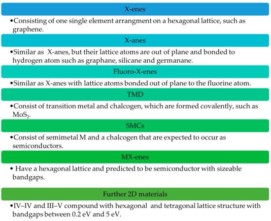
Figure 1. Classification of 2D materials (adapted from [4]).
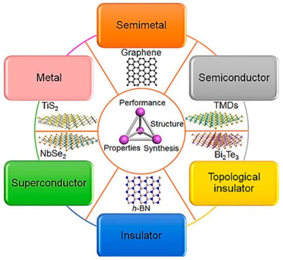
Figure 2. 2D material family (Reprinted from [7], with the permission of AIP Publishing).
Generally, 2D materials have great potential for high-performance photodetectors due to their high crystal quality and unique properties in both electronic and optical aspects such as tunable bandgaps with thickness variations [8], as well as strong covalent bonding between molecular layers with relatively low van Der Waals (vdW) at the interlayer [9]. Generally, 2D materials have large surface-to-volume ratios [10] with ultra-thin lattice structures [11] and flexible integrability [12]. Moreover, 2D materials are sensitive to light, heat and ambient, which make them suitable for broader spectrum detection from the infrared to ultraviolet regime [3][13][11]. Specific crystal structure and atomic layer stacking sequence, especially in TMDs, can vary the phases of 2D materials from the range of metallic, semiconducting, superconducting and insulating [14]. Nevertheless, 2D materials also have their limitations in terms of stability, speed, sensitivity, spectral selectivity and signal-to-noise ratio (SNR) [8]. Therefore, the requirement to meet these criteria were the motivation for studies related to improving the performances of 2D material-based photodetectors till present.
As mentioned earlier, there is a list of 2D materials that are being intensively studied for photodetection applications. However, this review highlights three main materials, which are graphene, MoS2 and h-BN with their heterostructures in terms of physics and electronic and optical properties. The integration of excellent electrical properties of graphene, especially in terms of ultra-fast carrier mobility and excellent optical properties of MoS2, in terms of large absorption coefficient and gain have been demonstrating significant enhancement in the performance of photodetectors. This is because the beneficial properties from both the materials were combined and the limitations of individual material were tackled by each other, which could contribute towards device performance. Despite intense research on these 2D materials in the past five years, the studies related to photodetectors with graphene and MoS2 heterostructures with/without h-BN were still being reported in 2020. The latest studies showed ultrahigh responsivity and detectivity via channel length reduction and Schottky barrier modulation [10], as well as impact of defect states towards photoresponse in graphene/h-BN/MoS2 photodetectors [15]. Although both the works did not specifically highlight the self-powering effect, their findings in I–V characteristics showed the potential of their approaches in self-powering application, where dark currents were suppressed and photocurrents were improved at zero biasing or low biasing approaching zero. The continuous exploration of device performance pertaining to graphene–MoS2 photodetectors in recent works is the motivation and rationale for selecting these materials in this review, as there is room for further investigation in terms of their device physics and fabrication approaches, which can result in improved photodetectors, especially with self-powering mechanisms.
This section covers briefly the properties of graphene, MoS2 and h-BN and focuses on the graphene/h-BN/MoS2 heterostructures in terms of device physics and working principles and device fabrication and highlights previous works on the performance of photodetectors with these heterostructures.
2. Graphene
Graphene is an sp2-hybridized carbon atom in a honeycomb lattice structure [16] that has a monoatomic layer thickness, high carrier mobility [17][11][14][18][19], broadband absorption from visible to infrared regime [17][11][18][19][20], high thermal conductivity [14], ultra-fast performance [21][20], high mechanical strength [14] and good toughness. It also has a gate tunability effect [17][19] and is a good candidate for high-frequency optoelectronics [11]. Graphene serves as a transparent electrode with high optical transmittance, large electrical conductivity and tunable work function. Monolayer graphene has 97.7% transparency, which decreases with increases in the number of layers at the visible light spectrum, and 2.3% white light absorption [3][13][14][22]. This limits graphene’s application in photodetectors in the pristine state [23]. Graphene behaves as a Schottky junction when combined with semiconductor materials for self-driven light detections [24][3][25]. The chemically-inert graphene is ideal as a contact electrode in the absence of diffusion and reaction with semiconductor crystals. It also has a tunable Fermi level to lower the contact resistance, which is a dominating problem in photodetectors, or even to create a barrier-free contact with semiconductors due to the finite density of the state of graphene [8].
Although graphene shows excellent properties for light detecting applications, it is limited by low photoresponsivity, detectivity and quantum efficiency due to its low light absorption coefficient and fast recombination rate [3] with an ultrashort photocarrier lifetime [26]. These drawbacks are due to the absence of a bandgap in graphene that makes it semi-metallic [17][11][14]. Many approaches were explored to tackle this issue, such as graphene bandgap opening with doping method, material engineering to enhance interaction between graphene and device structure engineering [27]. Moreover, the photogating approach can modulate the Fermi level in graphene, which can alter the behavior of graphene to be prone to either p-type or n-type when the Fermi level shifted either below or above the Dirac point, respectively. This will directly modulate the work function of pristine monolayer graphene, which is 4.5 eV. The modulation of the work function of graphene is also dependable to the interaction of graphene with its counterpart material in the device. Graphene was found highly p-doped, which resulted in a work function of 4.68 eV with Fermi level shifted 0.68 eV below the Dirac point, which could be contributed by the underlying substrate, adsorbates and polymer residue, as reported by Rathi et al. [28]. On the other hand, graphene in the self-powered photodetector that was studied by Li et al. showed an n-type behavior with Fermi level shifted 0.17 eV above the Dirac point, which was probably due to electron doping from multilayer MoS2 [29]. The tuneability of Fermi level in single layer graphene with respect to gate biasing and the effect towards resistivity is shown in Figure 3a. The presence of Fermi level at the Dirac point in a pristine graphene layer is shown in the inset of Figure 3a. Resistivity in the graphene layer is controlled based on the modulation of Fermi level, which is influenced by the gate biasing. The Fermi level is either lowered or raised from the Dirac point based on negative or positive gate biasing, which denotes the changes in behavior of graphene to be p-type and n-type, respectively. This reveals the ambipolar electric field effect in single layer graphene. The physics of Fermi level shifting is crucial, because it determines the carrier transport of the material, especially at the interface.
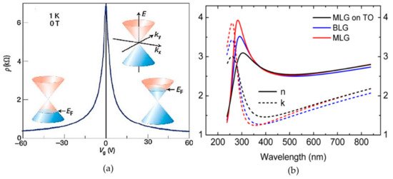
Figure 3. (a) Modulation of Fermi level with respect to gate biasing in single layer graphene. The inset shows a schematic of the band structure of pristine graphene with the presence of the Fermi level at the Dirac point (Reprinted from [16], with permission from Elsevier, 2010). (b) Refractive index and extinction coefficient for monolayer (red), bilayer (blue) and monolayer graphene with thermal oxide (black) (Republished with the permission of Royal Society of Chemistry, from [30]; permission conveyed through Copyright Clearance Center, Inc. (Danvers, MA, USA), 2015).
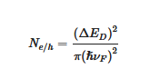
cm−2 with the carrier concentration of the electron and hole that can be calculated based on the linear Dirac-like dispersion relation, as in Equation (1) [31]. The Fermi velocity is given by νF=1.1×10⁶ m/s [32]. The carrier mobility, which is a superior property of graphene compared to other materials, was reported at an ultra-high value of 200,000 cm2/Vs for the mechanically exfoliated suspended layer [33]. However, the carrier mobility was reported to be 15,000 cm2/Vs for a graphene layer on silicon dioxide with a stable lattice structure at room temperature [3][34] due to the scattering effect. The carrier mobility of a graphene layer on a silicon dioxide substrate was recorded up to 40,000 cm2/Vs compared to a hexagonal boron nitride substrate, which reported carrier mobility up to 100,000 cm2/Vs [33]. This clearly shows that the carrier mobility of graphene also depends on the type of substrate.
 (1)
(1)
Besides electrical properties, optical properties of graphene were also studied in previous works [30][35]. The refractive index (n) and extinction coefficient (k) were evaluated for CVD-grown graphene. The n and k values for monolayer graphene, bilayer graphene and monolayer graphene with thermal oxide are shown in Figure 4 based on the work in [30]. The parameter of n determines the amount of light that is refracted when entering a material, while k indicates the amount of attenuation when light propagates through the material. On the other hand, the complex refractive index of mechanically exfoliated graphene was reported to be 2.4–1.0 i at 532 nm when measured by picometrology based on the work done in [35]. The optical parameter of k can be related to absorption coefficient through Equation (2), where α is the absorption coefficient in cm−1 and λ
is the wavelength of incident light.
 ()4πk
()4πkIn the context of a device, the optical responsivity of a graphene-based photodetector is usually poor, which was reported to be in the range of 1×10⁻² A/Wdue to limited light absorption at the atomically thin layer [8][19]. These limitations of graphene are being tackled by combining graphene with other materials, especially with 2D materials that form heterostructures, which is possible based on previous studies [17][19], including quantum dots/graphene, MoS2/graphene and WSe2/graphene heterojunctions in graphene-based photodetectors [8]. Moreover, chemical oxidation of graphene produces graphene oxide (GO), which shows the ability to absorb more light compared to a single layer of graphene at a micrometer thickness. The reduced graphene oxide (rGO) showed tunable carrier transport between electrons and holes dominant transport, in addition to tuning optical properties and bandgap for photodetection application [36]. Nitrogen-doped rGO (N-rGO), which was used to fabricate a photodetector with a metal–semiconductor–metal configuration had a reported photoresponsivity of 0.68 A/W at 1 V that was two orders of magnitude higher than pristine graphene [26], which also indicated the potential self-powering application due to excellent performance at low operating bias.
3. Molybdenum Disulfide (MoS2)
The family of TMDs gained most attention among 2D materials [14]. Generally, TMDs have hexagonal properties that absorb light at the visible to infrared spectrum [8]. They are promising semiconducting materials with ultra-thin bodies that enhance electrostatic gate control and carrier confinement with tunable bandgaps as well as diverse band-alignment with lack of surface dangling bonds [14]. This review emphasizes one of the famous and widely studied TMD materials, which is molybdenum disulfide (MoS2), which has Mo atoms sandwiched between two layers of S atoms and has natural availability with ambient/environmental stability [6][14].
MoS2 with a thickness of 0.65 nm at the monolayer [14] preserves more than 80% of it transparency, which is considered suitable for wearable applications by industry [32]. It appears as n-type material in nature [19] with the ability of light absorption at the range of visible to near-infrared [8], a large work function of 5.1 eV [37] as well as mechanically stability and transparency for flexible and transparent electronic systems [14]. The most attractive property of MoS2 is the adjustable bandgap from 1.2 eV to 1.8 eV when the material changes from the bulk condition to a monolayer, where it transforms from indirect to direct bandgap material, respectively, due to the quantum confinement effect. Therefore, MoS2 has thickness-dependable optical properties [13][15][38]. The bandgap changes from a single MoS2 monolayer to five layers and remains constant from five layer onwards, where it behaves as a bulk material [14][19]. Thus, it can be highlighted that the bandgap of MoS2 increases as the material thickness decreases. The electron affinity of MoS2 is also dependent on the number of layers. The electron affinity values that were reported for monolayer MoS2 were 4.0 eV [39], those of three layers of MoS2 were 4.0 eV [28] and those of multilayers (28 nm) were 4.1 eV [29]. All the values were obtained based on the fabricated devices.
The thickness of the MoS2 layer must be carefully chosen for optimum performance, based on application, because the thickness determines the contact Schottky barrier height (SBH), contact resistivity and carrier mobility [14]. SBH reduces from 0.6 eV to 0.3 eV when the thickness of MoS2 increases from a monolayer to five layers. Since reduced SBH is preferable for injection of charge carriers, a thicker MoS2 will suit this requirement, but a thicker structure is disadvantageous due to intercoupling resistance. Thus, the preferable thicknesses are in the range of 5 nm to 8 nm, which is about seven to twelve layers. The contact resistivity for MoS2 with thickness below five layers increased drastically due to quantum confinement-induced structure modification and increased slightly for thickness with five layers and above due to increments in the interlayer resistances. This clearly emphasizes again that the thickness of MoS2 must be selected carefully for optimum performance. Moreover, carrier mobility of monolayer MoS2 is lower in fewer layers because both the top and bottom surfaces are exposed to the environment that introduces scattering effect. The intrinsic electron mobility is highest in monolayer MoS2 because the effective mass of electron is reduced from 0.551 mo to 0.483 mo when MoS2 is thinned from bulk to the monolayer. Though the above reviews suggests that thicker MoS2 has better properties, it may not be practical for optoelectronic devices because they opt to utilize the direct bandgap nature that comes from the monolayer MoS2. Thus, an alternative approach is needed to tackle this issue, and the thickness of MoS2 must be tailored accordingly.
MoS2 with different thicknesses can tune the light absorption wavelength where a multilayer MoS2 phototransistor shows a wide spectrum of detection ranging from ultraviolet to near-infrared, as reported in [40]. As in the previous work by Li et al., the absorption coefficient for a few layers of MoS2 was reported to be 0.6 × 106 cm−1, and the incident light was mainly absorbed by this layer, which had a thickness of 28 nm because the absorption length was 17 nm [29]. Changes in photoconductivity, absorption spectra and photoluminescence occurred in MoS2 with the transformation from direct bandgap to indirect bandgap with variation in the thickness from monolayer to bulk, respectively [41]. The multi-layers of MoS2 with thicknesses of 150–165 nm, showed a better rectifying effect compared to MoS2 with a thickness ranging from 70 nm to 120 nm in dark condition [42]. Moreover, the large drain current at zero voltage indicated the presence of a photovoltaic effect, which can be attributed to the self-powering effect. The thickness of MoS2 is crucial because it influences the optical transparency of the material, which will contribute to the generation rate, as proven in [43][44] for solar cell applications. Optical transparency of MoS2 drops from 90% to 40% when the thickness of MoS2 is increased from a monolayer to six layers. However, in the context of MoS2/h-BN/graphene heterostructures, a multilayer MoS2 can establish a vertical depletion region to support tunnelling of photogenerated holes, which is a challenge in monolayer MoS2 due to an extremely thin vertical depletion region [29]. Therefore, the thickness of MoS2 layers, especially in a vertical device architecture, is a crucial parameter that must be tailored as it trades off the optical properties of the device, which will contribute to the performance of the photodetectors.
4. Hexagonal Boron Nitride (h-BN)
h-BN is an insulating 2D material that has a lattice constant 1.8% greater than graphene [45]. It is a 2D material that behaves as an insulator with bandgaps varying between 4.5 eV and 6 eV [33], and it has an approximately similar thickness and lattice structure to graphene, which enables both these materials to bind easily [29][13][12][33]. The insertion of h-BN in between graphene and MoS2 does not affect the electrical properties of the device at higher VDS (power supply voltage). However, a significant difference is observed when the voltage drops to zero bias. The photocurrent of the MoS2/graphene photodetector depresses at zero bias and approaches a similar value as the dark current. In contrast, the MoS2/h-BN/graphene photodetector demonstrates better photocurrent at zero bias due to the recovery of the photovoltaic effect. The ultra-thin h-BN layer acts as a barrier to hinder the interlayer transport of electrons, while photogenerated holes in MoS2 can tunnel through the ultra-thin h-BN. This recovers the internal electric field of the device [29].
The h-BN incorporation with semiconductor materials, especially with 2D materials, is being studied. The main focus of those research works pertains to studying the influence of h-BN materials on the entire device performance and tailoring the thickness of the h-BN layer to obtain optimum photocurrent with reduced dark current, which will later contribute to the photoresponsivity of the devices. This was proven based on the work in [12], where the thicknesses of h-BN flakes were in the range of 3–6 nm, and h-BN, with a thickness of 4 nm, was chosen to ensure an appropriate tunnelling barrier. This is because thicker h-BN layers lower the tunnelling under moderate biasing, whereas thinner h-BN layers contribute to larger leakage. A similar finding was proven in [23], where 5 layers of h-BN showed better power conversion efficiency (PCE) of 7.1% compared to 3 and 7 layers with PCE of 6.92% and 6.38%, respectively, in a graphene/h-BN/GaAs solar cell. Therefore, there is still plenty of room for research investigation regarding the thickness tailoring of h-BN, especially when interacting with different types of materials at both sides depending on the structure of insertion, which has contribution to improving the built-in potential of self-powering photodetection.
5. MoS2/h-BN/Graphene Heterostructures
Heterostructure devices based on vdW interactions combine the benefits from each material, and the internal built-in potential in the heterostructure can induce effective photogenerated carrier separation [8]. Therefore, a comprehensive summary regarding device physics and working principles, device fabrication and previous works involving graphene, MoS2 and h-BN heterostructures is covered in this section in order to understand the advances of these heterostructures in photodetection as well as to identify the research gap for further studies, especially in meeting the requirements for self-powering applications.
References
- Qin, Y.; Long, S.; Dong, H.; He, Q.; Jian, G.; Zhang, Y.; Hou, X.; Tan, P.; Zhang, Z.; Lv, H.; et al. Review of Deep Ultraviolet Photodetector Based on Gallium Oxide. Chin. Phys. B 2019, 28, 018501.
- Xie, Y.; Li, H.; Zhang, D.; Wang, Q.; Zhang, L. High Performance Blue Light Detector Based on ZnO Nanowire Arrays. Appl. Opt. 2019, 58, 1242–1245.
- Qiao, H.; Huang, Z.; Ren, X.; Liu, S.; Zhang, Y.; Qi, X.; Zhang, H. Self-Powered Photodetectors Based on 2D Materials. Adv. Opt. Mater. 2019, 8, 1900765.
- Schwierz, F.; Pezoldt, J.; Granzner, R. Two-Dimensional Materials and Their Prospects in Transistor Electronics. Nanoscale 2015, 7, 8261–8283.
- Nawz, T.; Safdar, A.; Hussain, M.; Lee, D.S.; Siyar, M. Synthesis, and Optoelectronic Device Application. Crystals 2020, 10, 902.
- Freedy, K.M.; McDonnell, S.J. Contacts for Molybdenum Disulfide: Interface Chemistry and Thermal Stability. Materials 2020, 13, 693.
- Li, X.; Tao, L.; Chen, Z.; Fang, H.; Li, X.; Wang, X.; Xu, J.B.; Zhu, H. Graphene and Related Two-Dimensional Materials: Structure-Property Relationships for Electronics and Optoelectronics. Appl. Phys. Rev. 2017, 4, 21306.
- Cui, Q.; Yang, Y.; Li, J.; Teng, F.; Wang, X. Material and Device Architecture Engineering toward High Performance Two-Dimensional (2D) Photodetectors. Crystals 2017, 7, 149.
- Kim, K.K.; Lee, H.S.; Lee, Y.H. Synthesis of Hexagonal Boron Nitride Heterostructures for 2D van Der Waals Electronics. Chem. Soc. Rev. 2018, 47, 6342–6369.
- Lee, I.; Kang, W.T.; Kang, W.T.; Kim, J.E.; Kim, Y.R.; Kim, Y.R.; Won, U.Y.; Lee, Y.H.; Yu, W.J. Photoinduced Tuning of Schottky Barrier Height in Graphene/MoS2Heterojunction for Ultrahigh Performance Short Channel Phototransistor. ACS Nano 2020, 14, 7574–7580.
- Sun, B.; Xu, J.; Zhang, M.; He, L.; Zhu, H.; Chen, L.; Sun, Q.; Zhang, D.W. Progress on Crystal Growth of Two-Dimensional Semiconductors for Optoelectronic Applications. Crystals 2018, 8, 252.
- Lu, Q.; Yu, L.; Liu, Y.; Zhang, J.; Han, G.; Hao, Y. Low-Noise Mid-Infrared Photodetection in BP/h-BN/Graphene van Der Waals Heterojunctions. Materials 2019, 12, 2532.
- Nalwa, H.S. A Review of Molybdenum Disulfide (MoS2) Based Photodetectors: From Ultra-Broadband, Self-Powered to Flexible Devices. RSC Adv. 2020, 10, 30529–30602.
- Rai, A.; Movva, H.C.P.; Roy, A.; Taneja, D.; Chowdhury, S.; Banerjee, S.K. Progress in Contact, Doping and Mobility Engineering of MoS2: An Atomically Thin 2D Semiconductor. Crystals 2018, 8, 316.
- Ahmed, T.; Roy, K.; Kakkar, S.; Pradhan, A.; Ghosh, A. Interplay of Charge Transfer and Disorder in Optoelectronic Response in Graphene/HBN/MoS2 van Der Waals Heterostructures. 2D Mater. 2020, 7, 025043.
- Bai, J.; Huang, Y. Fabrication and Electrical Properties of Graphene Nanoribbons. Mater. Sci. Eng. R. 2010, 70, 341–353.
- De Sanctis, A.; Mehew, J.D.; Craciun, M.F.; Russo, S. Graphene-Based Light Sensing: Fabrication, Characterisation, Physical Properties and Performance. Materials 2018, 11, 1762.
- Zhang, W.; Chuu, C.P.; Huang, J.K.; Chen, C.H.; Tsai, M.L.; Chang, Y.H.; Liang, C.T.; Chen, Y.Z.; Chueh, Y.L.; He, J.H.; et al. Ultrahigh-Gain Photodetectors Based on Atomically Thin Graphene-MoS2 Heterostructures. Sci. Rep. 2015, 4, 1–8.
- Roy, K.; Padmanabhan, M.; Goswami, S.; Sai, T.P.; Ramalingam, G.; Raghavan, S.; Ghosh, A. Graphene-MoS2 Hybrid Structures for Multifunctional Photoresponsive Memory Devices. Nat. Nanotechnol. 2013, 8, 826–830.
- Cakmakyapan, S.; Lu, P.K.; Navabi, A.; Jarrahi, M. Ultrafast and Broadband Graphene Photodetectors Based on Plasmonic Nanoantennas. In Proceedings of the 2017 IEEE MTT-S International Microwave Symposium (IMS), Honololu, HI, USA, 4–9 June 2017; pp. 1861–1864.
- Xu, H.; Wu, J.; Feng, Q.; Mao, N.; Wang, C.; Zhang, J. High Responsivity and Gate Tunable Graphene-MoS2 Hybrid Phototransistor. Small 2014, 10, 2300–2306.
- Nair, R.R.; Blake, P.; Grigorenko, A.N.; Novoselov, K.S.; Booth, T.J.; Stauber, T.; Peres, N.M.R.; Geim, A.K. Fine Structure Constant Defines Visual Transparency of Graphene. Science 2008, 320, 1308.
- Li, X.; Lin, S.; Lin, X.; Xu, Z.; Wang, P.; Zhang, S.; Zhong, H.; Xu, W.; Wu, Z.; Fang, W. Graphene/h-BN/GaAs Sandwich Diode as Solar Cell and Photodetector. Opt. Express 2016, 24, 134–145.
- Tian, W.; Wang, Y.; Chen, L.; Li, L. Self-Powered Nanoscale Photodetectors. Small 2017, 13, 1701848.
- Gonzalez Marin, J.F.; Unuchek, D.; Watanabe, K.; Taniguchi, T.; Kis, A. MoS2 Photodetectors Integrated with Photonic Circuits. NPJ 2D Mater. Appl. 2019, 3.
- Aniq, M.; Mohammad, S.; Hamizah, N.; Ari, Z.; Muhammad, S.; Ooi, P.C.; Syono, M.I.; Hashim, A.M. Wafer-Scale Fabrication of Nitrogen-Doped Reduced Graphene Oxide with Enhanced Quaternary—N for High-Performance Photodetection. ACS Appl. Mater. Interfaces 2019, 11, 4625–4636.
- Wang, J. Design Strategies for Two-Dimensional Material Photodetectors to Enhance Device Performance. InfoMat 2019, 1, 33–53.
- Rathi, S.; Lee, I.; Lim, D.; Wang, J.; Ochiai, Y.; Aoki, N.; Watanabe, K.; Taniguchi, T.; Lee, G.H.; Yu, Y.J.; et al. Tunable Electrical and Optical Characteristics in Monolayer Graphene and Few-Layer MoS2 Heterostructure Devices. Nano Lett. 2015, 15, 5017–5024.
- Li, H.; Li, X.; Park, J.H.; Tao, L.; Kim, K.K.K.; Lee, Y.H.; Xu, J.B. Restoring the Photovoltaic Effect in Graphene-Based van Der Waals Heterojunctions towards Self-Powered High-Detectivity Photodetectors. Nano Energy 2019, 57, 214–221.
- Wu, L.; Lu, P.; Bi, J.; Yang, C.; Song, Y.; Guan, P.; Wang, S. Structural and Electronic Properties of Two-Dimensional Stanene and Graphene Heterostructure. Nanoscale Res. Lett. 2016, 11, 1–9.
- Wang, J.; Ma, F.; Sun, M. Graphene, Hexagonal Boron Nitride, and Their Heterostructures: Properties and Applications. RSC Adv. 2017, 7, 16801–16822.
- De Fazio, D.; Goykhman, I.; Yoon, D.; Bruna, M.; Eiden, A.; Milana, S.; Sassi, U.; Barbone, M.; Dumcenco, D.; Marinov, K.; et al. High Responsivity, Large-Area Graphene/MoS2 Flexible Photodetectors. ACS Nano 2016, 10, 8252–8262.
- Abidin, N.F.Z.; Ahmad, I.; Ker, P.J.; Menon, P.S. Performance Characterization of Schottky Tunneling Graphene Field Effect Transistor at 60 Nm Gate Length. Sains Malays. 2017, 46, 1089–1095.
- Ochoa-Martínez, E.; Gabás, M.; Barrutia, L.; Pesquera, A.; Centeno, A.; Palanco, S.; Zurutuza, A.; Algora, C. Determination of a Refractive Index and an Extinction Coefficient of Standard Production of CVD-Graphene. Nanoscale 2015, 7, 1491–1500.
- Wang, X.; Chen, Y.P.; Nolte, D.D. Strong Anomalous Optical Dispersion of Graphene: Complex Refractive Index Measured by Picometrology. Opt. Express 2008, 16, 22105–22112.
- Wen, J.; Niu, Y.; Wang, P.; Chen, M.; Wu, W.; Cao, Y.; Sun, J.L.; Zhao, M.; Zhuang, D.; Wang, Y. Ultra-Broadband Self-Powered Reduced Graphene Oxide Photodetectors with Annealing Temperature-Dependent Responsivity. Carbon N. Y. 2019, 153, 274–284.
- Rahman, M.S.; Anower, M.S.; Hasan, M.R.; Hossain, M.B.; Haque, M.I. Design and Numerical Analysis of Highly Sensitive Au-MoS2-Graphene Based Hybrid Surface Plasmon Resonance Biosensor. Opt. Commun. 2017, 396, 36–43.
- Rashid, H.; Rahman, K.S.; Hossain, M.I.; Tabet, N.; Alharbi, F.H.; Amin, N. Prospects of Molybdenum Disulfide (MoS2) as an Alternative Absorber Layer Material in Thin Film Solar Cells from Numerical Modeling. Chalcogenide Lett. 2014, 11, 397–403.
- Vu, Q.A.; Lee, J.H.; Nguyen, V.L.; Shin, Y.S.; Lim, S.C.; Lee, K.; Heo, J.; Park, S.; Kim, K.; Lee, Y.H.; et al. Tuning Carrier Tunneling in van Der Waals Heterostructures for Ultrahigh Detectivity. Nano Lett. 2017, 17, 453–459.
- Ye, M.; Zhang, D.; Yap, Y.K. Recent Advances in Electronic and Optoelectronic Devices Based on Two-Dimensional Transition Metal Dichalcogenides. Electronics 2017, 6, 43.
- Wang, Q.H.; Kalantar-Zadeh, K.; Kis, A.; Coleman, J.N.; Strano, M.S. Electronics and Optoelectronics of Two-Dimensional Transition Metal Dichalcogenides. Nat. Nanotechnol. 2012, 7, 699–712.
- Zhong, X.; Zhou, W.; Peng, Y.; Zhou, Y.; Zhou, F.; Yin, Y.; Tang, D. Multi-Layered MoS2 Phototransistors as High Performance Photovoltaic Cells and Self-Powered Photodetectors. RSC Adv. 2015, 5, 45239–45248.
- Chaudhary, R.; Patel, K.; Sinha, R.K.; Kumar, S.; Tyagi, P.K. Potential Application of Mono/Bi-Layer Molybdenum Disulfide (MoS2) Sheet as an Efficient Transparent Conducting Electrode in Silicon Heterojunction Solar Cells. J. Appl. Phys. 2016, 120, 013104.
- Zhao, Y.; Ouyang, G. Thickness-Dependent Photoelectric Properties of MoS2/Si Heterostructure Solar Cells. Sci. Rep. 2019, 9, 1–11.
- Palla, P.; Uppu, G.R.; Ethiraj, A.S.; Raina, J.P. Bandgap Engineered Graphene and Hexagonal Boron Nitride for Resonant Tunnelling Diode. Bull. Mater. Sci. 2016, 39, 1441–1451.

