+1 credit
| Version | Summary | Created by | Modification | Content Size | Created at | Operation |
|---|---|---|---|---|---|---|
| 1 | Denzel Bridges | + 1991 word(s) | 1991 | 2021-02-24 03:27:46 | | | |
| 2 | Denzel Bridges | + 3 word(s) | 1994 | 2022-07-07 14:29:09 | | |
Video Upload Options
Nanojoining is the process of joining two or more surfaces together using nanomaterials as the primary building blocks. This includes, but is not limited to, nanosoldering, nanobrazing, nanowelding, nanoscale diffusion bonding, and additive manufacturing. Note that, like with conventional soldering and brazing, only the filler metal undergoes melting, not the base material. Nanomaterials are materials in which at least one dimension 100 nm or less and include 0-D (e.g. nanoparticles, 1-D (e.g. nanowires and nanorods), 2-D (e.g. graphene), and 3-D (e.g. nanofoam) materials. Nanomaterials exhibit several notable properties that allow joining to occur at temperatures lower than the melting temperature of their bulk counterpart. For example, the melting temperature of Ag is 961.78 °C, but Ag nanomaterials begin to melt at a much lower temperature that is dependent depending on the size and shape. These properties include high surface area to volume ratio, the Gibbs-Thompson effect, and high surface energy. The low joining temperature of nanomaterials has been exploited numerous times for flexible electronics, printable electronics, and soldering applications; only within the last two decades have they been explored for high-temperature joining applications (>450 °C).
1. Introduction
Nanojoining involves the use of nanomaterials (NMs; <100 nm) as a filler metal [1]. Particle-based joining allows additional freedom when working with processes such as additive manufacturing, printable electronics, and crack repair[2]. Nanoparticles have been so attractive as a lower temperature alternative to many conventional materials due to several unique properties. The first of which is size-dependent melting point depression of nanoparticles (NPs) seen in Figure 1. This melting point depression is caused by the Gibbs-Thomson effect [3]. The equation governing the Gibbs-Thomson effect (Equation 1) describes the melting point for an isolated spherical particle (\( T_{MP} \)) with a diameter, d.
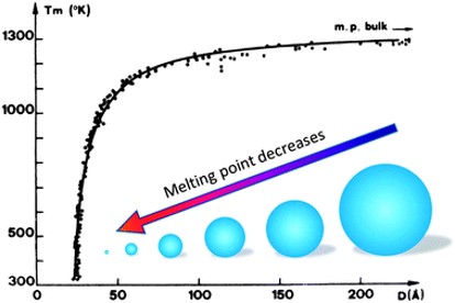
Figure 1: Melting point depression diagram of Au NPs [4]
\( T_{MP}(d)=T_{mB}(1-\dfrac{4\sigma_{sl}}{H_{f}\rho_{s}d}) \) (1)
\( T_{mB} \) is the bulk melting temperature, \( \sigma_{sl} \) is the solid-liquid interface energy, \( H_f \) is the bulk enthalpy of fusion and \( \rho_{s} \) is the molar volume of the solid. At this time, there has not been a firmly established Gibbs-Thomson equation for nanowires, nanoplates, and other non-spherical nanomaterials [5]. The Gibbs-Thomson equation was derived by equating the chemical potential of a liquid at \( T_m \) is equal to the chemical potential of a solid at \( T_m \) and a change in chemical potential occurs when the melting point changes [6]. The liquid drop model is another method used to approximate the melting point of NPs (Equation 2).
\( T_{MP}(d)=T_{mB}(1-\dfrac{6\nu_{o}\gamma_{sv}}{0.0005736T_{mB}d}) \) (2)
\( \nu_{o} \) is the atomic volume and \( \gamma_{sv} \) is the solid-vapor interfacial energy . Makkonen et al. discuss several methods for determining the different surface energies in the Gibbs-Thomson and liquid drop models [5]. Qi and Wang improved upon the liquid drop model by taking particle shape into account [7].
\( T_{MP}(d)=T_{mB}(1-\dfrac{6\alpha r}{d}) \) (3)
\( r \) is the atomic radius and \( \alpha \), in this equation, is a nanoparticle shape factor.
In addition to lower melting temperature, NPs also can experience surface melting and sintering, both of which occur at temperatures lower than the particle melting temperature. Surface melting occurs when the surface layer(s) of atoms is in a liquid or quasi-liquid state [3]. According to the Chernyshev model, surface melting can occur several hundred Kelvin below even the \( T_{MP} \) [8] (Equations 4-7).
\( T_{SM}(r)=T_{mB}[1+y(r)exp(-y(r))](0.75\alpha)^{-1} \) (4)
\( \alpha=\frac{2S_{vib}}{3R}+1 \) (5)
\( y(r)=\frac{\alpha-1}{\frac{r}{r_c}-1} \) (6)
\( r_c=3h(1+(\frac{0.75\alpha-1}{\alpha-1})^{-1}) \) (7)
\( S_{vib} \) is the bulk vibrational entropy of melting, \( R \) is the ideal gas constant, \( r_c \) is the critical radius under which surface melting does not occur, and \( h \) is the atomic diameter. This model assumes the surface layer is three atomic layers thick and that surface melting occurs when the NP surface is in a quasi-liquid state. Chernyshev's model is unresponsive to particles <10 nm in diameter [8].
Even lower than the surface melting temperature, NPs have a sintering temperature that can be 10-30% of the bulk melting temperature as seen in Equation 8 [9][10].
\( T_{s}(r)=0.3T_{mB}exp[-\dfrac{2S_m^{bulk}}{3k(\frac{r}{3h}-1)}] \) (8)
\( T_s \) is the sintering temperature, \( S_m^{bulk} \) is the bulk melting entropy, and \( h \) is the atomic diameter [11]. Sintering is a process in which adjacent particles are coalesced through solid-state (solid-state sintering) and/or liquid state diffusion (liquid-phase sintering). Note that sintering is an ongoing process once the minimum sintering temperature is reached and effective particle radius will continue to grow, thereby increasing the sintering temperature. When most researchers refer to sintering, they are referencing solid-state sintering unless otherwise stated.
Lastly, due to the lower activation energy required for diffusion in NPs, the diffusion coefficient for nanoparticles increases nonlinearly as particle size decreases. The Arrhenius-type equation that describes this as follows:
\( D(r,T)=D_oexp[\frac{-E_r}{RT}] \) (9)
\( E(r)=E_{bulk}exp[\frac{-2S_{vib}}{3R(\frac{r}{r_s}-1)}] \) (10)
\( D_o \) is the pre-exponential factor, \( E(r) \) is the activation energy of diffusion as a function of radius \( r \), \( R \) is the ideal gas constant, \( E_{bulk} \) is the bulk activation energy of diffusion and \( r_s \) is the radius of a NP if all atoms are located on the surface[12]. This relationship applies to lattice diffusion, grain boundary diffusion, and surface diffusion which are illustrated in Figure 2. The normal Arrhenius-type equation for bulk diffusion is expressed in Equation 11.
\( D(r,T)=D_oexp[\frac{-E_bulk}{RT}] \) (11)
\( D_o \) and \( E_{bulk} \) are typically determined by plotting the natural logarithm of the measured diffusion coefficient versus the reciprocal of the temperature in Kelvin. The y-intercept and slope multiplied by R of this plot are the \( D_o \) and \( E_{bulk} \), respectively (Figure 3).
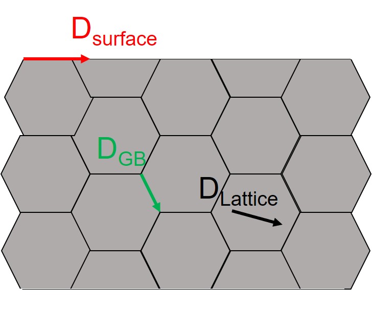
Figure 2: Illustration of three primary diffusion types lattice diffusion (\( D_{Lattice} \)), grain boundary diffusion (\( D_{GB} \)), and surface diffusion (\( D_{Surface} \)) [1]
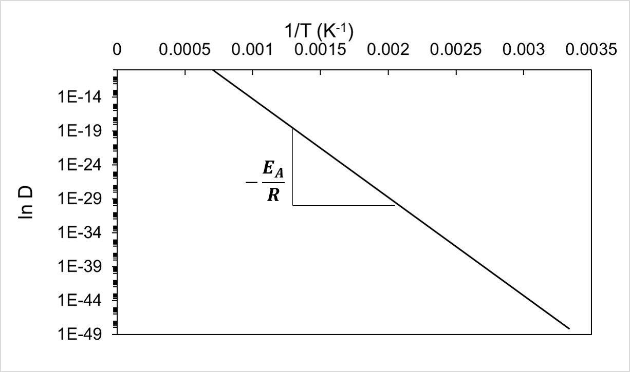
Figure 3: General logarithmic plot of \( D \) vs \( 1/T \) [1]
Due to the Gibbs-Thomson effect, the prevalence of surface melting, higher diffusion coefficient, and low sintering temperature of NPs, the minimum processing temperature of NPs is significantly lower than for microparticles. Note that surface melting and solid-state sintering cannot be simultaneously exploited. Once adjacent particles are joined, the melting temperature returns to its bulk value as seen in Figure 1 which contains theoretical and experimental data [9][13][14][4]. Bridges et al. demonstrated the enhanced diffusivity in nickel NMs as it pertains to brazing Inconel 718 and fitted the diffusion coefficient to a modified version of Hart's equation [15].
\( D_{eff} = \beta D_{Surface}+(1-\beta)(\frac{3\delta}{d}D_{GB}+(1-\frac{3\delta}{d})D_{Lattice}) \) (12)
\( \beta=LhS \) (13)
\( D_{eff} \) is the effective diffusion coefficient and β is a prefactor added to account for the percentage of the atoms that participate in surface diffusion. \( L \) is the number of atomic layers that participate in surface diffusion (assumed to be 3 in Bridges et al.). \( h \) is the atomic diameter and \( S \) is the particle SAV ratio. The normal Hart's equation only considers lattice and grain boundary diffusion, but due to the high surface area to volume ratio of NMs surface diffusion should also be considered. While this version of Hart's equation proved highly effective at predicting the diffusion coefficient of Ni NPs, it was not as effective at predicting the diffusion coefficient of Ni NWs as seen in Figure 4.
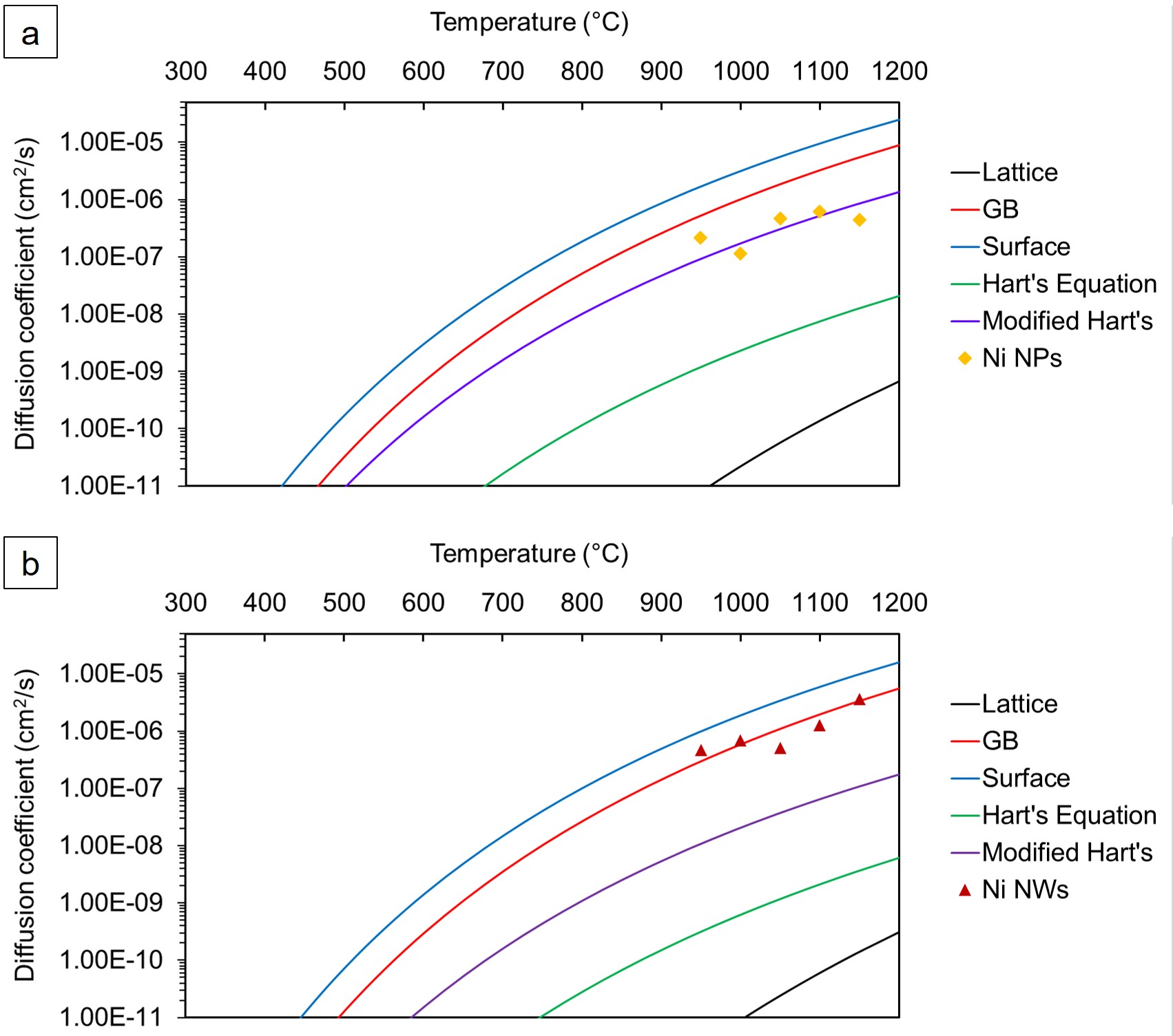
Figure 4: Ni interdiffusion coefficients as a function of temperature at a heating rate of 15 °C for (a) Ni NPs and (b) Ni NWs [15].
2. Low-temperature Nanojoining
Low-temperature nanojoining typically occurs in the soldering temperature regime (< 450 °C) and utilizes either solid-state sintering or surface melting phenomena, but usually not complete melting of the nanomaterials. Being able to utilize the low processing temperature of NMs, damage to electronic components or polymeric substrates can be avoided. Cu-based and Ag-based NPs and NWs are among the most popular choices for soldering and electronic applications due to their high conductivity. For example, Li et al. have used silver nanoplates and nanowires to fabricate flexible electronics and for wire bonding applications [16][17][18]. To avoid damaging temperature-sensitive components in a SiC power electronic device, Manikam et al. mixed aluminum and silver nanoparticles for die attach applications and demonstrated its robustness under thermo-cycling conditions [19]. Nanowire-nanowire joining (Figure 4) is useful for different sensing applications such as sensing and flexible electronic applications since nanowire electronics have better flexibility than nanoparticle electronics [16]. Also, single nanowire devices have applications in high sensitivity detectors [20]. The bonding strength for low-temperature nanojoining is typically limited to tens of MPa [21]. Additionally, low-temperature nanojoining typically suffers from high porosity joints at the end of the heating cycle due to the presence of an organic shell on chemically synthesized NPs and/or from the organic vehicle in the paste. Organic content prevents intimate contact between adjacent NPs and hinders joining mechanisms as demonstrated in [22][23]. Carbon can possibly reduce the melting temperature of some metallic NPs after decomposition of the organic layer, but presumably, this is contingent on the dissolution of carbon into the NP surface and interior.
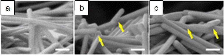
Figure 4: This figure is modified from Li et al. [16]. Ag NWs (a) before sintering, after (b) photonic sintering (ambient temperature is room temperature), and (x) thermal sintering at 250 °C for 5 min. The white scale bars indicate 150 nm and the yellow arrows indicate places where NW-NW joining has occurred [1]
Photonic sintering allows for certain NMs to be joined as low as room temperature (ambient) with a series of high-intensity camera flashes or a pulsed laser [24] which proves useful for manufacturing printable electronics.
3. High-temperature Nanojoining
High-temperature nanojoining typically occurs in the brazing temperature regime (> 450 °C). Brazing involves the melting and reflow of molten filler metal into a gap between joined surfaces. Unlike welding, the base material is not melted during brazing, but sometimes a reaction occurs between the base material and the filler metal. Keeping the base material in a solid-state is highly advantageous for joining materials that experience unfavorable phase transformations during welding and/or repairing components with complex geometries without destroying the component. For example, this is an important procedure for repairing service cracks in turbine blades that utilize special high-temperature alloys [23][25][26]. In order to ensure that the melting temperature of the filler metal is significantly lower than the base material, traditional brazing materials sometimes contain melting point depressants such as boron and silicon, especially those designed for high-temperature alloys such as nickel superalloys. These melting point depressants diffuse into the base material upon brazing and the resulting joint has a higher melting temperature since it has a lower final concentration of melting point depressants. As a consequence, some of the commonly used melting point depressants produce brittle intermetallic compounds in the base material which negatively impact the properties. As a filler metal, NMs have been explored significantly less for brazing than they have for soldering and printable electronics. Due to the size-dependent melting point depression in NMs, it holds a distinct advantage over traditional nanomaterials by not requiring melting point depressants [1]. The size-dependent melting point depression allows for at least a couple of different possibilities:
1) The use of filler metals that would otherwise not be useable with certain base metals such as pure nickel (TmB = 1455 °C) being used to braze Inconel 718 (Melting range = 1370-1430 °C) [15][27].
2) Joining of base metals at temperatures far below the melting point of the commercial equivalent brazing alloy. For example, using copper-silver nanopastes the minimum joining temperature for Inconel 718 reduced from 779.1 °C to as low as 300 °C [28][29] as compared to BAg-8 alloy.
In both scenarios, the NM filler metal will not remelt at the particle melting temperature, but at the bulk melting temperature and, if particle-particle joining is sufficient, will not undergo other phenomena such as surface melting at particle surface melting temperatures [1]. Additionally, in some cases, NM-based filler metals are capable of outperforming their traditional brazing alloy counterpart [28][15][27].
References
- Bridges, Denzel, "Nanobrazing of Inconel 718 and Ti-6Al-4V. " PhD diss., University of Tennessee, 2019.https://trace.tennessee.edu/utk_graddiss/5600
- Huo, S.; Qian, M.; Schaffer, G. & Crossin, E.. Fundamentals of Aluminium Metallurgy; Lumley, R. , Eds.; Woodhead Publishing: Oxford, 2011; pp. 655 - 701.
- R. Lipowsky; Critical Surface Phenomena at First-Order Bulk Transitions. Physical Review Letters 1982, 49, 1575-1578, 10.1103/physrevlett.49.1575.
- Ph. Buffat; J-P. Borel; Size effect on the melting temperature of gold particles. Physical Review A 1976, 13, 2287-2298, 10.1103/physreva.13.2287.
- Lasse Makkonen; On the Methods To Determine Surface Energies. Langmuir 2000, 16, 7669-7672, 10.1021/la990815p.
- Donald H. Andrews; The Collected Works of J. Willard Gibbs. Two volumes. Journal of Chemical Education 1929, 6, 291, 10.1021/ed006p591.2.
- W.H. Qi; M.P. Wang; Size and shape dependent melting temperature of metallic nanoparticles. Materials Chemistry and Physics 2004, 88, 280-284, 10.1016/j.matchemphys.2004.04.026.
- A.P. Chernyshev; Effect of nanoparticle size on the onset temperature of surface melting. Materials Letters 2009, 63, 1525-1527, 10.1016/j.matlet.2009.04.009.
- German, R. Sintering Theory and Practice. John Wiley & Sons, Inc., New York, NY, (1996).
- Bridges, D., Li, R., Gao, Z., Wang, Z., Wang, Z., Hu, A., and Feng, Z. Metallic Nanopastes for Power Electronic Packaging, book section 10. Taylor & Francis Group, Boca Raton, Florida (2017).
- Zhigang Zak Fang; Hongtao Wang; Vineet Kumar; Coarsening, densification, and grain growth during sintering of nano-sized powders—A perspective. International Journal of Refractory Metals and Hard Materials 2016, 62, 110-117, 10.1016/j.ijrmhm.2016.09.004.
- Q. Jiang; S.H. Zhang; J.C. Li; Grain size-dependent diffusion activation energy in nanomaterials. Solid State Communications 2004, 130, 581-584, 10.1016/j.ssc.2004.03.033.
- Z. Z. Fang; H. Wang; Densification and grain growth during sintering of nanosized particles. International Materials Reviews 2008, 53, 326-352, 10.1179/174328008x353538.
- Mehdi Rahimian; Naser Ehsani; Nader Parvin; Hamid Reza Baharvandi; The effect of particle size, sintering temperature and sintering time on the properties of Al–Al2O3 composites, made by powder metallurgy. Journal of Materials Processing Technology 2009, 209, 5387-5393, 10.1016/j.jmatprotec.2009.04.007.
- Denzel Bridges; Ben Nielsen; Lingyue Zhang; Suhong Zhang; Raymond Xu; Anming Hu; Wettability, Diffusion Behaviors, and Modeling of Ni Nanoparticles and Nanowires in Brazing Inconel 718. Advanced Engineering Materials 2020, 23, 2001053, 10.1002/adem.202001053.
- Ruo-Zhou Li; Anming Hu; Tong Zhang; Ken D. Oakes; Direct Writing on Paper of Foldable Capacitive Touch Pads with Silver Nanowire Inks. ACS Applied Materials & Interfaces 2014, 6, 21721-21729, 10.1021/am506987w.
- Ruo-Zhou Li; Tong Zhang; Anming Hu; Denzel Bridges; Ag Nanowire and Nanoplate Composite Paste for Low Temperature Bonding. MATERIALS TRANSACTIONS 2014, 56, 984-987, 10.2320/matertrans.mi201414.
- Ruo-Zhou Li; Anming Hu; Denzel Bridges; Tong Zhang; Ken D. Oakes; Rui Peng; Uma Tumuluri; Zili Wu; Zhili Feng; Robust Ag nanoplate ink for flexible electronics packaging. Nanoscale 2014, 7, 7368-7377, 10.1039/c5nr00312a.
- Vemal Raja Manikam; Khairunisak Abdul Razak; Kuan Yew Cheong; Reliability of sintered Ag80–Al20 die attach nanopaste for high temperature applications on SiC power devices. Microelectronics Reliability 2013, 53, 473-480, 10.1016/j.microrel.2012.10.007.
- Yangbao Deng; Yanfeng Bai; Yongchao Yu; Shuguang Deng; Ye Tian; Guangfu Zhang; Chong Zheng; Jayne Wu; Anming Hu; Laser nanojoining of copper nanowires. Journal of Laser Applications 2019, 31, 022414, 10.2351/1.5096137.
- Peng Peng; Anming Hu; Adrian P. Gerlich; Guisheng Zou; Litian Liu; Y. Norman Zhou; Joining of Silver Nanomaterials at Low Temperatures: Processes, Properties, and Applications. ACS Applied Materials & Interfaces 2015, 7, 12597-12618, 10.1021/acsami.5b02134.
- Shuai Wang; Mingyu Li; Hongjun Ji; Chunqing Wang; Rapid pressureless low-temperature sintering of Ag nanoparticles for high-power density electronic packaging. Scripta Materialia 2013, 69, 789-792, 10.1016/j.scriptamat.2013.08.031.
- Charles, A. and Taylor, C. Development of a Method to Repair Gas Turbine Blades using Electron Beam Melting Additive Manufacturing Technology. Thesis, KTH Royal Institute of Technology, (2016).
- A. Hu; R. Li; D. Bridges; W. Zhou; S. Bai; D. Ma; P. Peng; Photonic nanomanufacturing of high performance energy devices on flexible substrates. Journal of Laser Applications 2016, 28, 022602, 10.2351/1.4944449.
- Hawk, C. WIDE GAP BRAZE REPAIRS OF NICKEL SUPERALLOY GAS TURBINE COMPONENTS. Thesis, (2016).
- Xiao Huang; Warren Miglietti; Wide Gap Braze Repair of Gas Turbine Blades and Vanes—A Review. Journal of Engineering for Gas Turbines and Power 2011, 134, 010801, 10.1115/1.4003962.
- Denzel Bridges; Raymond Xu; Anming Hu; Microstructure and mechanical properties of Ni nanoparticle-bonded Inconel 718. Materials & Design 2019, 174, 107784, 10.1016/j.matdes.2019.107784.
- Denzel Bridges; Chaoli Ma; Zane Palmer; Shutong Wang; Zhili Feng; Anming Hu; Laser brazing of Inconel® 718 using Ag and Cu-Ag nanopastes as brazing materials. Journal of Materials Processing Technology 2017, 249, 313-324, 10.1016/j.jmatprotec.2017.06.010.
- Chaoli Ma; Songbai Xue; Denzel Bridges; Zane Palmer; Zhili Feng; Anming Hu; Low temperature brazing nickel with Ag nanoparticle and Cu-Ag core-shell nanowire nanopastes. Journal of Alloys and Compounds 2017, 721, 431-439, 10.1016/j.jallcom.2017.06.016.