
| Version | Summary | Created by | Modification | Content Size | Created at | Operation |
|---|---|---|---|---|---|---|
| 1 | Guozhu Zhang | + 1688 word(s) | 1688 | 2021-03-09 09:52:27 | | | |
| 2 | Vicky Zhou | Meta information modification | 1688 | 2021-03-16 10:27:18 | | | | |
| 3 | Vicky Zhou | Meta information modification | 1688 | 2021-03-18 09:45:30 | | |
Video Upload Options
During the past two decades, one–dimensional (1D) metal–oxide nanowire (NW)-based molecular sensors have been witnessed as promising candidates to electrically detect volatile organic compounds (VOCs) due to their high surface to volume ratio, single crystallinity, and well-defined crystal orientations. Furthermore, these unique physical/chemical features allow the integrated sensor electronics to work with a long-term stability, ultra-low power consumption, and miniature device size, which promote the fast development of “trillion sensor electronics” for Internet of things (IoT) applications.
1. Introduction
For the upcoming “trillion sensor electronics” era, molecular sensor and electronic recognition devices, which collect the enormous chemical information as big data from various volatile organic molecules (VOCs), are gaining increasing interests in health care[1][2][3], environment[1][4][5], security[6][7][8][9] and agriculture areas[3][4][10][11]. Among various molecular sensors, chemiresistive sensors integrated with metal–oxide semiconductor (MOS) nanostructures are of particular interest due to their high sensitivity and fast response[12][13][14][15][16]. Especially with the advancement of nanomaterial fabrication technology, a large number of functional MOS nanostructures, such as nanodots[17][18], nanowires[19][20][21][22], nanosheets[23][24][25], and hierarchical nanostructures[26][27][28], are synthesized as building blocks for the fabrication of sensor electronics.
Among these nanostructured forms, 1D MOS nanowires offer an ideal platform for nanoscale sensor integration due to their high surface to volume ratio, comparable sized Debye length, high crystallinity, excellent surface chemical reaction, and low power consumption[29][30][31]. Ever since the first report of using the 1D metal–oxide nanostructure as the gas sensor by Comini, great progress has been achieved in the past two decades[32]. To date, hundreds of papers have been published on molecular sensors integration based on 1D metal–oxide nanostructures (SnO2[29], In2O3[33], Fe2O3[34], V2O5[35], CeO2[36], ZnO[37], WO3[38], NiO[39], CuO[40], NaNbO3[41], Zn2SnO4[42][43], CdIn2O4[44], etc.), and the numbers of publications related to nanowires and metal–oxide nanowire sensors can be seen in Figure 1. Meanwhile, to fulfill multiple demands of molecule detection and monitoring, nanowire-based sensor devices with different structures, such as flat[45], suspended[46], bridging[47], and vertical structure[48], have also been addressed. Despite much effort being devoted to advancing the metal–oxide nanowire-based molecular sensor electronics, molecular sensors based on 1D MOS nanowires have not yet been successfully commercialized compared to the MOS film structures.
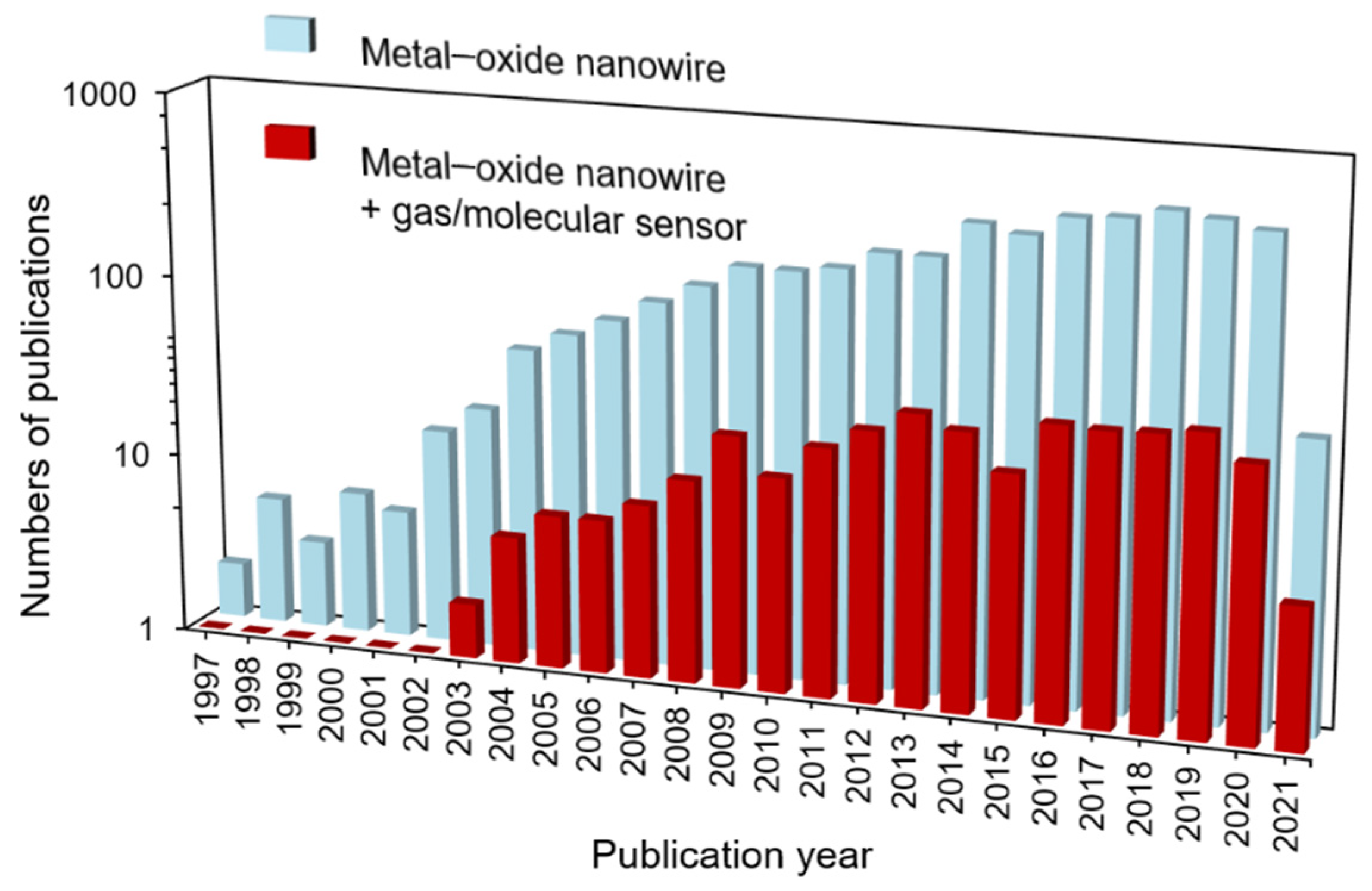
The inherent limitations for the practical applications of the 1D MOS nanowire-based molecular sensors can be summarized as follows:
(1) Lack of effective method for the large-scale synthesis of geometrically uniform single-crystalline nanowires—as is known, the electrical[49], optical[50], thermal[51], and chemical[52] properties of nanomaterials are strongly affected by their size and shape due to the quantum confinement effect[53]. The electrical conduction becomes more sensitive to the field-effect as the nanowire diameter decreases[54]. Until now, although highly crystalline MOS nanowire with various diameters[55], compositions[28][29][30][31][32][33][34][35][36][37][38][39][40] and heterostructures[56][57] can be grown in vapor phase (physical vapor deposition (PVD)[58][59], pulsed laser ablation deposition (PLD)[60][61] and chemical vapor deposition (CVD)[62][63], etc.) and solution phase (hydrothermal[64][65] and solvothermal[66][67]), the large-scale synthesis of geometry uniform (diameter) nanowires is still a big challenge[68].
(2) Poor reproducibility—it has been demonstrated that the nanowires present a fantastic performance as they are integrated into single nanowire devices[69] [69]. For such a kind of device, lithography and sputtering techniques are frequently utilized to design and deposit interdigitated electrodes on randomly distributed nanowires for the device fabrication[70]. However, this process is only accessible for fundamental laboratory research, and assembling scalable and controllable nanowires on arbitrary substrates remains a major challenge toward performance reproducible sensor device fabrication[71].
(3) Poor environmental/thermal stability—to deeply exploit the data science from the obtained sensor signal, the long-term stability of the sensor response is highly required for time-series data collection[72]. However, performance degradation usually occurs in the nanowire-based sensor electronics because the surrounding oxygen, water, and contaminates would react with the active nanowire surface as well as the nanowire–electrode contact when the sensors are exposed to ambient air for molecular detection[47][73][74].
(4) Poor sensor selectivity—although the sensitivity of the single nanowire sensor devices has been demonstrated to possess an exponential enhancement as compared with those thin-film devices[75][76], it is still desired to significantly improve the selectivity of nanowire-based sensor electronics. Therefore, further efforts are still encouraged to promote MOS nanowire-based sensor electronics for the IoT applications.
2. Prospective towards Metal–Oxide Nanowire Gas Sensor Electronics
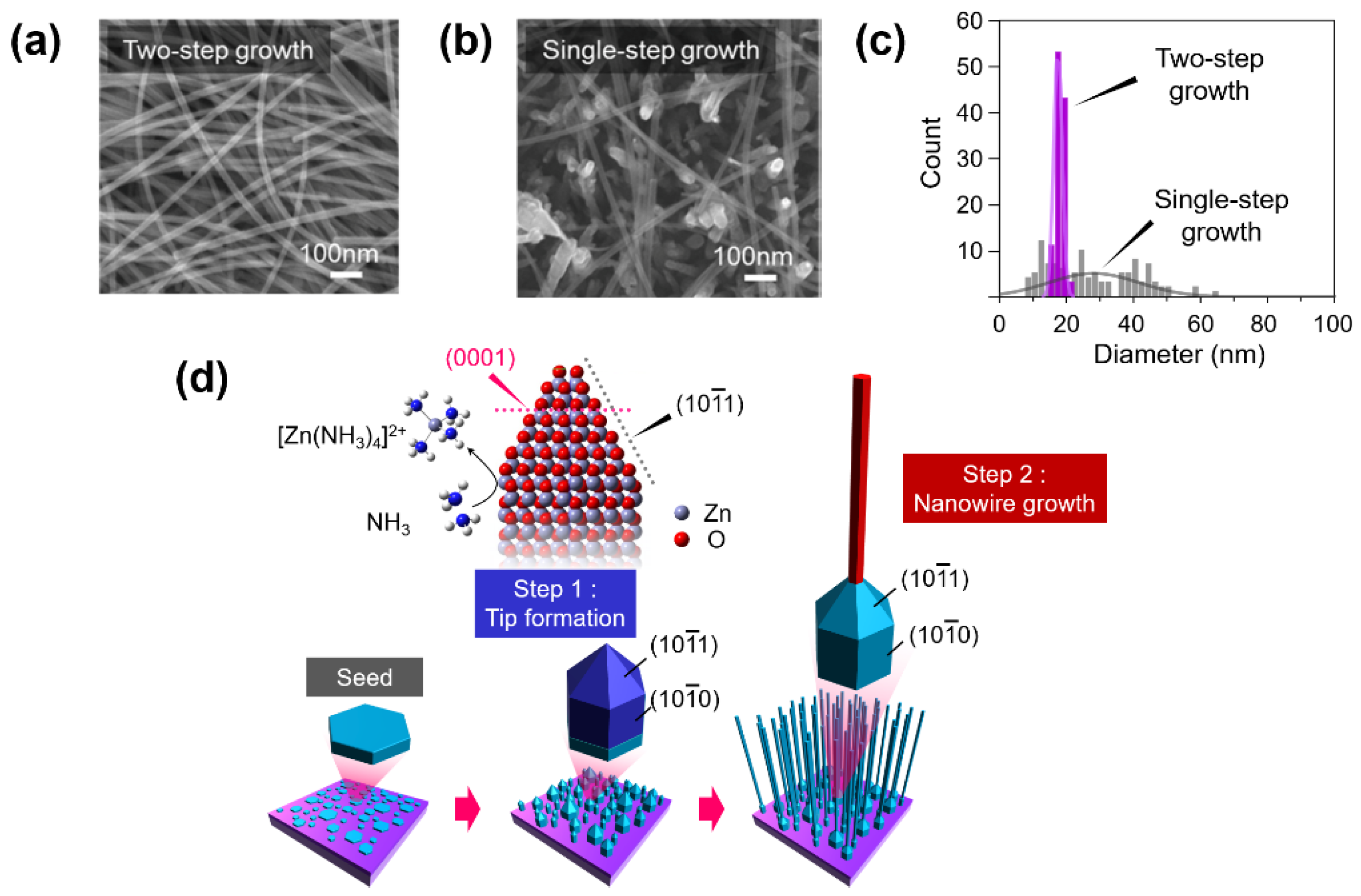
As for the reproducibility of nanowire devices, we should carefully consider how to synthesize nanowires with high uniformity. Template-assisted nanowire growth is considered an alternative approach to achieve a highly ordered nanowire array. However, the complexity of template fabrication, low density of nanowires, and the extensive distribution of nanowire diameter have limited the wide application of such method[77]. Recently, Zhao et al. reported a two-step method to fabricate ZnO nanowires with uniformly shaped structures, as shown in Figure 2[78]. Firstly, ZnO nanowires of random size are etched by NH4+ as the seed layer, and then, a very similar diameter (average about 17 nm with σ 1.3 nm, shown in Figure 2c) of ZnO nanowires are grown in the second step, which significantly increases the reproducibility of metal–oxide nanowire. This unique finding paves the way for the fabrication of nanowires-integrated nanodevices with reliable performance.
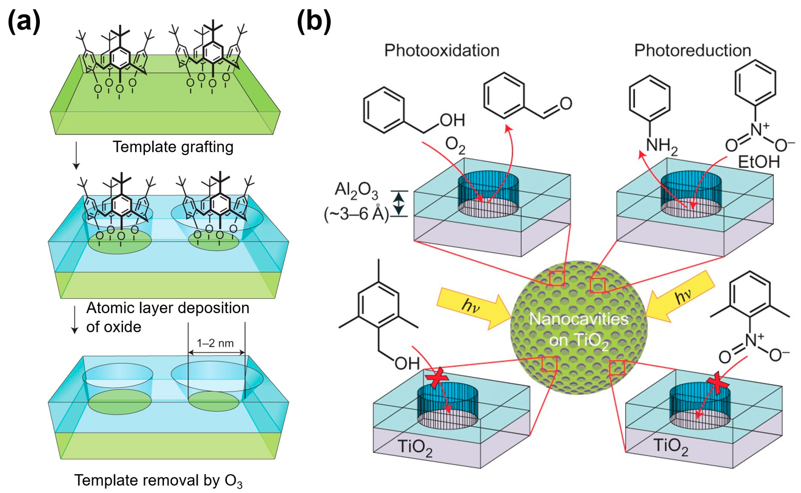
Poor selectivity is a perpetually perplexing problem that limits the wide application of the MOS gas sensor, including the metal–oxide nanowire-based sensors. Inspired by the catalytical chemistry, it is worth considering combining porous materials such as zeolites, metal–organic frameworks, and mesostructured oxides with a metal–oxide nanowire[79][80][81]. Canlas et al. reported a novel method to fabricate molecules imprinted oxide catalyst, and the fabrication process is shown in Figure 3 [82]. Using this structure, the nanocavities can preferentially react with nitrobenzene rather than nitroxylene in the photoreduction model and react with benzyl alcohol rather than 2,4,6-trimethylbenzyl alcohol in the photo-oxidation model. This technique can be applied to the metal–oxide nanowire sensor to gigantically improve selectivity due to their preferential interactions with specific VOC molecules, even with a chemically similar structure.
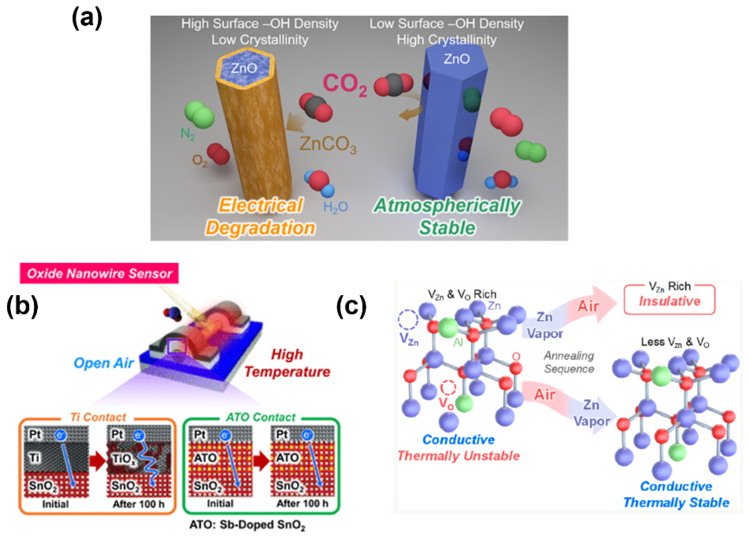
Solving the degradation issues, including nanowire degradation, contact degradation, and electrode degradation, is the only way to achieve long-term stability in nanowire devices. As shown in Figure 4a, Nakamura et al. demonstrated a strategy for achieving the atmospheric electrical stability of ZnO nanowires[74]. Via using a thermal annealing treatment in vacuum/air, the insulating layer induced by the unstable –OH layer on as fabricated ZnO nanowire surface is efficiently eliminated. Such a simple and low-cost method can enhance nanowire atmospheric stability for at least 40 days with stable electrical properties. Meanwhile, Zeng et al. offered a way to overcome the degradation in conventional sensor contact, as shown in Figure 4b [73]. It is found that the nanowire device can obtain good stability for at least over 2000 hours by replacing the easily oxidized contact metal (Ti) with heavily doped metal–oxide (antimony doped tin oxide). Moreover, Yan et al. reported an unusual annealing process on oxide thin films for highly thermal and chemical stability shown in Figure 4c [83][84]. It was indicated that Al-doped ZnO (AZO) nano-thin films could efficiently suppress the inevitable crystal defect formation in the as-fabricated thin film via sequential annealing process under air and Zn vapor atmosphere, resulting in a stable electrical resistivity (~10−4 Ω·cm) in air, even at high temperature (up to 500 °C). This thermally stable thin film can be utilized as electrodes for gas sensors, which obtain stable performance over 250 hours compared to the conventional Ti/Pt contact sensor. Meanwhile, the sequential annealed AZO nano-thin films also show highly chemical stability in buffer solution (pH: 3~11) compared with non-annealed AZO nano-thin films and ZnO thin films. These proposed strategies can successfully suppress the electrical performance degradation of the nanowire devices and have a great potential to be applied to various oxide nanostructures, which would give a foundation for the designing and fabrication of oxide nanomaterial-based IoT sensors with long-term stability.
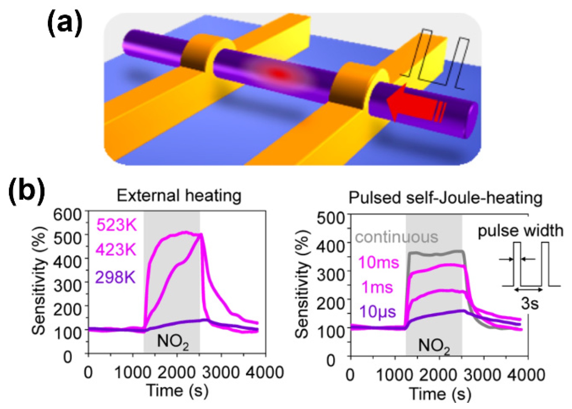
With regard to the low power consumption, Meng et al. recently reported an excellent thermal management approach in metal–oxide nanowire sensors via a pulsed self-Joule-heating technique, as shown in Figure 5 [85]. It was found that the thermal conductivity of the device was reduced due to the prohibition of heat dissipation from nanowire to surroundings, and its thermal relaxation times can be decreased down to a microsecond range, while several tens of seconds are needed for conventional MEMS gas sensors. This method enables the reduction in energy consumption down to ∼102 pJ/s and the enhancement of sensitivity for electrical sensing of NO2 (100 ppb). This proposed thermal management concept of nanowires in both spatial and time domains offers a strategy for exploring novel functionalities of nanowire-based sensors with high performance.
With the improvement of the metal–oxide nanowire synthesis and device fabrication processes with high uniformity, the integrated nanowire sensor electronics would have a high reproducibility, selectivity, and long-term stability. This would promote the nanowire sensor electronics to be widely used in the IoT applications, such as medicine, food industry, security, and environment protection.
References
- Lim, H.; Kim, H.S.; Qazi, R.; Kwon, Y.; Jeong, J.; Yeo, W. Wearable Flexible Hybrid Electronics: Advanced Soft Materials, Sen-sor Integrations, and Applications of Wearable Flexible Hybrid Electronics in Healthcare, Energy, and Environment. Adv. Mater. 2020, 32, 1–43.
- Güntner, A.T.; Abegg, S.; Königstein, K.; Gerber, P.A.; Schmidt-Trucksäss, A.; Pratsinis, S.E. Breath Sensors for Health Moni-toring. ACS Sensors 2019, 4, 268–280.
- Wang, T.; Ramnarayanan, A.; Cheng, H. Real Time Analysis of Bioanalytes in Healthcare, Food, Zoology and Botany. Sensors 2017, 18, 5.
- Dincer, C.; Bruch, R.; Costa‐Rama, E.; Fernández‐Abedul, M.T.; Merkoçi, A.; Manz, A.; Urban, G.A.; Güder, F. Disposable Sensors in Diagnostics, Food, and Environmental Monitoring. Adv. Mater. 2019, 31, 1806739.
- Fang, X.; Zong, B.; Mao, S. Metal–Organic Framework-Based Sensors for Environmental Contaminant Sensing. Nano-Micro Lett. 2018, 10, 1–19.
- Wang, D.; Chen, A.; Jen, A.K.-Y. Reducing cross-sensitivity of TiO2-(B) nanowires to humidity using ultraviolet illumination for trace explosive detection. Phys. Chem. Chem. Phys. 2013, 15, 5017–5021.
- Cao, A.; Zhu, W.; Shang, J.; Klootwijk, J.H.; Sudhölter, E.J.R.; Huskens, J.; De Smet, L.C.P.M. Metal–Organic Polyhedra-Coated Si Nanowires for the Sensitive Detection of Trace Explosives. Nano Lett. 2016, 17, 1–7
- Engel, Y.; Elnathan, R.; Pevzner, A.; Davidi, G.; Flaxer, E.; Patolsky, F. Supersensitive Detection of Explosives by Silicon Nanowire Arrays. Angew. Chem. Int. Ed. 2010, 49, 6830–6835.
- Lan, A.; Li, K.; Wu, H.; Olson, D.H.; Emge, T.J.; Ki, W.; Hong, M.; Li, J. A Luminescent Microporous Metal-Organic Frame-work for the Fast And reversible Detection of High Explosives. Angew. Chemie Int. Ed. 2009, 48, 2334–2338.
- Zappa, D. Low-Power Detection of Food Preservatives by a Novel Nanowire-Based Sensor Array. Foods 2019, 8, 226.
- Carmona, E.N.; Sberveglieri, V.; Ponzoni, A.; Galstyan, V.; Zappa, D.; Pulvirenti, A.; Comini, E. Detection of food and skin pathogen microbiota by means of an electronic nose based on metal oxide chemiresistors. Sensors Actuators B: Chem. 2017, 238, 1224–1230.
- Mirzaei, A.; Lee, J.-H.; Majhi, S.M.; Weber, M.; Bechelany, M.; Kim, H.W.; Kim, S.S. Resistive gas sensors based on metal-oxide nanowires. J. Appl. Phys. 2019, 126, 241102.
- Karnati, P.; Akbar, S.; Morris, P.A. Conduction mechanisms in one dimensional core-shell nanostructures for gas sensing: A review. Sensors Actuators B: Chem. 2019, 295, 127–143.
- Korotcenkov, G. Current Trends in Nanomaterials for Metal Oxide-Based Conductometric Gas Sensors: Advantages and Limitations. Part 1: 1D and 2D Nanostructures. Nanomater. 2020, 10, 1392.
- Majhi, S.M.; Mirzaei, A.; WooKimab, H.; Kim, S.S.; Kim, T.W. Recent advances in energy-saving chemiresistive gas sensors: A review. Nano Energy 2021, 79, 105369.
- Joshi, N.; Hayasaka, T.; Liu, Y.; Liu, H.; Oliveira, O.N.; Lin, L. A review on chemiresistive room temperature gas sensors based on metal oxide nanostructures, graphene and 2D transition metal dichalcogenides. Microchim. Acta 2018, 185, 1–16.
- Mounasamy, V.; Mani, G.K.; Madanagurusamy, S. Vanadium oxide nanostructures for chemiresistive gas and vapour sens-ing: A review on state of the art. Microchim. Acta 2020, 187, 1–29.
- Wang, J.; Zhou, Q.; Peng, S.; Xu, L.; Zeng, W. Volatile Organic Compounds Gas Sensors Based on Molybdenum Oxides: A Mini Review. Front. Chem. 2020, 8, 1–7.
- Comini, E. Metal oxides nanowires chemical/gas sensors: Recent advances. Mater. Today Adv. 2020, 7, 100099.
- Wang, Y.; Duan, L.; Deng, Z.; Liao, J. Electrically Transduced Gas Sensors Based on Semiconducting Metal Oxide Nanowires. Sensors 2020, 20, 6781.
- Meng, J.; Li, Z. Schottky-Contacted Nanowire Sensors. Adv. Mater. 2020, 32, 1–16.
- Kaur, N.; Singh, M.; Comini, E. One-Dimensional Nanostructured Oxide Chemoresistive Sensors. Langmuir 2020, 36, 6326–6344.
- Choi, P.G.; Izu, N.; Shirahata, N.; Masuda, Y. SnO2 Nanosheets for Selective Alkene Gas Sensing. ACS Appl. Nano Mater. 2019, 2, 1820–1827.
- Miao, J.; Chen, C.; Meng, L.; Lin, J.Y. Self-Assembled Monolayer of Metal Oxide Nanosheet and Structure and Gas-Sensing Property Relationship. ACS Sensors 2019, 4, 1279–1290.
- Kim, K.; Choi, P.G.; Itoh, T.; Masuda, Y. Catalyst-free Highly Sensitive SnO2 Nanosheet Gas Sensors for Parts per Billion-Level Detection of Acetone. ACS Appl. Mater. Interfaces 2020, 12, 51637–51644.
- Govindhan, M.; Sidhureddy, B.; Chen, A. High-Temperature Hydrogen Gas Sensor Based on Three-Dimensional Hierar-chical-Nanostructured Nickel–Cobalt Oxide. ACS Appl. Nano Mater. 2018, 1, 6005–6014.
- Zhang, H.; Chen, W.-G.; Li, Y.-Q.; Song, Z.-H. Gas Sensing Performances of ZnO Hierarchical Structures for Detecting Dis-solved Gases in Transformer Oil: A Mini Review. Front. Chem. 2018, 6, 1–7.
- Li, N.; Fan, Y.; Shi, Y.; Xiang, Q.; Wang, X.; Xu, J. A low temperature formaldehyde gas sensor based on hierarchical SnO/SnO2 nano-flowers assembled from ultrathin nanosheets: Synthesis, sensing performance and mechanism. Sensors Actuators B: Chem. 2019, 294, 106–115.
- Kolmakov, A.; Zhang, Y.; Cheng, G.; Moskovits, M. Detection of CO and O2 Using Tin Oxide Nanowire Sensors. Adv. Mater. 2003, 15, 997–1000.
- Huang, M.H.; Mao, S.; Feick, H.; Yan, H.Q.; Wu, Y.Y.; Kind, H.; Weber, E.; Russo, R.; Yang, P.D. Room-Temperature Ultravio-let Nanowire Nanolasers. Science 2001, 292, 1897–1899.
- Li, J.Y.; Qiao, Z.Y.; Chen, X.L.; Chen, L.; Cao, Y.G.; He, M.; Li, H.; Cao, Z.M.; Zhang, Z. Synthesis of β-Ga2O3 Nanorods. J. Al-loys Compd. 2000, 306, 300–302.
- Comini, E.; Faglia, G.; Sberveglieri, G.; Pan, Z.; Wang, Z.L. Stable and highly sensitive gas sensors based on semiconducting oxide nanobelts. Appl. Phys. Lett. 2002, 81, 1869–1871.
- Vomiero, A.; Bianchi, S.; Comini, E.; Faglia, G.; Ferroni, M.; Sberveglieri, G. Controlled Growth and Sensing Properties of In2O3 Nanowires. Cryst. Growth Des. 2007, 7, 2500–2504.
- Lupan, O.; Postica, V.; Wolff, N.; Polonskyi, O.; Duppel, V.; Kaidas, V.; Lazari, E.; Ababii, N.; Faupel, F.; Kienle, L.; et al. Lo-calized Synthesis of Iron Oxide Nanowires and Fabrication of High Performance Nanosensors Based on a Single Fe2O3 Nan-owire. Small 2017, 13, 1–10.
- Jin, W.; Yan, S.; An, L.; Chen, W.; Yang, S.; Zhao, C.; Dai, Y. Enhancement of ethanol gas sensing response based on ordered V2O5 nanowire microyarns. Sens. Actuators B: Chem. 2015, 206, 284–290.
- Fu, X.Q.; Wang, C.; Yu, H.C.; Wang, Y.G.; Wang, T.H. Fast humidity sensors based on CeO2 nanowires. Nanotechnology 2007, 18, 145503.
- Baratto, C.; Kumar, R.; Comini, E.; Faglia, G.; Sberveglieri, G. Gas Sensing Study of ZnO Nanowire Heterostructured with NiO for Detection of Pollutant Gases. Procedia Eng. 2014, 87, 1091–1094.
- Kaur, N.; Zappa, D.; Poli, N.; Comini, E. Integration of VLS-Grown WO3 Nanowires into Sensing Devices for the Detection of H2S and O3. ACS Omega 2019, 4, 16336–16343.
- Kaur, N.; Comini, E.; Zappa, D.; Poli, N.; Sberveglieri, G. Nickel oxide nanowires: Vapor liquid solid synthesis and integration into a gas sensing device. Nanotechnology 2016, 27, 205701.
- Lupan, O.; Cretu, V.; Postica, V.; Ahmadi, M.; Cuenya, B.R.; Chow, L.; Tiginyanu, I.; Viana, B.; Pauporté, T.; Adelung, R. Sil-ver-Doped Zinc Oxide Single Nanowire Multifunctional Nanosensor with a Significant Enhancement in Response. Sens. Actu-ators B Chem. 2016, 223, 893–903.
- Gu, L.; Zhou, D.; Cao, J.C. Piezoelectric Active Humidity Sensors Based on Lead-Free NaNbO3 Piezoelectric Nanofibers. Sen-sors 2016, 16, 833.
- Zhou, T.; Liu, X.; Zhang, R.; Wang, Y.; Zhang, T. Shape control and selective decoration of Zn2SnO4 nanostructures on 1D nanowires: Boosting chemical–sensing performances. Sensors Actuators B: Chem. 2019, 290, 210–216.
- Thanh, H.X.; Trung, D.D.; Trung, K.Q.; Van Dam, K.; Van Duy, N.; Hung, C.M.; Hoa, N.D.; Van Hieu, N. On-chip growth of single phase Zn2SnO4 nanowires by thermal evaporation method for gas sensor application. J. Alloy. Compd. 2017, 708, 470–475.
- Cheng, Z.; Huang, C.; Song, L.; Wang, Y.; Ding, Y.; Xu, J.; Zhang, Y. Electrospinning synthesis of CdIn2O4 nanofibers for etha-nol detection. Sens. Actuators B: Chem. 2015, 209, 530–535.
- Gu, G.; Zheng, B.; Han, W.Q.; Roth, S.; Liu, J. Tungsten Oxide Nanowires on Tungsten Substrates. Nano Lett. 2002, 2, 849–851.
- Baek, D.-H.; Choi, J.; Kim, J. Fabrication of suspended nanowires for highly sensitive gas sensing. Sensors Actuators B: Chem. 2019, 284, 362–368.
- Steinhauer, S.; Chapelle, A.; Menini, P.; Sowwan, M. Local CuO Nanowire Growth on Microhotplates: In Situ Electrical Meas-urements and Gas Sensing Application. ACS Sensors 2016, 1, 503–507.
- Chen, J.; Wang, K.; Zhou, W. Vertically Aligned ZnO Nanorod Arrays Coated with SnO2/Noble Metal Nanoparticles for Highly Sensitive and Selective Gas Detection. IEEE Trans. Nanotechnol. 2010, 10, 968–974.
- Ford, A.C.; Ho, J.C.; Chueh, Y.-L.; Tseng, Y.-C.; Fan, Z.; Guo, J.; Bokor, J.; Javey, A. Diameter-Dependent Electron Mobility of InAs Nanowires. Nano Lett. 2009, 9, 360–365.
- Duan, J.-L.; Liu, J.; Yao, H.-J.; Mo, D.; Hou, M.-D.; Sun, Y.-M.; Chen, Y.-F.; Zhang, L. Controlled synthesis and diame-ter-dependent optical properties of Cu nanowire arrays. Mater. Sci. Eng. B 2008, 147, 57–62.
- Li, D.; Wu, Y.; Kim, P.; Shi, L.; Yang, P.; Majumdar, A. Thermal conductivity of individual silicon nanowires. Appl. Phys. Lett. 2003, 83, 2934–2936.
- Tonezzer, M.; Hieu, N. Size-dependent response of single-nanowire gas sensors. Sens. Actuators B: Chem. 2012, 163, 146–152.
- Xia, Y.; Yang, P.; Sun, Y.; Wu, Y.; Mayers, B.; Gates, B.; Yin, Y.; Kim, F.; Yan, H. One-Dimensional Nanostructures: Synthesis, Characterization, and Applications. Adv. Mater. 2003, 15, 353–389.
- Gröttrup, J.; Postica, V.; Ababii, N.; Lupan, O.; Zamponi, C.; Meyners, D.; Mishra, Y.K.; Sontea, V.; Tiginyanu, I.; Adelung, R. Size-Dependent UV and Gas Sensing Response of Individual Fe2O3-ZnO:Fe Micro- and Nanowire Based Devices. J. Alloys Compd. 2017, 701, 920–925.
- Kim, K.; Kwak, H.-T.; Cho, H.; Meyyappan, M.; Baek, C.-K. Design Guidelines for High Sensitivity ZnO Nanowire Gas Sen-sors with Schottky Contact. IEEE Sensors J. 2019, 19, 976–981.
- Walker, J.M.; Akbar, S.A.; Morris, P.A. Synergistic effects in gas sensing semiconducting oxide nano-heterostructures: A re-view. Sensors Actuators B: Chem. 2019, 286, 624–640.
- Zappa, D.; Galstyan, V.; Kaur, N.; Munasinghe Arachchige, H.M.M.; Sisman, O.; Comini, E. “Metal Oxide -Based Hetero-structures for Gas Sensors”- A Review. Anal. Chim. Acta 2018, 1039, 1–23.
- Simakov, V.; Sinev, I.; Shikunov, D.; Tymoshenko, D.; Smirnov, A.; Zaitsev, B. Experimental investigation and modeling of temperature influence on vertical and radial growth rate of tin dioxide nanowires synthesized by catalyst-free thermal evap-oration method. Mater. Chem. Phys. 2020, 242, 122502.
- Singh, N.; Ponzoni, A.; Comini, E.; Lee, P.S. Chemical sensing investigations on Zn–In2O3 nanowires. Sensors Actuators B: Chem. 2012, 171, 244–248.
- Liu, Z.; Zhang, D.; Han, S.; Li, C.; Tang, T.; Jin, W.; Liu, X.; Lei, B.; Zhou, C. Laser Ablation Synthesis and Electron Transport Studies of Tin Oxide Nanowires. Adv. Mater. 2003, 15, 1754–1757.
- Shkurmanov, A.; Sturm, C.; Franke, H.; Lenzner, J.; Grundmann, M. Low-Temperature PLD-Growth of Ultrathin ZnO Nan-owires by Using ZnxAl1−xO and ZnxGa1−xO Seed Layers. Nanoscale Res. Lett. 2017, 12, 1–7.
- Liang, J.; Zhao, Y.; Zhu, K.; Guo, J.; Zhou, L. Synthesis and room temperature NO2 gas sensitivity of vanadium dioxide nan-owire structures by chemical vapor deposition. Thin Solid Films 2019, 669, 537–543.
- Vallejos, S.; Gràcia, I.; Lednický, T.; Vojkuvka, L.; Figueras, E.; Hubálek, J.; Cané, C. Highly Hydrogen Sensitive Microm-achined Sensors Based on Aerosol-Assisted Chemical Vapor Deposited ZnO Rods. Sens. Actuators B Chem. 2018, 268, 15–21.
- Nekita, S.; Nagashima, K.; Zhang, G.; Wang, Q.; Kanai, M.; Takahashi, T.; Hosomi, T.; Nakamura, K.; Okuyama, T.; Yanagida, T. Face-Selective Crystal Growth of Hydrothermal Tungsten Oxide Nanowires for Sensing Volatile Molecules. ACS Appl. Nano Mater. 2020, 3, 10252–10260.
- Liu, Q.; Yasui, T.; Nagashima, K.; Yanagida, T.; Hara, M.; Horiuchi, M.; Zhu, Z.; Takahashi, H.; Shimada, T.; Arima, A.; et al. Ammonia-Induced Seed Layer Transformations in a Hydrothermal Growth Process of Zinc Oxide Nanowires. J. Phys. Chem. C 2020, 124, 20563–20568.
- Wang, Q.; Huang, J.; Zhou, J.; Liu, Z.; Geng, Y.; Liang, Z.; Du, Y.; Tian, X. Different nanostructured tungsten oxides synthe-sized by facile solvothermal route for chlorine gas sensing. Sens. Actuators B: Chem. 2018, 275, 306–311
- Qin, Y.; Li, X.; Wang, F.; Hu, M. Solvothermally synthesized tungsten oxide nanowires/nanorods for NO2 gas sensor applica-tions. J. Alloy. Compd. 2011, 509, 8401–8406.
- Dasgupta, N.P.; Sun, J.; Liu, C.; Brittman, S.; Andrews, S.C.; Lim, J.; Gao, H.; Yan, R.; Yang, P. 25th Anniversary Article: Semi-conductor Nanowires-Synthesis, Characterization, and Applications. Adv. Mater. 2014, 26, 2137–2184.
- Asadzadeh, M.Z.; Köck, A.; Popov, M.; Steinhauer, S.; Spitaler, J.; Romaner, L. Response modeling of single SnO2 nanowire gas sensors. Sens. Actuators B: Chem. 2019, 295, 22–29.
- Gall, O.Z.; Zhong, X.; Schulman, D.S.; Kang, M.; Razavieh, A.; Mayer, T.S. Titanium dioxide nanowire sensor array integration on CMOS platform using deterministic assembly. Nanotechnology 2017, 28, 265501.
- Jeong, S.; Kim, J.; Lee, J. Rational Design of Semiconductor‐Based Chemiresistors and their Libraries for Next‐Generation Arti-ficial Olfaction. Adv. Mater. 2020, 32, 1–47.
- Zhou, Z.; Lan, C.; Wei, R.; Ho, J.C. Transparent metal-oxide nanowires and their applications in harsh electronics. J. Mater. Chem. C 2018, 7, 202–217.
- Zeng, H.; Takahashi, T.; Kanai, M.; Zhang, G.; He, Y.; Nagashima, K.; Yanagida, T. Long-Term Stability of Oxide Nanowire Sensors via Heavily Doped Oxide Contact. ACS Sens. 2017, 2, 1854–1859.
- Nakamura, K.; Takahashi, T.; Hosomi, T.; Seki, T.; Kanai, M.; Zhang, G.; Nagashima, K.; Shibata, N.; Yanagida, T. Re-dox-Inactive CO2 Determines Atmospheric Stability of Electrical Properties of ZnO Nanowire Devices through a Room-Temperature Surface Reaction. ACS Appl. Mater. Interfaces 2019, 11, 40260–40266.
- Zhang, D.; Liu, Z.; Li, C.; Tang, T.; Liu, X.; Han, S.; Lei, A.B.; Zhou, C. Detection of NO2 down to ppb Levels Using Individual and Multiple In2O3 Nanowire Devices. Nano Lett. 2004, 4, 1919–1924.
- Verma, V.P.; Das, S.; Hwang, S.; Choi, H.; Jeon, M.; Choi, W. Nitric oxide gas sensing at room temperature by functionalized single zinc oxide nanowire. Mater. Sci. Eng. B 2010, 171, 45–49.
- Subannajui, K.; GüderF.; Zacharias, M. Bringing Order to the World of Nanowire Devices by Phase Shift Lithography. Nano Lett. 2011, 11, 3513–3518.
- Zhao, X.; Nagashima, K.; Zhang, G.; Hosomi, T.; Yoshida, H.; Akihiro, Y.; Kanai, M.; Mizukami, W.; Zhu, Z.; Takahashi, T.; et al. Synthesis of Monodispersedly Sized ZnO Nanowires from Randomly Sized Seeds. Nano Lett. 2019, 20, 599–605.
- Hall, A.S.; Yoon, Y.; Wuttig, A.; Surendranath, Y. Mesostructure-Induced Selectivity in CO2 Reduction Catalysis. J. Am. Chem. Soc. 2015, 137, 14834–14837.
- Liu, J.; Chen, L.; Cui, H.; Zhang, J.; Zhang, L.; Su, C.-Y. Applications of metal–organic frameworks in heterogeneous supra-molecular catalysis. Chem. Soc. Rev. 2014, 43, 6011–6061.
- Nugent, P.; Belmabkhout, Y.; Burd, S.D.; Cairns, A.J.; Luebke, R.; A Forrest, K.; Pham, T.; Ma, S.; Space, B.; Wojtas, L.; et al. Porous materials with optimal adsorption thermodynamics and kinetics for CO2 separation. Nat. Cell Biol. 2013, 495, 80–84.
- Canlas, C.P.; Lu, J.; Ray, N.A.; Grosso-Giordano, N.A.; Lee, S.; Elam, J.W.; Winans, R.E.; Van Duyne, R.P.; Stair, P.C.; Notestein, J.M. Shape-selective sieving layers on an oxide catalyst surface. Nat. Chem. 2012, 4, 1030–1036.
- Yan, R.; Takahashi, T.; Kanai, M.; Hosomi, T.; Zhang, G.; Nagashima, K.; Yanagida, T. Unusual Sequential Annealing Effect in Achieving High Thermal Stability of Conductive Al-Doped ZnO Nanofilms. ACS Appl. Electron. Mater. 2020, 2, 2064–2070.
- Yan, R.; Takahashi, T.; Zeng, H.; Hosomi, T.; Kanai, M.; Zhang, G.; Nagashima, K.; Yanagida, T. Enhancement of PH Tolerance in Conductive Al-Doped ZnO Nanofilms via Sequential Annealing. ACS Appl. Electron. Mater. 2021, DOI: 10.1021/acsaelm.0c01052.
- Meng, G.; Zhuge, F.; Nagashima, K.; Nakao, A.; Kanai, M.; He, Y.; Boudot, M.; Takahashi, T.; Uchida, K.; Yanagida, T. Na-noscale Thermal Management of Single SnO2 Nanowire: Pico-Joule Energy Consumed Molecule Sensor. ACS Sens. 2016, 1, 997–1002.


