 +1 credit
| Version | Summary | Created by | Modification | Content Size | Created at | Operation |
|---|---|---|---|---|---|---|
| 1 | Robert Ambroziak | + 1691 word(s) | 1691 | 2021-01-12 06:46:25 | | | |
| 2 | Vicky Zhou | Meta information modification | 1691 | 2021-02-10 09:57:05 | | | | |
| 3 | Vicky Zhou | Meta information modification | 1691 | 2021-02-10 09:57:47 | | |
Video Upload Options
The efficiency of the generation of Raman spectra by molecules adsorbed on some substrates (or placed at a very close distance to some substrates) may be many orders of magnitude larger than the efficiency of the generation of Raman spectra by molecules that are not adsorbed. This effect is called surface-enhanced Raman scattering (SERS). In the first SERS experiments, nanostructured plasmonic metals have been used as SERS-active materials. Later, other types of SERS-active materials have also been developed.
1. Introduction
Raman scattering relies on an inelastic photon scattering. In contrast to elastic Rayleigh scattering, inelastically scattered photons have different energy from the incident ones. For many years Raman spectroscopy has not been considered a useful analytical tool because of very low efficiency of the “normal” Raman scattering. Typical total Raman scattering cross-section is only ca. 10−29 cm2 per molecule, whereas typical cross-sections for absorption in ultraviolet and infrared are ca. 10−18 and 10−21 cm2 per molecule, respectively[1]. In 1974 Fleischmann et al. reported a significant growth of the Raman signal measured from pyridine adsorbed on electrochemically roughened (nanostructured) silver substrate[2]. They interpreted this effect as a result of an increase of the surface area of electrochemically roughened silver electrode and hence adsorption of a significantly larger number of pyridine molecules. Three years later two independent research groups found true reasons for the very large growth of the intensity of the Raman signal observed by Fleischmann et al.[2] Jeanmaire and van Duyne[3], and Albrecht and Creighton[4] connected very strong Raman signal observed for pyridine adsorbed on nanostructured Ag surface with the increase of the efficiency of Raman scattering. The observed effect was called SERS (surface-enhanced Raman scattering). As mentioned above, the increase of the efficiency of Raman scattering for molecules being in the close proximity to the plasmonic nanoparticles is mainly due to the increase of the intensity of the electromagnetic field
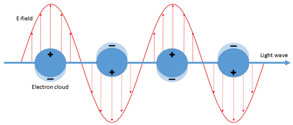
It is generally accepted that the enhancement of SERS spectra is due to the cooperation of two mechanisms: the electromagnetic and the chemical one. The electromagnetic mechanism is due to inducing the SERS substrate by the electromagnetic wave of the electric dipole (see Figure 1), which may lead to a significant local increase in the intensity of the electric field.
The total SERS enhancement is proportional to the fourth power of the local electromagnetic field (Equation 1).

where: E0 - value of the intensity of the electric field of the incident excitation beam (amplified by the interaction with the plasmonic system); Eω - value of the intensity of the electric field of the scattered beam (also amplified by the interaction with the plasmonic system)
In the case of an isolated nanoparticle, the strongest field enhancement usually occurs on its sharp edges[6][7]. In the case of dimers and other agglomerates very large enhancement is observed when nanoparticles are relatively close to each other – the strongest field is in the slit/slits between nanoparticles[8][9][10]. Places with especially high field enhancements are called “hot-spots”[11]. In some cases it is possible to obtain enhancement of the intensity of the electromagnetic field even above 102 times[8].Distribution of electromagnetic field around nanoparticles strongly depends on the nanoparticle shape.
It was found that while irradiating nanoprism using radiation with the wavelength of 770 nm the highest field enhancement around nanoprism (over 22 times) is observed at the tips of the nanoprism. While irradiating using radiation with a wavelength of 460 nm the highest enhancement occurs at the middle of the triangle's sides opposite to the triangle's edge, but this enhancement is much smaller than the enhancement at tips when using 770 nm radiation[6]. This behavior is due to the possibility of the excitation in nanoprisms of various plasmonic modes. Nanoprisms of all kinds have four plasmon resonance peaks: out-of-plane quadrupole, in-plane quadrupole, in-plane dipole, and weak out-of-plane dipole. When 770 nm radiation is used for excitation of surface plasmons the distribution of electric field outside the nanoprism is similar to this obtained from dipole excitation in spherical nanoparticles while for excitation with 460 nm radiation the distribution of the electromagnetic field outside the nanoprism is similar to the distribution of the electromagnetic field due to the quadrupole excitation in spherical nanoparticle[6].
It is worth to note that the maximum achievable field enhancement factor for anisotropic nanoparticles is significantly larger than for isotropic spherical nanoparticles. For example, the maximum enhancement factor for spherical Ag nanoparticles (with the diameter of 20 nm) irradiated using the light with the wavelength of 700 nm is calculated to be 14 times the applied field, whereas the maximal field enhancement factors for nanoprisms, nanorods, and nanospheroids irradiated using radiation with the same wavelength are estimated as equal to 59.1, 67, and 68.5, respectively.
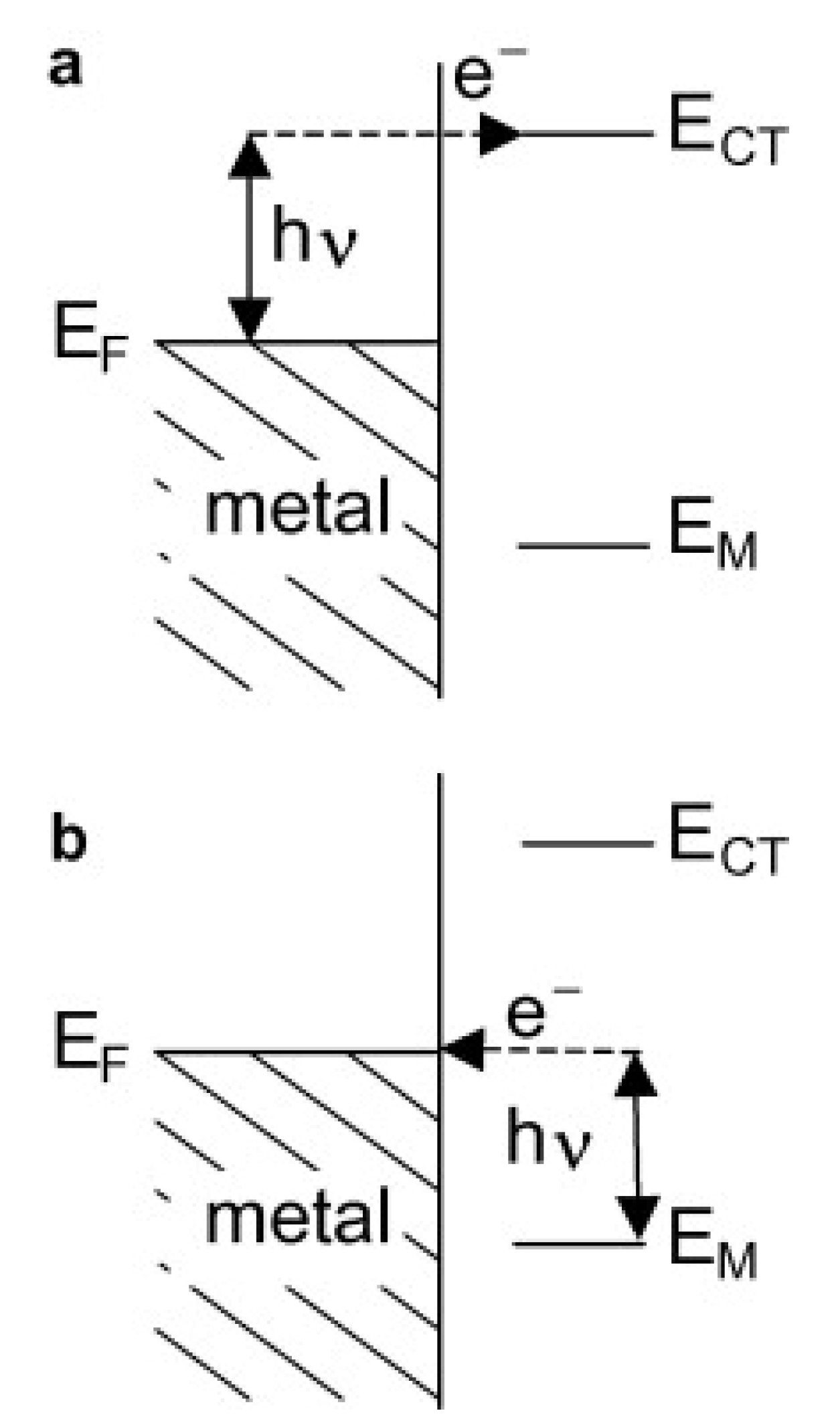
The second enhancement mechanism, which also leads to an increase in the efficiency of the generation of the Raman signal, is called the chemical enhancement. The interaction of adsorbed molecules with the metal substrate provides new electronic transitions for metal (or adsorbed molecule) electrons. The electrons at the Fermi level of the metal can be virtually excited into unoccupied molecular orbitals of the adsorbed molecule and back to the metal (see Figure 2a), or the electrons at the highest occupied molecular orbital can be virtually excited into the Fermi level of the metal and back to the adsorbed molecule (see Figure 2b). This means that a mechanism analogous for the standard resonance Raman process (that can generate a significant increase in the efficiency of the generation of the Raman signal) may be observed for adsorbed molecules[12].
The enhancement of the SERS spectrum in relation to the normal Raman spectrum determines how big enhancement material can provide for the molecule under study. The enhancement factor is given by the formula (Equation 2):

Where: ISERS - intensity of measured SERS spectrum; IRaman - intensity of measured normal Raman spectrum; NRaman - the average number of molecules interacting in normal Raman spectrum; Nsers - the average number of molecules interacting in SERS spectrum
To record the SERS spectrum, Raman scatterers (studied molecules) must be adsorbed at or be placed in a close proximity to the SERS-active material. The first surface-enhanced Raman spectra were published in 1974—in this case, the measurements were carried out on nanostructured silver[5]. During the next three decades, the SERS measurements were also carried out mainly on nanostructured plasmonic metals (Ag, Au and Cu), although other SERS substrates were also developed relatively quickly: in 1982, Loo recorded SERS spectra using as a SERS-active material polycrystalline TiO2[13] and in 1983, Yamada and Yamamoto produced SERS-active materials by the deposition of some metals on the surface of NiO and TiO2[14]. The number of SERS measurements carried out on composite substrates containing non-metallic nanostructured materials are still increasing. This is due to many significant advances of such SERS substrates in some applications of SERS spectroscopy, such composites usually have additional important functionalities that are not possible to obtain in standard SERS substrates produced only from plasmonic metals. In this review article, we present selected SERS substrates that utilize nanostructured non-metallic materials, including non-metallic nanostructured thin films or non-metallic nanoparticles covered by plasmonic metals and SERS-active nanomaterials that do not contain plasmonic metals. Some future perspectives of the application of composite SERS substrates are also discussed.
2. Substrates for Surface-Enhanced Raman Scattering Formed on Nanostructured Non-Metallic Materials
SERS spectroscopy is one of the most sensitive analytical tools. In some cases, the generated SERS signal is so strong that it is possible to record a reliable SERS spectrum even of a single molecule. Therefore, SERS experiments are carried out by a very large number of research groups. To obtain a SERS spectrum, the studied molecules must be adsorbed on a SERS-active substrate (or placed at a very close distance to such a substrate). The quality of measured SERS spectra is closely correlated with the activity of used SERS substrates. In this review article, selected SERS substrates that utilize nanostructured non-metallic materials are described. Recently, one can observe a significant progress in the construction of such a type of nanomaterials. Obtained materials, even those that do not contain plasmonic metals, can generate very large SERS enhancement factors—in some cases similar to those generated on standard SERS substrates produced from pure gold or silver. Moreover, SERS substrates that utilize nanostructured non-metallic materials are often significantly more reproducible than the standard metallic SERS substrates. They can also have some additional functionalities, for example, they can very effectively self-clean when illuminated with UV radiation or can be manipulated by a magnetic field (in the case of magnetic–plasmonic composites), which significantly facilitates their homogenous deposition and removal after the measurement. Therefore, we think that SERS substrates that utilize nanostructured non-metallic materials are a very promising group of nanomaterials and we expect a significant continuous development in this field in the near future—especially in the development of multifunctional SERS substrates, and those designed for specific applications. The strengths and weaknesses of different types of SERS substrates formed from nanostructured non-metallic materials are listed in Table 1.
Table 1. Comparison of different types of SERS substrates formed from nanostructured non-metallic materials.
| Material | Strengths | Weaknesses |
|---|---|---|
| non-metallic nanostructured thin films covered by plasmonic metals | usually high reproducibility, usually high SERS enhancement factors | domination of the measured spectrum by the contribution from molecules interacting directly with the plasmonic metal |
| non-metallic nanoparticles covered by plasmonic metals | usually high SERS enhancement factors, easy possibility to add additional functionalities | domination of the measured spectrum by the contribution from molecules interacting directly with the plasmonic metal |
| SERS substrates that do not contain nanostructured metals | measured SERS spectrum from molecules interacting directly with the analysed material | often low SERS enhancement factors |
References
- Aroca, Ricardo. Surface‐Enhanced Vibrational Spectroscopy; John Wiley & Sons Ltd.: Chichester, 2017; pp. 1.
- M. Fleischmann; P.J. Hendra; A.J. McQuillan; Raman spectra of pyridine adsorbed at a silver electrode. Chemical Physics Letters 1974, 26, 163-166, 10.1016/0009-2614(74)85388-1.
- David L. Jeanmaire; Richard P. Van Duyne; Surface raman spectroelectrochemistry. Journal of Electroanalytical Chemistry and Interfacial Electrochemistry 1977, 84, 1-20, 10.1016/s0022-0728(77)80224-6.
- M. Grant Albrecht; J. Alan Creighton; Anomalously intense Raman spectra of pyridine at a silver electrode. Journal of the American Chemical Society 1977, 99, 5215-5217, 10.1021/ja00457a071.
- Karol Kołątaj; Jan Krajczewski; Andrzej Kudelski; Plasmonic nanoparticles for environmental analysis. Environmental Chemistry Letters 2020, 18, 529-542, 10.1007/s10311-019-00962-1.
- K. Lance Kelly; Eduardo Coronado; Lin Lin Zhao; George C. Schatz; The Optical Properties of Metal Nanoparticles: The Influence of Size, Shape, and Dielectric Environment. The Journal of Physical Chemistry B 2003, 107, 668-677, 10.1021/jp026731y.
- Encai Hao; George C. Schatz; Joseph T. Hupp; Synthesis and Optical Properties of Anisotropic Metal Nanoparticles. Journal of Fluorescence 2004, 14, 331-341, 10.1023/b:jofl.0000031815.71450.74.
- Encai Hao; George C. Schatz; Electromagnetic fields around silver nanoparticles and dimers. The Journal of Chemical Physics 2004, 120, 357-366, 10.1063/1.1629280 10.1063/1.1629280.
- Kelsey A. Stoerzinger; Warefta Hasan; Julia Y. Lin; Alex Robles; Teri W. Odom; Screening Nanopyramid Assemblies to Optimize Surface Enhanced Raman Scattering. The Journal of Physical Chemistry Letters 2010, 1, 1046-1050, 10.1021/jz100095b.
- Jing Yang; Fanghui Ren; Xinyuan Chong; Donglei Fan; Swapnajit Chakravarty; Zheng Wang; Ray T. Chen; Alan X. Wang; Guided-Mode Resonance Grating with Self-Assembled Silver Nanoparticles for Surface-Enhanced Raman Scattering Spectroscopy. Photonics 2014, 1, 380-389, 10.3390/photonics1040380.
- Prathamesh Pavaskar; Jesse Theiss; Stephen B. Cronin; Plasmonic hot spots: nanogap enhancement vs. focusing effects from surrounding nanoparticles.. Optics Express 2012, 20, 14656-14662, 10.1364/oe.20.014656.
- Andrzej Kudelski; Raman spectroscopy of surfaces. Surface Science 2009, 603, 1328-1334, 10.1016/j.susc.2008.11.039.
- B.H. Loo; Observation of the surface enhanced raman scattering effect from the semiconductor—electrolyte interface. Journal of Electroanalytical Chemistry and Interfacial Electrochemistry 1982, 136, 209-213, 10.1016/0022-0728(82)87037-x.
- H. Yamada; Y. Yamamoto; Surface enhanced Raman scattering (SERS) of chemisorbed species on various kinds of metals and semiconductors. Surface Science 1983, 134, 71-90, 10.1016/0039-6028(83)90312-6.

