 +1 credit
| Version | Summary | Created by | Modification | Content Size | Created at | Operation |
|---|---|---|---|---|---|---|
| 1 | Jang-Ung Park | + 3995 word(s) | 3995 | 2021-02-04 07:21:06 | | | |
| 2 | Rita Xu | -631 word(s) | 3364 | 2021-02-09 10:03:30 | | |
Video Upload Options
The development of wearable sensors is aimed at enabling continuous real-time health monitoring, which leads to timely and precise diagnosis anytime and anywhere. Unlike conventional wearable sensors that are somewhat bulky, rigid, and planar, research for next-generation wearable sensors has been focused on establishing fully-wearable systems. To attain such excellent wearability while providing accurate and reliable measurements, fabrication strategies should include (1) proper choices of materials and structural designs, (2) constructing efficient wireless power and data transmission systems, and (3) developing highly-integrated sensing systems.
1. Introduction
Wearable sensors have attracted significant interest due to their potential ability to provide continuous, real-time health monitoring of various physiological parameters [1][2][3][4][5]. Such ability provides real-time feedbacks on daily diets, activities, and physiological conditions, allowing timely and appropriate control and treatments [6][7]. However, current commercial wearable devices such as smartwatches, wristbands or glasses, are usually just miniaturized forms of conventional electronics that consist of rigid, bulky, and planar components. Such rigidity and bulkiness could not only make the devices obtrusive and disturbing but also restrict the conformal contact of the devices to the human body. In particular, this incomplete contact might result in inaccurate measurements and large noises affected by body movements and environmental conditions [2].
Current research has focused on constructing fully-wearable sensing systems, as depicted in Figure 1. To establish such systems, soft materials, wireless technologies, and high integrity are important factors. There has been significant progress in soft, stretchable, and flexible conducting materials, and this has stimulated the development of wearable devices. Soft conducting materials could enhance the compliance of the device to the human body; therefore, they can not only mitigate the disturbance and obtrusiveness on human skin but also enhance the operational reliability [3][6][8][9]. Wireless power supply and data transmission technologies have also been developed significantly and attempt to incorporate those technologies have been made extensively [10]. Wireless power transfer has advantages in that they only require a simple antenna circuit on the power receiving device, which offers a wide selection of materials and structures. Energy harvesters using tribo- and piezoelectric mechanisms enable the charging of electricity through body movement, thus provides an easy way of charging irrespective of the environmental conditions [11][12][13]. Progress in wireless communication technologies and electronic engineering facilitates the data processing-transmission procedure with a miniaturized single electronic chip. Among various wireless communication protocols, near-field communication (NFC) and Bluetooth low energy (BLE) have been used most commonly in wearable devices. Their high compatibility with commercial electronic devices, such as smartphones enables easy and simple data recording without any other display devices attached to the sensor [14][15][16]. Combining all the functional components with varying functions, properties, and shapes into small, compact devices should involve careful and elaborate methodological approaches. The integration should form a configuration suitable for each platform and target function such that they can offer convenient and reliable diagnostics.
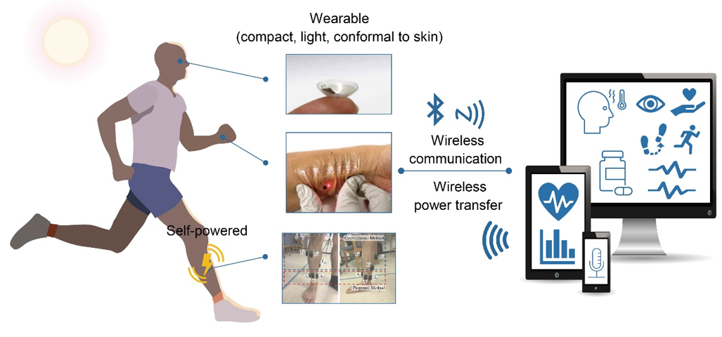
Figure 1. Schematics illustrating the recent progress in wearable devices for non-invasive diagnosis. (top: reprinted with permission from [14]. Copyright 2020 American Association for the Advancement of Science; meddle: reprinted with permission from [17]. Copyright 2019 John Wiley and Sons; bottom: reprinted with permission from [18]. Copyright 2019 MDPI)
2. Nano/Microfabrication Techniques
Various nano/microfabrication techniques including physical vapor deposition (PVD), chemical vapor deposition (CVD), electrodeposition, lithography, and printing have been extensively studied and used for the fabrication of wearable devices. We recommend the readers refer to the following review papers to find more detailed descriptions on the processes and properties of the techniques [19][20][21][22][23].
PVD including thermal evaporation, electron-beam (e-beam) evaporation, and sputtering is widely used for the deposition of metal and metal oxide-based materials into thin films on substrates [24][25][26][27]. Polymer solutions and dispersions of various conducting materials such as metal particles, metal wires, or graphene can be deposited onto diverse matrices and substrates using techniques such as spin-coating, vacuum filtration, and spraying [28][29][30][31]. The adhesion between the deposited materials and the matrices is achieved by chemisorption or physisorption, and to enhance the adhesion and compatibility between them, surface treatments including O2 plasma and silane coupling reaction are widely exploited [32][33]. Electrodeposition is a process of forming thin films of metal-based materials or polymers by applying electric current onto a conductive material that is immersed in a solution containing precursors such as metal salts, monomeric or polymeric materials [34][35][36]. Processing temperatures, chemical resistances of substrates and the deposited materials, the required thickness and the uniformity of the deposition, and the geometrical properties of the substrate matrices are various factors to consider for the selection of deposition techniques. For instance, many flexible or stretchable substrates such as PDMS are susceptible to thermal expansion and contraction under temperature variations, which may cause damages on the deposited metal layers, thus favoring low-temperature processes [37].
For the patterning of deposited layers, photolithography that consists of UV exposure, wet etching or dry etching steps, and e-beam lithography are the most widely used techniques [38][39][40]. These techniques allow high-resolution patterning with nm scale feature sizes for e-beam lithography and tens of nm to µm scale feature sizes for photolithography but have disadvantages of high-cost and small patterning area [90]. E-beam lithography provides low throughput compared with other fabrication techniques. Printing techniques such as screen printing, roll-to-roll printing, and inkjet printing are also extensively used for the nano/microfabrication of flexible and stretchable devices [41][42][43][44]. In screen printing, inks are deposited and spread on to the mask that is placed and aligned onto a substrate, thus resulting in a selective and templated deposition of the ink onto the desired sites of the substrates [45][46]. The screen printing technique is compatible with diverse matrices including textiles, elastomers, and paper, and the minimum feature sizes that can be obtained using the technique are usually tens of µm, but highly dependent upon the composition of ink and particle sizes [47][48][49]. Direct writing and 3D printing enable the patterning of various materials onto substrates of diverse geometries and compositions [50][51][52]. Park et al. demonstrated high-resolution and reconfigurable 3D printing of liquid metal using direct printing as shown in Figure 2i [53]. The resolution of printing was controlled by the diameter of nozzles, and the minimum line width of 1.9 µm was obtained reliably. The printed liquid metal could be lifted-up and relocated by the nozzle tip to form 3D structures. Soft lithography uses elastomeric molds and stamps that are patterned and engraved into desired patterns to produce patterns of various materials as shown in Figure 2h, which allows relatively simple and quick replication, large pattern areas, and low-cost processing [54][55].
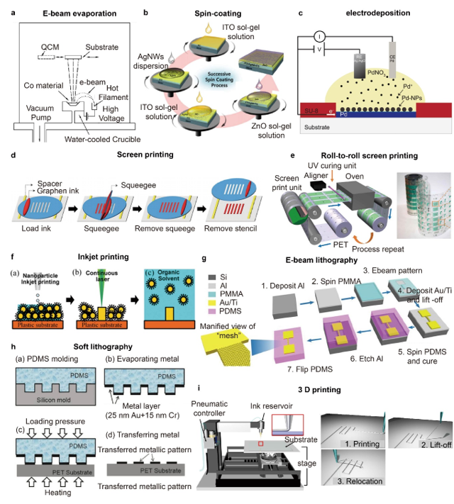
Figure 2. (a) Schematic Illustration of an e-beam evaporation system (reprinted with permission from [27]. Copyright 2004 American Vacuum Society); (b) Schematic illustrations of the successive spin coating ofITO, AgNWs, and ZnO dispersions (reprinted with permission from [31]. Copyright 2015 Royal Society of Chemistry); (c) Schematic illustration showing the electrodeposition of palladium nanoparticles (PdNPs) (reprinted with permission from [34]. Copyright 2019 John Wiley and Sons); (d) Schematic illustrations showing the process of screen printing using a silicon stencil and a pristine graphene ink (reprinted with permission from [46]. Copyright 2015 John Wiley and Sons); (e) (Left) Schematic illustrations of roll-to-roll rotary screen printing of electrodes for sweat sensing patches and (right) an optical image of the as-fabricated sensing electrode patterns (reprinted with permission from [45]. Copyright 2019 The American Association for the Advancement of Science); (f) Schematic illustrations of inkjet printing and patterning of AgNPs using laser sintering (reprinted with permission from [41]. Copyright 2017 John Wiley and Sons); (g) Schematic illustrations demonstrating the fabrication process of high-resolution gold patterns onto elastomer using spin-coating, e-beam lithography and etching (reprinted with permission from [39]. Copyright 2018 Springer Nature); (h) Schematic illustrations of soft lithography involving PMDS molding, metal deposition and metal pattern transfer (reprinted with permission from [55]. Copyright 2017 MDPI); (i) (Left) Schematic illustrations of the 3D direct printing system and (right) printing, lift-up and relocation steps (reprinted with permission from [53]. Copyright 2019 The American Association for the Advancement of Science).
3. Sensors
Various physical properties of the body can be recorded through the different physical variables presented in the external organs of the body. Highly flexible and stretchable bioelectronics that can have conformal contact with the soft, dynamic, and deformable portions of the body are used as wearable sensors for multi-purpose diagnoses of the human body. These sensors have one or more sensing components that can receive various signals of physical, electrophysiological, and biochemical significance for the long-term monitoring of various health conditions. These sensors are devised to be region-specific, and they experience little interference due to the movement of the body.
3.1. Physical Sensors
One of the fundamental conventional parameters of the body that have strong diagnostic significance are physical parameters such as movement-induced strain and temperature. These physical parameters vary temporally and spatially, hence the issues of specificity and accuracy are important when devising such physical sensors. In addition, such parameters are recorded primarily from the skin or they can be incorporated into clothing and artificial epidermal substrate for sensing purposes. Other research has focused on bodily kinetics and muscle activity to study the effect of various diseases that affect the movement of the body, such as cerebral palsy.
The promising aspect of physical sensors is that the devices have stretchable electronics that can detect human motions and perform surface strain calculations. These devices can be incorporated intrinsically into clothing or directly onto the surface of the skin to detect the strain derived from bodily motion. Yamada et al. demonstrated a wearable sensor of single-walled carbon nanotubes that was capable of measuring strains up to 280% [56]. Figure 5a show a photograph of the actual device on synthetic clothes. This sensor can differentiate various aspects of human motion, such as movement, breathing, speech, and typing. This paves the way for an additional wide range of wearable electronics for non-invasive physical sensors. Another work that demonstrates the potential of detecting bodily movement using a wearable sensor was presented by Wang et al. using an ionic liquid microband, as shown in Figure 5b [57]. This intrinsically-stretchable pressure sensor uses nanomaterials and a flexible semiconductor to fabricate a rubber band-like stretchable pressure sensor that is light and thermally sensitive. The use of a non-volatile material also reduces the complexity of the fabrication, and the device showed the detection of strains in the range of 0.1% to 500%, even during multiple repeating cycles. This device can be integrated seamlessly into woven commercial bracelets for the detection of hand gestures, and it even can identify wrist pulses. Work to develop epidermal electronics for a non-invasive physical sensor is a novel component of non-invasive wearable electronics. Tattoo electronics are key devices of such classes due to the seamless infrastructure when they are integrated for application. The work reported by Kim et al. introduced a conformal, contact-based system that shows the great applicability of epidermal tattoo electronics [58]. When incorporated with various sensor systems, the epidermal device can detect various physical variables of the skin, such as temperature and strain.

Figure 5. (a) A photograph of stretchable carbon nanotube strain sensor attached to clothing to detect physical motion (reprinted with permission from [56]. Copyright 2011 Springer Nature); (b) Ionic liquid-based sensor patch of cervical movement detection for directional strain calculation of skin during neck movement (reprinted with permission from [57]. Copyright 2014 Royal Society of Chemistry); (c) Commercial epidermal tattoo with the integrated circuit at its backside for multifunctional application (reprinted with permission from [58]. Copyright 2011 American Association for the Advancement of Science); (d) Photo of the patient using exoskeleton assisted knee extension on an instrumented treadmill (reprinted with permission from [59]. Copyright 2017 Spring Nature); (e) (Top) EEG electrode with a tripolar concentric ring with an integrated capacitive design. (Bottom) Images of ring electrodes on the skin for EEG measurement (reprinted with permission from [60]. Copyright 2015 National Academy of Sciences); (f) (Left) A photograph of plasticized silk electrode on human forearm for EMG measurement. (Right) EMG signals obtained by silk electrode during muscle movement with comparison to commercial gem electrodes (reprinted with permission from [61]. Copyright 2018 John Wiley and Sons); (g) (Left) Colorimetric detection reservoirs for water lactate, glucose, creatinine, pH, and chloride ions in a wearable microfluidic device. (Right) Images of epidermal microfluidic electrochemical sensor after injection of artificial sweat (reprinted with permission from [62]. Copyright 2016 The American Association for the Advancement of Science); (h) Glucose detecting mechanism schematics of a skin-like sensor using an electrochemical twin channel (reprinted with permission from [63]. Copyright 2017 The American Association for the Advancement of Science).
To reinforce the concept of the physical sensor, work to integrate physical sensors for the training and rehabilitation of muscles also shows signs of increasing importance. Fiber-shaped strain sensors can be integrated into woven textile materials for real-time mechanical feedback of surface strain detection. These stretchable sensors can be used to monitor sports activity when attached to an athlete’s body [64]. Work to improve the usability of these surface strain sensors was developed further by integrating them into the exoskeleton. The knee extension-assisted exoskeleton developed by Lerner et al. shows that the device can help rehabilitate patients with cerebral palsy and weakened muscle activity [59]. With the onset of cerebral palsy commonly occurring during childhood, the importance of addressing the implication of such disease comes early. The work that has been presented shows evidence of improvement in the dynamic gait posture and the rehabilitative impact of limb joint mechanics in patients using the robotic exoskeleton. The demonstration of the actual rehabilitation process using this device is shown in Figure 5d. The deep mechanical analysis of patient movement during the rehabilitation process also shows promising insight into the study and clinical modeling of cerebral palsy. With these mechanical physical sensors, the long-term investigation of disease and mechanical rehabilitation can be conducted non-invasively.
3.2. Electrophysiological Sensors
Another variety of non-invasive sensors are the electrophysiological sensors that collect bodily electrical signals, such as the ECG [65][66], electroencephalogram (EEG) [67][68], and electromyography (EMG) [69][70]. The capability of continuous physiological monitoring is needed for the treatment and diagnosis of medical conditions. The issue related to the acquisition, filtering, amplification, and radio frequency (RF) transmission of data must be optimized for precise electrophysiological characterization. Hence, epidermal sensors have been developed that can seamlessly access the physiological data of the body. These sensors usually are composed of a soft, stretchable substrate with a biocompatible electrode that has a curvilinear structure.
The study of the bioelectrical signals of the body has been extremely important in the early diagnosis of disease and its symptoms. In the case of cardiovascular diseases, the abrupt and random occurrences of heart attacks may require constant recording and monitoring of electrophysiological signals. Most commercial devices require hospitalization and the use of an invasive diagnostics device that can cause secondary complications. Lee et al. developed a thin electronic device that, when placed on the epidermis, is capable of self-adhesion [71]. This device is integrated with commercial electronic components and uses carbon nanotubes to retain conformal contact with the wrinkles of the skin without any motion artifacts. The use of carbon nanotubes has resulted in a drastic lowering of the overall modulus of the device. This enhanced flexibility of the device enables the collection of reliable ECG data, and it has an overall performance that is superior to that of the rigid, capacitive-type electrode. Xu et al. also demonstrated the use of a low-modulus, elastic, epidermal sensor for recording ECGs [72]. They used controlled mechanical buckling and soft microfluidics to fabricate ultra-low modulus devices that are intrinsically stretchable. They also demonstrated the concept of collecting data wirelessly, which is very important for the inconspicuous operation of epidermal electrophysiological sensors.
Recent advances in non-invasive EEG devices have shown long-term operation and minimal loading contact. EEG devices, in particular, are mounted onto the auricle and mastoid surface, which requires minimal thermal, mechanical, and electrical damage to the skin. In addition, the high irregularity of the surface of the auricle requires detailed structural planning for the bending and stretching of these EEG devices. The non-invasive epidermal EEG developed by Norton et al. has a wearable EEG sensor that remains mounted conformally during vigorous exercise [60]. Figure 5e shows the conformal attachment of the device to the skin when the device is mounted. The device has shown the features of non-invasive interfaces to the skin that show reliable EEG recording and the possibility of wireless integration. Admittedly, there is room for the amplification of the signal and improved accuracy since EEG signals usually are small and difficult to trace. To detect detection the electrical activity produced by a skeletal muscle, EMG signals usually are recorded on the surface of the skin directly above the targeted muscle. Chen et al. showed an example of an EMG skin device that used silk protein substrate for a soft and stretchable sensor device that could be integrated seamlessly, as shown in Figure 5f [61]. The device had high electrical performance and conformality when it was used as an epidermal electronic sensor.
3.3. Biochemical Sensors
Another category of the non-invasive sensor is the chemical analysis of ions, biomolecules, electrolytes, and proteins present in bodily fluids. The modern clinical examination uses blood samples for biochemical assessment for various diseases and conditions. But for non-invasive sensors, sweat and its ionic composition are the main targets for quantitative biochemical analysis. This almost completely removes the need for the invasive collection of samples that can cause psychological trauma or problematic infections. Such electrochemical sensors usually are composed of soft, stretchable, microfluidic systems with specialized receptors that interact with the target ions. These receptors are usually enzymes or antibodies that have a specific color or a change in pH when they react with the target ions.
The characterization and biochemical analysis of biofluids, such as sweat, can be deemed to have high clinical value when complemented with other physical characteristics. Due to the relative ease of non-invasive sample collection, sweat is a representative biofluid that is full of intricate biomarkers. Koh et al. demonstrated a soft, wearable microfluidic device that was capable of capturing and storing sweat for electrochemical analysis [62]. The device, which is shown in Figure 5g, allows the quantitative collection of sweat rates, pH variations, and changes in the concentrations of biomarkers. The changes in the biomarkers are analyzed by colorimetry, and the test is conducted during a controlled fitness cycle. The epidermal microfluidic device can evaluate the performances of athletes while monitoring various other markers of health status. Key markers, such as creatinine, lactate, chloride, glucose, and pH, are evaluated without the device losing its adhesion to failing to operate correctly. Another perspiration-based biochemical sensor was developed by Emaminehad et al., and it evaluates the variables related to cystic fibrosis for diagnostic purposes [73]. The electrolyte contents of the sweat of cystic fibrosis patients were obtained through non-invasive methods using sweat collected by the sensor. The device is composed of a miniaturized iontophoresis interface that delivers stimulating agonist to sweat glands via an electrical current. The correlation between the concentration of the drug and the rate of sweating has been demonstrated for clinical modeling with reliable stability of the device and user conformality. It also introduced a preliminary study of metabolic glucose content between sweat and blood. The culmination of the sweat profiles of individuals can enable future integration into large-scale clinical investigations for more extensive biomedical modeling. Another notable work that utilizes sweat for non-invasive recording is the textile-based potentiometric sensor developed by Parrilla et al. for the analysis of multiple ions in sweat [74]. The incorporation of a polyurethane-based, ion-selective membrane with a stretchable ink electrode strengthens the conductivity and biocompatibility of the textile-based sensors. The integration of stretchable ink and components with serpentine design has greatly enhanced the durability of tensile stress. Despite the practicality of sweat-based sensors, there are issues related to the uncertainties associated with the device due to the presence of other biofluids and markers because they limit the impact of the biomedical applications for non-invasive sampling.
To supplement the mentioned uncertainty associated with monitoring sweat, Chen et al. developed a skin-like, non-invasive sensor for the highly-accurate monitoring of glucose in blood [63]. The device has integrated subcutaneous channels that drive intravascular blood glucose to the surface of the skin. The epidermal glucose detecting mechanism is shown in Figure 5h. This additional augmentation does not comprise the conformality of the device, and it provides prospects for high standard clinical application. When the reliability of the device is optimized to the medical-grade standard, the potential possibility of insulin therapy will be opened with further expansion of the application prospective of non-invasive electrochemical sensors.
References
- Kim, J.; Campbell, A.S.; de Ávila, B.E.-F.; Wang, J. Wearable Biosensors for Healthcare Monitoring. Biotechnol. 2019, 37, 389–406, doi:10.1038/s41587-019-0045-y.
- Gao, Y.; Yu, L.; Yeo, J.C.; Lim, C.T. Flexible Hybrid Sensors for Health Monitoring: Materials and Mechanisms to Render Wearability. Mater. 2020, 32, 1902133, doi:10.1002/adma.201902133.
- Lim, H.-R.; Kim, H.S.; Qazi, R.; Kwon, Y.-T.; Jeong, J.-W.; Yeo, W.-H. Advanced Soft Materials, Sensor Integrations, and Applications of Wearable Flexible Hybrid Electronics in Healthcare, Energy, and Environment. Mater. 2020, 32, 1901924, doi:10.1002/adma.201901924.
- Wen, F.; He, T.; Liu, H.; Chen, H.-Y.; Zhang, T.; Lee, C. Advances in Chemical Sensing Technology for Enabling the Next-Generation Self-Sustainable Integrated Wearable System in the IoT Era. Nano Energy 2020, 78, 105155, doi:10.1016/j.nanoen.2020.105155.
- Gao, W.; Ota, H.; Kiriya, D.; Takei, K.; Javey, A. Flexible Electronics toward Wearable Sensing. Accounts Chem. Res. 2019, 52, 523–533, doi:10.1021/acs.accounts.8b00500.
- Ling, Y.; An, T.; Yap, L.W.; Zhu, B.; Gong, S.; Cheng, W. Disruptive, Soft, Wearable Sensors. Mater. 2020, 32, 1904664, doi:10.1002/adma.201904664.
- Ray, T.R.; Choi, J.; Bandodkar, A.J.; Krishnan, S.; Gutruf, P.; Tian, L.; Ghaffari, R.; Rogers, J.A. Bio-Integrated Wearable Systems: A Comprehensive Review. Rev. 2019, 119, 5461–5533, doi:10.1021/acs.chemrev.8b00573.
- Liu, Y.; Pharr, M.; Salvatore, G.A. Lab-on-Skin: A Review of Flexible and Stretchable Electronics for Wearable Health Monitoring. ACS Nano 2017, 11, 9614–9635, doi:10.1021/acsnano.7b04898.
- Kim, K.; Park, Y.-G.; Hyun, B.G.; Choi, M.; Park, J.-U. Recent Advances in Transparent Electronics with Stretchable Forms. Mater. 2019, 31, 1804690, doi:10.1002/adma.201804690.
- Kassal, P.; Zubak, M.; Scheipl, G.; Mohr, G.J.; Steinberg, M.D.; Murković Steinberg, I. Smart Bandage with Wireless Connectivity for Optical Monitoring of PH. Actuators B Chem. 2017, 246, 455–460, doi:10.1016/j.snb.2017.02.095.
- Hu, L.; Wu, H.; La Mantia, F.; Yang, Y.; Cui, Y. Thin, Flexible Secondary Li-Ion Paper Batteries. ACS Nano 2010, 4, 5843–5848, doi:10.1021/nn1018158.
- Sun, L.; Chen, S.; Guo, Y.; Song, J.; Zhang, L.; Xiao, L.; Guan, Q.; You, Z. Ionogel-Based, Highly Stretchable, Transparent, Durable Triboelectric Nanogenerators for Energy Harvesting and Motion Sensing over a Wide Temperature Range. Nano Energy 2019, 63, 103847, doi:10.1016/j.nanoen.2019.06.043.
- Chen, X.; Song, Y.; Su, Z.; Chen, H.; Cheng, X.; Zhang, J.; Han, M.; Zhang, H. Flexible Fiber-Based Hybrid Nanogenerator for Biomechanical Energy Harvesting and Physiological Monitoring. Nano Energy 2017, 38, 43–50, doi:10.1016/j.nanoen.2017.05.047.
- Ku, M.; Kim, J.; Won, J.-E.; Kang, W.; Park, Y.-G.; Park, J.; Lee, J.-H.; Cheon, J.; Lee, H.H.; Park, J.-U. Smart, Soft Contact Lens for Wireless Immunosensing of Cortisol. Adv. 2020, 6, eabb2891, doi:10.1126/sciadv.abb2891.
- Park, J.; Kim, J.; Kim, S.-Y.; Cheong, W.H.; Jang, J.; Park, Y.-G.; Na, K.; Kim, Y.-T.; Heo, J.H.; Lee, C.Y.; et al. Soft, Smart Contact Lenses with Integrations of Wireless Circuits, Glucose Sensors, and Displays. Adv. 2018, 4, eaap9841, doi:10.1126/sciadv.aap9841.
- Bandodkar, A.J.; Gutruf, P.; Choi, J.; Lee, K.; Sekine, Y.; Reeder, J.T.; Jeang, W.J.; Aranyosi, A.J.; Lee, S.P.; Model, J.B.; et al. Battery-Free, Skin-Interfaced Microfluidic/Electronic Systems for Simultaneous Electrochemical, Colorimetric, and Volumetric Analysis of Sweat. Adv. 2019, 5, eaav3294, doi:10.1126/sciadv.aav3294.
- Jeong, H.; Wang, L.; Ha, T.; Mitbander, R.; Yang, X.; Dai, Z.; Qiao, S.; Shen, L.; Sun, N.; Lu, N. Modular and Reconfigurable Wireless E-Tattoos for Personalized Sensing. Mater. Technol. 2019, 4, 1900117, doi:10.1002/admt.201900117.
- Isezaki, T.; Kadone, H.; Niijima, A.; Aoki, R.; Watanabe, T.; Kimura, T.; Suzuki, K. Sock-Type Wearable Sensor for Estimating Lower Leg Muscle Activity Using Distal EMG Signals. Sensors 2019, 19, 1954, doi:10.3390/s19081954.
- Li, Q.; Zhang, J.; Li, Q.; Li, G.; Tian, X.; Luo, Z.; Qiao, F.; Wu, X.; Zhang, J. Review of Printed Electrodes for Flexible Devices. Front. Mater. 2019, 5.
- Herrer, L.; Martín, S.; Cea, P. Nanofabrication Techniques in Large-Area Molecular Electronic Devices. Appl. Sci. 2020, 10, 6064.
- Kang, K.; Cho, Y.; Yu, K.J. Novel Nano-Materials and Nano-Fabrication Techniques for Flexible Electronic Systems. Micromachines 2018, 9, 263.
- Pimpin, A.; Srituravanich, W. Review on Micro- and Nanolithography Techniques and Their Applications. Eng. J. 2012, 16, 37–56.
- Du, K.; Ding, J.; Liu, Y.; Wathuthanthri, I.; Choi, C.-H. Stencil Lithography for Scalable Micro- and Nanomanufacturing. Micromachines 2017, 8, 131.
- Fu, R.; Yang, Y.; Lu, C.; Ming, Y.; Zhao, X.; Hu, Y.; Zhao, L.; Hao, J.; Chen, W. Large-Scale Fabrication of High-Performance Ionic Polymer–Metal Composite Flexible Sensors by in Situ Plasma Etching and Magnetron Sputtering. ACS Omega 2018, 3, 9146–9154.
- Gao, W.; Nyein, H.Y.Y.; Shahpar, Z.; Fahad, H.M.; Chen, K.; Emaminejad, S.; Gao, Y.; Tai, L.-C.; Ota, H.; Wu, E.; et al. Wearable Microsensor Array for Multiplexed Heavy Metal Monitoring of Body Fluids. ACS Sens. 2016, 1, 866–874.
- Son, D.; Lee, J.; Qiao, S.; Ghaffari, R.; Kim, J.; Lee, J.E.; Song, C.; Kim, S.J.; Lee, D.J.; Jun, S.W.; et al. Multifunctional Wearable Devices for Diagnosis and Therapy of Movement Disorders. Nat. Nanotechnol. 2014, 9, 397–404.
- Ding, Z.; Thibado, P.M.; Awo-Affouda, C.; LaBella, V.P. Electron-Beam Evaporated Cobalt Films on Molecular Beam Epitaxy Prepared GaAs(001). J. Vac. Sci. Technol. B Microelectron. Nanometer Struct. 2004, 22, 2068.
- Zhang, S.; Li, Y.; Pan, N. Graphene Based Supercapacitor Fabricated by Vacuum Filtration Deposition. J. Power Sources 2012, 206, 476–482.
- Ly, T.N.; Park, S. Wearable Strain Sensor for Human Motion Detection Based on Ligand-Exchanged Gold Nanoparticles. J. Ind. Eng. Chem. 2020, 82, 122–129.
- Pu, N.-W.; Wang, C.-A.; Liu, Y.-M.; Sung, Y.; Wang, D.-S.; Ger, M.-D. Dispersion of Graphene in Aqueous Solutions with Different Types of Surfactants and the Production of Graphene Films by Spray or Drop Coating. J. Taiwan Inst. Chem. Eng. 2012, 43, 140–146.
- Kim, A.; Lee, H.; Kwon, H.-C.; Jung, H.S.; Park, N.-G.; Jeong, S.; Moon, J. Fully Solution-Processed Transparent Electrodes Based on Silver Nanowire Composites for Perovskite Solar Cells. Nanoscale 2016, 8, 6308–6316.
- Ahmed, S.R.; Kim, J.; Tran, V.T.; Suzuki, T.; Neethirajan, S.; Lee, J.; Park, E.Y. In Situ Self-Assembly of Gold Nanoparticles on Hydrophilic and Hydrophobic Substrates for Influenza Virus-Sensing Platform. Sci. Rep. 2017, 7, 44495.
- Zhou, X.; Zhu, L.; Fan, L.; Deng, H.; Fu, Q. Fabrication of Highly Stretchable, Washable, Wearable, Water-Repellent Strain Sensors with Multi-Stimuli Sensing Ability. ACS Appl. Mater. Interfaces 2018, 10, 31655–31663.
- Strakosas, X.; Selberg, J.; Zhang, X.; Christie, N.; Hsu, P.-H.; Almutairi, A.; Rolandi, M. A Bioelectronic Platform Modulates PH in Biologically Relevant Conditions. Adv. Sci. 2019, 6, 1800935.
- Han, F.; Li, J.; Zhao, S.; Zhang, Y.; Huang, W.; Zhang, G.; Sun, R.; Wong, C.-P. A Crack-Based Nickel@graphene-Wrapped Polyurethane Sponge Ternary Hybrid Obtained by Electrodeposition for Highly Sensitive Wearable Strain Sensors. J. Mater. Chem. C 2017, 5, 10167–10175.
- Lete, C.; Marin, M.; Anghel, E.M.; Preda, L.; Matei, C.; Lupu, S. Sinusoidal Voltage Electrodeposition of PEDOT-Prussian Blue Nanoparticles Composite and Its Application to Amperometric Sensing of H2O2 in Human Blood. Mater. Sci. Eng. C 2019, 102, 661–669.
- Müller, A.; Wapler, M.C.; Wallrabe, U. A Quick and Accurate Method to Determine the Poisson’s Ratio and the Coefficient of Thermal Expansion of PDMS. Soft Matter 2019, 15, 779–784.
- Kim, M.; Park, J.; Ji, S.; Shin, S.-H.; Kim, S.-Y.; Kim, Y.-C.; Kim, J.-Y.; Park, J.-U. Fully-Integrated, Bezel-Less Transistor Arrays Using Reversibly Foldable Interconnects and Stretchable Origami Substrates. Nanoscale 2016, 8, 9504–9510.
- Tan, E.K.W.; Rughoobur, G.; Rubio-Lara, J.; Tiwale, N.; Xiao, Z.; Davidson, C.A.B.; Lowe, C.R.; Occhipinti, L.G. Nanofabrication of Conductive Metallic Structures on Elastomeric Materials. Sci. Rep. 2018, 8, 6607.
- Fabrizio, E.D.; Grella, L.; Baciocchi, M.; Gentili, M.; Ascoli, C.; Cappella, B.; Frediani, C.; Morales, P. Nanometer Biodevice Fabrication by Electron Beam Lithography. J. Vac. Sci. Technol. B Microelectron. Nanometer Struct. 1998, 15, 2892.
- Mattana, G.; Loi, A.; Woytasik, M.; Barbaro, M.; Noël, V.; Piro, B. Inkjet-Printing: A New Fabrication Technology for Organic Transistors. Adv. Mater. Technol. 2017, 2, 1700063.
- Al-Halhouli, A.; Al-Ghussain, L.; El Bouri, S.; Liu, H.; Zheng, D. Fabrication and Evaluation of a Novel Non-Invasive Stretchable and Wearable Respiratory Rate Sensor Based on Silver Nanoparticles Using Inkjet Printing Technology. Polymers 2019, 11, 1518.
- Kooy, N.; Mohamed, K.; Pin, L.T.; Guan, O.S. A Review of Roll-to-Roll Nanoimprint Lithography. Nanoscale Res. Lett. 2014, 9, 320.
- Lübkemann, F.; Miethe, J.F.; Steinbach, F.; Rusch, P.; Schlosser, A.; Zámbó, D.; Heinemeyer, T.; Natke, D.; Zok, D.; Dorfs, D.; et al. Patterning of Nanoparticle-Based Aerogels and Xerogels by Inkjet Printing. Small 2019, 15, 1902186.
- Nyein, H.Y.Y.; Bariya, M.; Kivimäki, L.; Uusitalo, S.; Liaw, T.S.; Jansson, E.; Ahn, C.H.; Hangasky, J.A.; Zhao, J.; Lin, Y.; et al. Regional and Correlative Sweat Analysis Using High-Throughput Microfluidic Sensing Patches Toward Decoding Sweat. Sci. Adv. 2019, 5, eaaw9906.
- Hyun, W.J.; Secor, E.B.; Hersam, M.C.; Frisbie, C.D.; Francis, L.F. High-Resolution Patterning of Graphene by Screen Printing with a Silicon Stencil for Highly Flexible Printed Electronics. Adv. Mater. 2015, 27, 109–115.
- Luo, C.; Tian, B.; Liu, Q.; Feng, Y.; Wu, W. One-Step-Printed, Highly Sensitive, Textile-Based, Tunable Performance Strain Sensors for Human Motion Detection. Adv. Mater. Technol. 2020, 5, 1900925.
- Yáñez-Sedeño, P.; Campuzano, S.; Pingarrón, J.M. Screen-Printed Electrodes: Promising Paper and Wearable Transducers for (Bio)Sensing. Biosensors 2020, 10, 76.
- Sekertekin, Y.; Bozyel, I.; Gokcen, D. A Flexible and Low-Cost Tactile Sensor Produced by Screen Printing of Carbon Black/PVA Composite on Cellulose Paper. Sensors 2020, 20, 2908.
- Galliker, P.; Schneider, J.; Eghlidi, H.; Kress, S.; Sandoghdar, V.; Poulikakos, D. Direct Printing of Nanostructures by Electrostatic Autofocussing of Ink Nanodroplets. Nat. Commun. 2012, 3, 890.
- Yuk, H.; Zhao, X. A New 3D Printing Strategy by Harnessing Deformation, Instability, and Fracture of Viscoelastic Inks. Adv. Mater. 2018, 30, 1704028.
- Seol, S.K.; Kim, D.; Lee, S.; Kim, J.H.; Chang, W.S.; Kim, J.T. Electrodeposition-Based 3D Printing of Metallic Microarchitectures with Controlled Internal Structures. Small 2015, 11, 3896–3902.
- Park, Y.-G.; An, H.S.; Kim, J.-Y.; Park, J.-U. High-Resolution, Reconfigurable Printing of Liquid Metals with Three-Dimensional Structures. Sci. Adv. 2019, 5, eaaw2844.
- Hsu, J.W.P. Soft Lithography Contacts to Organics. Mater. Today 2005, 8, 42–54.
- Su, W.-X.; Wu, C.-Y.; Lee, Y.-C. Waveguide Plasmon Resonance of Arrayed Metallic Nanostructures Patterned on a Soft Substrate by Direct Contact Printing Lithography. Sensors 2017, 17, 1867.
- Yamada, T.; Hayamizu, Y.; Yamamoto, Y.; Yomogida, Y.; Izadi-Najafabadi, A.; Futaba, D.N.; Hata, K. A Stretchable Carbon Nanotube Strain Sensor for Human-Motion Detection. Nat. Nanotechnol. 2011, 6, 296–301.
- Wang, Y.; Gong, S.; Wang, S.J.; Simon, G.P.; Cheng, W. Volume-Invariant Ionic Liquid Microbands as Highly Durable Wearable Biomedical Sensors. Mater. Horiz. 2016, 3, 208–213.
- Kim, D.-H.; Lu, N.; Ma, R.; Kim, Y.-S.; Kim, R.-H.; Wang, S.; Wu, J.; Won, S.M.; Tao, H.; Islam, A.; et al. Epidermal Electronics. Science 2011, 333, 838–843.
- Lerner, Z.F.; Damiano, D.L.; Bulea, T.C. The Effects of Exoskeleton Assisted Knee Extension on Lower-Extremity Gait Kinematics, Kinetics, and Muscle Activity in Children with Cerebral Palsy. Sci. Rep. 2017, 7, 13512.
- Norton, J.J.S.; Lee, D.S.; Lee, J.W.; Lee, W.; Kwon, O.; Won, P.; Jung, S.-Y.; Cheng, H.; Jeong, J.-W.; Akce, A.; et al. Soft, Curved Electrode Systems Capable of Integration on the Auricle as a Persistent Brain–Computer Interface. Proc. Natl. Acad. Sci. USA 2015, 112, 3920–3925.
- Chen, G.; Matsuhisa, N.; Liu, Z.; Qi, D.; Cai, P.; Jiang, Y.; Wan, C.; Cui, Y.; Leow, W.R.; Liu, Z.; et al. Plasticizing Silk Protein for On-Skin Stretchable Electrodes. Adv. Mater. 2018, 30, 1800129.
- Koh, A.; Kang, D.; Xue, Y.; Lee, S.; Pielak, R.M.; Kim, J.; Hwang, T.; Min, S.; Banks, A.; Bastien, P.; et al. A Soft, Wearable Microfluidic Device for the Capture, Storage, and Colorimetric Sensing of Sweat. Sci. Transl. Med. 2016, 8, 366ra165.
- Chen, Y.; Lu, S.; Zhang, S.; Li, Y.; Qu, Z.; Chen, Y.; Lu, B.; Wang, X.; Feng, X. Skin-Like Biosensor System via Electrochemical Channels for Noninvasive Blood Glucose Monitoring. Sci. Adv. 2017, 3, e1701629.
- Liu, Z.; Qi, D.; Hu, G.; Wang, H.; Jiang, Y.; Chen, G.; Luo, Y.; Loh, X.J.; Liedberg, B.; Chen, X. Surface Strain Redistribution on Structured Microfibers to Enhance Sensitivity of Fiber-Shaped Stretchable Strain Sensors. Adv. Mater. 2018, 30, 1704229.
- Nemati, E.; Deen, M.J.; Mondal, T. A Wireless Wearable ECG Sensor for Long-Term Applications. IEEE Commun. Mag. 2012, 50, 36–43.
- Lee, S.M.; Sim, K.S.; Kim, K.K.; Lim, Y.G.; Park, K.S. Thin and Flexible Active Electrodes with Shield for Capacitive Electrocardiogram Measurement. Med. Biol. Eng. Comput. 2010, 48, 447–457.
- Smith, S. EEG in the Diagnosis, Classification, and Management of Patients with Epilepsy. J. Neurol. Neurosurg. Psychiatry 2005, 76, ii2–ii7.
- Babiloni, C.; Del Percio, C.; Arendt-Nielsen, L.; Soricelli, A.; Romani, G.L.; Rossini, P.M.; Capotosto, P. Cortical EEG Alpha Rhythms Reflect Task-Specific Somatosensory and Motor Interactions in Humans. Clin. Neurophysiol. 2014, 125, 1936–1945.
- Shin, S.; Lee, J.; Son, S.H. A Survey of Approaches for Recognizing Hand Gestures Using EMG Signal. In Proceedings of the 2016 IEEE 22nd International Conference on Embedded and Real-Time Computing Systems and Applications (RTCSA), Daegu, Korea, 17–19 August 2016; p. 263.
- Roland, T.; Mairhofer, S.; Roland, W.; Diskus, C.; Amsuess, S.; Russold, M.F.; Wolf, C.; Baumgartner, W. Evaluation of Capacitive EMG Sensor Geometries by Simulation and Measurement. In Scientific Computing in Electrical Engineering; Langer, U., Amrhein, W., Zulehner, W., Eds.; Springer International Publishing: Cham, Switzerland, 2018; pp. 13–23.
- Lee, S.M.; Byeon, H.J.; Lee, J.H.; Baek, D.H.; Lee, K.H.; Hong, J.S.; Lee, S.-H. Self-Adhesive Epidermal Carbon Nanotube Electronics for Tether-Free Long-Term Continuous Recording of Biosignals. Sci. Rep. 2014, 4, 6074.
- Xu, S.; Zhang, Y.; Jia, L.; Mathewson, K.E.; Jang, K.-I.; Kim, J.; Fu, H.; Huang, X.; Chava, P.; Wang, R.; et al. Soft Microfluidic Assemblies of Sensors, Circuits, and Radios for the Skin. Science 2014, 344, 70–74.
- Emaminejad, S.; Gao, W.; Wu, E.; Davies, Z.A.; Nyein, H.Y.Y.; Challa, S.; Ryan, S.P.; Fahad, H.M.; Chen, K.; Shahpar, Z.; et al. Autonomous Sweat Extraction and Analysis Applied to Cystic Fibrosis and Glucose Monitoring Using a Fully Integrated Wearable Platform. Proc. Natl. Acad. Sci. USA 2017, 114, 4625–4630.
- Parrilla, M.; Cánovas, R.; Jeerapan, I.; Andrade, F.J.; Wang, J. A Textile-Based Stretchable Multi-Ion Potentiometric Sensor. Adv. Healthc. Mater. 2016, 5, 996–1001.

