

 +1 credit
| Version | Summary | Created by | Modification | Content Size | Created at | Operation |
|---|---|---|---|---|---|---|
| 1 | Akeem Adeyemi Oladipo | -- | 2043 | 2026-08-06 21:34:13 | | | |
| 2 | Catherine Yang | Meta information modification | 2043 | 2026-08-07 04:43:17 | | |
Video Upload Options
Transduction mechanisms in nanostructured electrochemical sensors dictate how molecular recognition events and physical interactions at an electrode interface are converted into measurable electrical, optical, or photo-driven signals. By engineering sensor architectures across structural scales—from sub-nanometer single-atom catalysts (SACs) and quantum-confined nanoclusters to two-dimensional (2D) materials (MXenes, MOFs, COFs) and three-dimensional (3D) hierarchical porous networks—the governing signal conversion pathways shift fundamentally. These modes encompass direct inner-sphere faradaic charge transfer, electrochemiluminescence (ECL) coreactant pathways, photoelectrochemical (PEC) exciton separation, and field-effect interfacial gating. Understanding and tailoring these cross-scale transduction principles is essential for designing high-sensitivity, selective, and robust bio- and chemical sensors. The key focus herein is the physical chemistry, transport physics, and quantum mechanics underlying these distinct transduction modalities.
1. Introduction
Electrochemical sensors fundamentally rely on the efficient translation of interfacial chemical interactions into quantifiable macroscale electrical signals. Historically, macro-scale or bulk electrodes relied on surface-mediated electron transfer governed by standard continuous-band metallic properties and semi-infinite linear diffusion. However, the integration of nanostructured materials into electroanalytical platforms has fundamentally altered these signal transduction pathways.[1]
By operating across distinct physical regimes—sub-nanometer quantum confinement (0D), two-dimensional atomic layering (2D), and three-dimensional continuous mass-transport channels (3D)—nanomaterials dictate the exact physics of signal conversion.[1] The architectural scale of the active material strictly governs whether charge transfer proceeds via discrete inner-sphere faradaic processes, highly energetic electrochemiluminescence (ECL), photoelectrochemical (PEC) exciton separation, or field-effect charge gating. Developing next-generation, ultra-sensitive analytical devices requires a rigorous mechanistic understanding of how target analytes perturb the local electronic, optical, or ionic environment of these advanced nano-scaffolds.
2. Sub-Nanometer Transduction: Single-Atom & Quantum-Confined Regimes
At the sub-nanometer scale (0D), the classical physics of bulk metals collapse. Materials exhibit quantized electronic energy levels, maximum atomic utilization, and highly localized coordination environments, fundamentally altering traditional electrocatalytic scaling relationships.[1][2]
2.1. Single-Atom Catalysts (SACs) and Inner-Sphere Catalysis
Single-Atom Catalysts (SACs) feature atomically dispersed metal sites (e.g., Fe, Co, Pt) covalently coordinated to a non-metal support matrix, frequently via M-Nx-C configurations. Transduction at SACs proceeds exclusively via inner-sphere faradaic mechanisms, requiring the target analyte to physically adsorb and hybridize with the isolated metal center.[2]
The extreme sensitivity of SACs arises from the narrowing and shifting of the d-band center (εd) relative to the Fermi level (EF). According to d-band theory, the adsorption free energy (ΔGads) of a target analyte dictates the kinetic overpotential (η) of the electrochemical reaction. Unlike bulk nanoparticles, where the continuous d-band dictates rigid scaling relations between intermediates (e.g., locking the energy difference between O* and OH* at a constant ≈3.2 eV), the isolated d-orbitals of SACs break these localized symmetry constraints. This allows for optimal, intermediate-specific binding that minimizes the activation energy barrier (Ea), yielding massive faradaic signal amplification.[2]
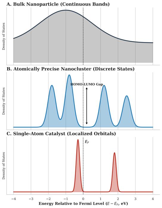
Figure 1. Electronic State Transitions from Bulk to Quantum-Confined Regimes. The Density of States (DOS) simulation demonstrates the transition from continuous metallic bands overlapping the Fermi level in bulk materials, to the opening of a discrete HOMO-LUMO gap in atomically precise nanoclusters, to the sharp, highly localized atomic orbitals characteristic of Single-Atom Catalysts (SACs).
2.2. Dual-Atom Catalysts (D-SACs) and Synergistic Pathways
While SACs provide unparalleled atomic efficiency, they are structurally limited to single-site intermediate adsorption, which restricts complex, multi-electron transfer steps. Dual-Atom Catalysts (D-SACs), featuring adjacent, heteronuclear metal centers (e.g., Fe-Co-N6), resolve this by offering bidentate synergistic binding.[3]
This transduction architecture is exceptionally powerful in Electrochemiluminescence (ECL) sensing. In standard Ru(bpy)32+/ TPrA coreactant pathways, the rate-determining step is often the generation of the highly energetic radical intermediates. D-SACs facilitate spatial separation and parallel catalytic activation of both the luminophore and the coreactant, amplifying the coreactant pathway kinetics by nearly 700-fold compared to monometallic SACs, translating to parts-per-quadrillion (ppq) limits of detection.[3]
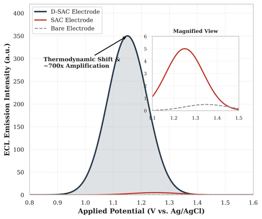
Figure 2. Electrochemiluminescence (ECL) Transduction Synergy. Applied potential vs. emission intensity curves reveal the massive thermodynamic shift and intensity amplification achieved by Dual-Atom Catalysts (D-SACs). By providing synergistic dual-site activation for coreactant pathways, D-SACs exhibit a nearly 700-fold signal enhancement relative to bare glassy carbon interfaces.
2.3. Atomically Precise Metal Nanoclusters
When metal atoms aggregate into clusters of specific "magic numbers" (e.g., Au25(SR)18), they transition from metallic conductors to semiconductor-like molecules.[4] These nanoclusters lack a continuous plasmon resonance and instead feature discrete Highest Occupied Molecular Orbital (HOMO) and Lowest Unoccupied Molecular Orbital (LUMO) gaps.
Transduction in nanoclusters is inherently optoelectronic. The discrete energy gap (Eg) is heavily dependent on the cluster core and ligand shell. When a target analyte (such as a heavy metal ion or biothiol) interacts with the protective thiolate ligands, it induces a charge-transfer perturbation or localized ligand exchange. This physically alters the Coulomb staircase charging and modulates the photoluminescence or ECL emission intensity directly, allowing for highly selective, label-free optical transduction.[4]
3. Interfacial Transduction in 2D Scaffolds
Two-dimensional (2D) materials, characterized by a high aspect ratio and atomic thickness, act as anisotropic platforms where surface termination chemistry, high conductivity, and specific topological sieving govern the transduction signal.
3.1. MXenes: Pseudocapacitive Gating and Metallic Cores
MXenes are a class of 2D transition metal carbides/nitrides (e.g., Ti3C2Tx) featuring a highly conductive metallic core flanked by tunable surface functional groups (-O, -OH, -F).[5] The primary transduction mechanism on MXenes involves field-effect gating and pseudocapacitive charge storage.
Because the surface terminations are highly electro-negative, they inherently pre-concentrate cationic targets and electrocatalytic biomarkers. However, pristine MXene sheets suffer from van der Waals-driven restacking, which drastically reduces the accessible electrochemically active surface area (ECSA). Modern sensors prevent this by intercalating ionic liquids or constructing 3D crumpled aerogels, which preserve the 2D conductive pathways while maximizing fluidic penetration.[5]
3.2. MOFs and COFs: Redox Hopping and Defect Engineering
Metal-Organic Frameworks (MOFs) and Covalent Organic Frameworks (COFs) offer precise, customizable porosity at the sub-nanometer scale, acting as flawless molecular sieves that physically exclude interfering matrix proteins.[6] However, pristine MOFs typically exhibit high inherent charge-transfer resistance (Rct), acting as insulators and stifling faradaic transduction.
To overcome this, MOFs are engineered to facilitate charge transfer via two mechanisms:
-
Redox Hopping: Charge is transported discretely between adjacent redox-active metal nodes (e.g., Cu, Co) through the organic linker framework.
-
π-π Quantum Tunneling: Introducing highly conjugated linkers allows for continuous π-π stacked pathways.[6]
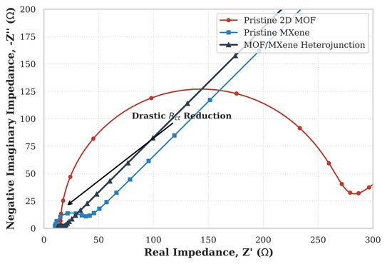
Figure 3. Interfacial Transduction Impedance. The Nyquist (EIS) plot demonstrates the fundamental limitation of pristine 2D MOFs (high Rct) and pristine MXenes (diffusion-limited capacitance). Hybridizing the two materials into a MOF/MXene heterojunction resolves both bottlenecks, achieving ultra-low interfacial resistance and seamless faradaic signal transduction.
Furthermore, integrating insulating MOFs with highly conductive MXene sheets creates a synergistic heterojunction. The MXene acts as a rapid electron highway, while the MOF provides topological selectivity and pre-concentration, dropping the overall Rct by orders of magnitude (as shown in Figure 3).
4. Mass Transport Transduction in 3D Hierarchical Architectures
The analytical sensitivity of any electrochemical sensor is ultimately bound by the laws of mass transport. In static solutions, planar electrodes suffer from rapid target depletion within the diffusion boundary layer.
4.1. Breaking the Cottrell Limit: Radial vs. Linear Diffusion
For a macroscopic planar electrode, the current response to a potential step is governed by semi-infinite linear diffusion, famously described by the Cottrell equation:
$$I(t) = \frac{n F A c_0 \sqrt{D}}{\sqrt{\pi t}}$$
where n is the number of electrons transferred, F is the Faraday constant, A is the area, c0 is the bulk concentration, D is the diffusion coefficient, and t is time. Because the current decays proportionally to t-1/2, steady-state sensing is impossible without external stirring.[7]
Three-dimensional (3D) hierarchical architectures (such as laser-induced graphene arrays, porous aerogels, or nano-pillar forests) bypass this limitation by restructuring the local fluidic environment. At the nanoscale tips and edges of 3D features, the diffusion field transitions from linear to convergent radial diffusion. For a hemispherical nano-feature of radius r, the steady-state faradaic current becomes time-independent:
$$I_{ss} = 2 \pi n F c_0 D r$$
This shift massively enhances the mass flux of the analyte to the transducer surface, allowing the sensor to maintain continuous, high-intensity signal generation without boundary-layer depletion.[7]
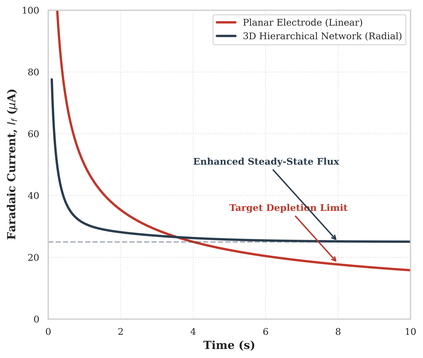
Figure 4. Mass Transport Kinetics. A simulated chronoamperometry plot comparing diffusion modes. Planar electrodes inevitably succumb to Cottrellian linear diffusion decay (t-1/2). In contrast, 3D hierarchical networks transition to convergent radial diffusion, establishing a non-zero, steady-state faradaic flux critical for continuous, real-time biosensing.
4.2. Directional Fluidics and Viscous Environments
Beyond altering the diffusion field geometry, 3D architectures physically manipulate the fluid matrix. In wearable sweat sensors or interstitial fluid monitors, sample volumes are miniscule (nanoliters) and highly viscous. Bio-inspired 3D electrospun fibers (e.g., Fermat helix structures) introduce capillary directional fluidics. By wicking the analyte aggressively toward the electroactive interface, these structures decouple the sensor's analytical response from the physiological flow rate of the patient, ensuring stable transduction regardless of external fluid dynamics.
5. Governing Transduction Modalities
The structural engineering detailed above culminates in three primary modes of electroanalytical signal conversion.
5.1. Faradaic Amperometry and Voltammetry
The most common transduction mechanism, relying on the direct oxidation or reduction of the target analyte at the electrode. The magnitude of the current is directly proportional to the analyte concentration, while the specific potential (E1/2) at which the reaction occurs provides qualitative identification. Nanostructuring improves this modality by lowering the activation energy barrier, shifting the requisite overpotential to near-zero values, and minimizing background interference from off-target oxidations (e.g., ascorbic acid or uric acid in physiological fluids).
5.2. Electrochemiluminescence (ECL)
ECL transduction couples electrochemical stimulus with optical emission. An applied voltage generates highly reactive, oxidized/reduced radical species at the electrode surface, which subsequently undergo a highly exergonic electron-transfer annihilation in the bulk solution. This reaction generates an excited state luminophore (e.g., [Ru(bpy)32+]*) that relaxes to the ground state by emitting a photon (hν).[8] Because the optical signal is decoupled from the electrical excitation, ECL possesses near-zero optical background noise, offering superior signal-to-noise ratios compared to standard photoluminescence.
5.3. Photoelectrochemistry (PEC)
PEC transduction is the inverse of ECL; it utilizes light to generate an electrical signal. A semiconductor nanostructure (e.g., TiO2 or CdS) absorbs incident photons with energy greater than its bandgap, generating electron-hole pairs (e-/h+).[9] The application of a bias potential, combined with strategically designed heterojunction band alignments (e.g., Z-scheme or Type-II junctions), spatially separates the charges, driving them toward the electrode and the electrolyte, respectively. The target biological analyte (e.g., a biomarker or cell) acts as a sacrificial electron donor or acceptor, modulating the photocurrent. PEC is highly valued for spatial resolution and minimizing electrical background noise in complex matrices.
6. Methodological Standardization for Transduction Characterization
As the complexity of nanostructured sensors scales, the risk of misinterpreting electroanalytical data escalates. Rigorous standardization protocols must be enforced to accurately quantify the transduction mechanism.[10]
6.1. Capacitive Background Deconvolution
High-surface-area 2D and 3D architectures inherently generate massive capacitive, non-faradaic background currents (Ic = Cdlν, where Cdl is the double-layer capacitance and ν is the scan rate). True faradaic signals (If) must be mathematically decoupled from this background to prevent the artificial inflation of reported analytical sensitivity.
6.2. ECSA Normalization
Normalizing current densities against geometric electrode dimensions is functionally obsolete for nanostructured materials. Signals must be normalized against the Electrochemically Active Surface Area (ECSA) or the roughness factor (Rf), determined via underpotential deposition (e.g., Hupd) or cyclic voltammetry in the double-layer region.
6.3. Operando Verification
Nanocatalysts, particularly SACs, are thermodynamically driven to agglomerate under applied bias. Relying solely on ex situ pre- and post-characterization is insufficient. Dynamic active-site stability must be verified using operando characterization (e.g., operando X-ray Absorption Spectroscopy (XAS) or Surface-Enhanced Raman Spectroscopy (SERS)) to prove that the proposed transduction mechanism holds true during active sensor operation.
7. Conclusion
The evolution of electrochemical sensors from bulk planar electrodes to precision-engineered nanostructures represents a fundamental paradigm shift in analytical transduction. By manipulating material architecture at the sub-nanometer, 2D, and 3D levels, scientists can precisely tune electronic density of states, circumvent macro-scale mass transport limitations, and unlock highly sensitive optical and photo-driven modalities. From the isolated d-orbitals of single-atom catalysts to the radial diffusion fields of 3D hierarchical aerogels, these tailored transduction mechanisms are the key to achieving the parts-per-trillion sensitivities required for next-generation clinical diagnostics, environmental monitoring, and wearable biochemical integration. However, realizing this potential demands rigorous standardization in data reporting and a unified understanding of the quantum and transport physics governing the solid-liquid interface.
References
- Oladipo, A. A.; Gazi, M. Single-Atom to Hierarchical Nanostructures: How Structural Precision Governs Sensing Mechanisms.. Anal. Methods . 2026, 19, 1-35.
- Jiao, L.; Xu, W.; Wu, Y.; Yan, H.; Gu, W.; Du, D.; Lin, Y.; Wang, Y. Single-atom catalysts boost signal amplification for biosensing. Chemical Society Reviews. 2021, 50(2), 1111–1135.
- Jin, Z.; Zhu, C.; et al. Fe and Ni Dual-Atom Catalysts as High-Efficiency Coreaction Accelerators to Enhance the Electrochemiluminescence of the Carbon Dots/S₂O₈²⁻ System.. Analytical Chemistry. 2025,, 97(4), 2115–2123.
- Jin, R.; Zeng, C.; Zhou, M.; Chen, Y. Atomically precise colloidal metal nanoclusters and their applications.. Chemical Reviews. 2016, 116(18), 10346–10413..
- Anasori, B.; Lukatskaya, M. R.; Gogotsi, Y. 2D metal carbides and nitrides (MXenes) for energy storage.. Nature Reviews Materials. 2017, 2(2), 16098.
- Jiao, L.; Yan, H.; Zhou, X.; Gu, W.; Wu, Y.; Du, D.; Lin, Y. Metal–organic frameworks for electrochemical sensing.. Advanced Materials. 2019, 31(45), 1900171.
- Amatore, C.; Sella, C.; Thouin, L. Theory and Experiments of Transport at Channel Microband Electrodes under Laminar Flows.. Analytical Chemistry. 2007, 79(22), 8502–8510.
- Miao, W. Electrogenerated chemiluminescence and its biorelated applications.. Chemical Reviews. 2008, 108(7), 2506–2553..
- Zhao, W. W.; Xu, J. J.; Chen, H. Y. Photoelectrochemical bioanalysis: the state of the art.. Chemical Society Reviews . 2015, 44(20), 7297–7321.
- Wei, C.; Shen, M.; Zhou, X.; Mandler, D. Advanced nanostructured electrocatalysts for energy conversion and bio-sensing.. Nano Today. 2018, 22, 18–35.