You're using an outdated browser. Please upgrade to a modern browser for the best experience.
Submitted Successfully!
Thank you for your contribution! You can also upload a video entry or images related to this topic. For video creation, please contact our Academic Video Service.
Version Summary Created by Modification Content Size Created at Operation
1 Helmut Schift -- 1114 2025-11-25 10:00:57 |
2 Format Correct Abigail Zou Meta information modification 1114 2025-11-25 10:01:45 |

Video Upload Options

We provide professional Academic Video Service to translate complex research into visually appealing presentations. Would you like to try it?
Cite
If you have any further questions, please contact Encyclopedia Editorial Office.
Schift, H. Nanoimprint—Mo(o)re than Lithography. Encyclopedia. Available online: https://encyclopedia.pub/entry/59293 (accessed on 25 December 2025).
Schift H. Nanoimprint—Mo(o)re than Lithography. Encyclopedia. Available at: https://encyclopedia.pub/entry/59293. Accessed December 25, 2025.
Schift, Helmut. "Nanoimprint—Mo(o)re than Lithography" Encyclopedia, https://encyclopedia.pub/entry/59293 (accessed December 25, 2025).
Schift, H. (2025, November 25). Nanoimprint—Mo(o)re than Lithography. In Encyclopedia. https://encyclopedia.pub/entry/59293
Schift, Helmut. "Nanoimprint—Mo(o)re than Lithography." Encyclopedia. Web. 25 November, 2025.
Peer Reviewed
Nanoimprint—Mo(o)re than Lithography

Nanoimprint lithography (NIL) is a high-resolution parallel patterning method based on molding. It has proven resolution down to the nanometer range and can be scaled up for large areas and high throughput. Its main characteristic is that the surface pattern of a mold is imprinted on a material that is displaced locally by using the difference in hardness of the mold and the moldable material, thus replicating its surface topography. This can be achieved by shaping a thermoplastic film by heating and cooling (T-NIL) or a photosensitive resin followed by a curing process for hardening (UV-NIL). In lithography, the local thickness contrast of the thin molded film can be used as a masking layer to transfer the pattern onto the underlying substrate. Therefore, NIL will be an alternative in fields in which electron-beam lithography and photolithography do not provide sufficient resolution at reasonable throughput. Direct imprint enables applications where a modified functional surface is needed without pattern transfer. NIL is currently used for high-volume manufacturing in different applications, like patterned sapphire substrates, wire grid polarizers, photonic devices, lightguides for AR/VR devices, metalenses, and biosensors for DNA analysis, and is being tested for semiconductor integrated circuit chips.
nanoimprint lithography molding stamp next-generation lithography high-volume manufacturing
For current and future devices with functional nanostructured surfaces, high-resolution parallel patterning methods that offer cost-effective manufacturing are required. Nanoimprint lithography (NIL) is the most prominent of the new lithographic techniques. NIL imprints a template with a three-dimensional (3D) surface topography on a moldable material. This is achieved by direct mechanical contact and material displacement. It is different from electron- or photon-based lithography (PL) and therefore incurs no structural loss due to the (optical) proximity effect [1][2]. Yet NIL is similar enough to standard lithography to permit the use of the same manufacturing and technology base: it uses templates made by advanced lithography and silicon process technology, a thin polymer resist as a masking layer for pattern transfer into the underlying substrate by etching (subtractive patterning) or onto it by electroplating (additive patterning), and imprint tools which still have significant resemblance to mask aligners, photolithographic steppers, and anodic bonding tools. NIL is mostly related to lithography. Apart from this, process solutions which are more related to other kinds of shaping processes arise, for example, using the difference in hardness of a mold and a moldable material, such as thermal injection molding (TIM), roll-to-roll (R2R) processes, coining, and casting, with the aim to replicate a mold relief into the surface. The aim of this entry is to present NIL as a basic lithographical process being able to replace standard PL, where a resist layer is patterned by mechanical means instead of exposure and wet development, but also to show that functional materials (e.g., photo- or bio-active materials) can be directly patterned, leading to enhanced functionality of a surface. The chapters on NIL in Springer Handbook of Nanotechnology [3][4] give a good overview about the process chains needed for understanding. The development of NIL towards high-volume manufacturing (HVM), with a variety of references on state-of-the-art techniques and companies, can be found in the book CRC Microlithography—Science and Technology [5]. Newest developments are presented at the annual International Nanoimprint and Nanoprint Technology (NNT) conference, which, in 2025, is celebrating the 30th anniversary since the publication of the first paper by Stephen Chou’s group [6]. This entry is intended to provide basic information about the NIL process and its origins, relate to other processes, and give definitions that make it possible to distinguish process variants, without going into detail about processing issues and specific parameters that might vary.
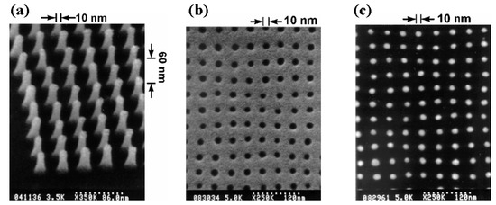
The historical start of NIL was at a time when the surface patterning of silicon wafers was performed using lithography with micrometer resolution. A molding-based lithography process using pattern transfer was demonstrated in the 1970s by Susumu Fujimori at NTT (Tokio, Japan, https://www.global.ntt/ (accessed on 7 July 2025)) in Japan [7], but it was not until 1995, when Stephen Chou and co-workers at the University of Minnesota, USA (later at Princeton University), published their first results, that it started to gain broader attention. They presented NIL as a new type of lithography by demonstrating 10 nm imprint capabilities at a time when 50 nm was considered the PL resolution limit [8][9]. At the same time, NIL, in its variant with UV-curable resists, was developed by Jan Haisma at Philips in Eindhoven, Netherlands [10]. In 2003 NIL was named one of the “10 emerging technologies that will change the world” [11]. NIL was considered revolutionary—and still is, due to three important distinctive characteristics (see Figure 1):
Figure 1. Micrographs showing the basic steps of NIL, demonstrated by S.Y. Chou. (a) NIL stamp in silicon with a 40 nm period array of pillars 60 nm in height, (b) imprinted 10 nm diameter holes in thin polymer film (PMMA), and (c) 10 nm metal dots after pattern transfer (lift-off), using thin polymer layer as a mask. Reprinted with permission from ref. [9]. Copyright 1997 American Vacuum Society.
  • It has a proven lateral resolution below 1 nm, which is far ahead of other, photon-based patterning techniques [12][13].
  • It imprints extremely thin polymer films, which result in residual layers of a few nm thickness and can be removed by anisotropic reactive ion etching [1].
  • It can imprint within micro-seconds and replicates multi-level and continuous structures in a variety of functional materials [14][15][16].
NIL is, therefore, considered both disruptive and evolutionary. It is disruptive because it uses the conformal contact of a stamp with a resist layer and displaces the material by squeeze flow and capillary action [11][12][13]. It, therefore, breaks the paradigm of non-contact in modern semiconductor integrated circuit (IC) chip HVM, which was possible by projecting photons and electrons onto a sensitive polymer film by optical means (e.g., lenses, mirrors, and shadow masks) and chemically modifying its solubility. At the same time NIL is evolutionary, because NIL profits from a variety of other technologies for low-cost applications, from large polymer films for packaging to optical versatile devices (OVDs) such as counterfeit tags for security, as well as for Compact Disc molding and micromanufacturing processes used in the so-called LiGA technique (German acronym for lithography, electroforming, and molding) [17][18][19][20]. In a historical context, it is a successor of the book-printing technique by Johannes Gutenberg, who, more than 550 years ago, made significant technological advances by inventing movable metallic letter types that could be copied by metal casting, employing wine presses as printing tools and inks that lasted for centuries. At the same time, it provided an unexpected and untypical solution for Gordon Moore’s law, which, since 1965, predicts the continuous demand for chips with a higher number of transistors and, today, is the driver of innovation in lithography. NIL came at a time when “nano” became the new paradigm of research.

References

  1. Heyderman, L.J.; Schift, H.; David, C.; Gobrecht, J.; Schweizer, T. Flow behaviour of thin polymer films used for hot embossing lithography. Microelectron. Eng. 2000, 54, 229–245.
  2. Schift, H. Nanoimprint lithography: An old story in modern times? A review. J. Vac. Sci. Technol. B 2008, 26, 458–480.
  3. Schift, H.; Kristensen, A. Nanoimprint lithography—Patterning resists using molding. In Handbook of Nanotechnology, 3rd ed.; Bhushan, B., Ed.; Springer: Berlin/Heidelberg, Germany, 2010; Chapter Part A/9; pp. 271–312. Available online: https://link.springer.com/chapter/10.1007/978-3-642-02525-9_9 (accessed on 7 July 2025).
  4. Schift, H.; Kristensen, A. Nanoimprint lithography—Patterning resists using molding. In Handbook of Nanotechnology, 4th ed.; Bhushan, B., Ed.; Springer: Berlin/Heidelberg, Germany, 2017; Chapter Part A/5; pp. 113–142.
  5. Resnick, D.; Schift, H. Nanoimprint lithography. In Microlithography—Science and Technology, 3rd ed.; Suzuki, K., Smith, B.W., Eds.; CRC Press: Boca Raton, FL, USA, 2020; Chapter 12; pp. 595–678.
  6. International Conference on Nanoimprint and Nanoprint (NNT). Available online: http://www.nntconf.org (accessed on 7 July 2025).
  7. Fujimori, S. Fine pattern fabrication by the molded mask method (nanoimprint lithography) in the 1970s. Jpn. J. Appl. Phys. 2009, 48, 06FH01.
  8. Chou, S.Y.; Kraus, P.R.; Renstrom, P.J. Imprint of sub-25 nm vias and trenches in polymers. Appl. Phys. Lett. 1995, 67, 3114–3116.
  9. Chou, S.Y.; Kraus, P.R.; Zhang, W.; Guo, L.; Zhuang, L. Sub-10 nm imprint lithography and applications. J. Vac. Sci. Technol. B 1997, 15, 2897–2903.
  10. Haisma, J.; Verheijen, M.; van den Heuvel, K.; van den Berg, J. Mold-assisted lithography: A process for reliable pattern replication. J. Vac. Sci. Technol. B 1996, 14, 4124–4128.
  11. Huang, G.T. 10 Emerging Technologies That Will Change the World. In MIT Technology Review; Technology Review Inc.: Cambridge, MA, USA, 2003; Available online: https://www.technologyreview.com/10-breakthrough-technologies/2003/ (accessed on 7 July 2025).
  12. Hua, F.; Sun, Y.; Gaur, A.; Meitl, M.A.; Bilhaut, L.; Rotkina, L.; Wang, J.; Geil, P.; Shim, M.; Rogers, J.A.; et al. Polymer imprint lithography with molecular-scale resolution. Nano Lett. 2004, 4, 2467–2471.
  13. Tan, G.; Nozawa, Y.; Funabasama, T.; Koyama, K.; Mita, M.; Kaneko, S.; Komura, M.; Matsuda, A.; Yoshimoto, M. Atomic-scale thermal behavior of nanoimprinted 0.3 nm high step patterns on PMMA polymer sheets. Polym. J. 2016, 48, 225–227.
  14. Chou, S.Y.; Keimel, C.; Gu, J. Ultrafast and direct imprint of nanostructures in silicon. Nature 2002, 417, 835–837.
  15. Tormen, M.; Sovernigo, E.; Pozzato, A.; Pianigiani, M.; Tormen, M. Sub-100 μs nanoimprint lithography at wafer scale. Microelectron. Eng. 2015, 141, 21–26.
  16. Schift, H. Nanoimprint lithography: 2D or not 2D? A review. Appl. Phys. A 2015, 121, 415–435.
  17. Becker, E.W.; Ehrfeld, W.; Hagmann, P.; Maner, A.; Münchmeyer, D. Fabrication of microstructures with high aspect ratios and great structural heights by synchrotron radiation lithography, galvanoforming and plastic molding (LIGA process). Microelectron. Eng. 1986, 4, 35–56.
  18. Gale, M.T. Replication techniques for diffractive optical elements. Microelectron. Eng. 1997, 34, 321–339.
  19. Schift, H.; David, C.; Gabriel, M.; Gobrecht, J.; Heyderman, L.J.; Kaiser, W.; Köppel, S.; Scandella, L. Nanoreplication in polymers using hot embossing and injection molding. Microelectron. Eng. 2000, 53, 171–174.
  20. Heckele, M.; Schomburg, W.K. Review on micro molding of thermoplastic polymers. J. Micromech. Microeng. 2004, 14, R1–R14.
More
Upload a video for this entry
Information
Contributor MDPI registered users' name will be linked to their SciProfiles pages. To register with us, please refer to https://encyclopedia.pub/register : Helmut Schift
View Times: 18
Online Date: 25 Nov 2025
Notice
You are not a member of the advisory board for this topic. If you want to update advisory board member profile, please contact office@encyclopedia.pub.
OK
Confirm
Only members of the Encyclopedia advisory board for this topic are allowed to note entries. Would you like to become an advisory board member of the Encyclopedia?
Yes
No
${ textCharacter }/${ maxCharacter }
Submit
Cancel
There is no comment~
${ textCharacter }/${ maxCharacter }
Submit
Cancel
${ selectedItem.replyTextCharacter }/${ selectedItem.replyMaxCharacter }
Submit
Cancel
Confirm
Are you sure to Delete?
Yes No
Academic Video Service