1. Silicon-Based Solar Cells
1.1. Historical Context and Enduring Relevance
Silicon-based solar cells have not only been the cornerstone of the photovoltaic industry for decades but also a symbol of the relentless pursuit of renewable energy sources. The journey began in 1954 with the development of the first practical silicon solar cell at Bell Labs, marking a pivotal moment in the history of solar energy
[1]. This invention, achieving an efficiency of about 6%, was a significant leap from earlier solar energy attempts, which were largely inefficient and impractical for widespread use
[1].
The dominance of silicon in the photovoltaic market can be attributed to several key factors. Firstly, silicon is the second most abundant element in the Earth’s crust, making it readily available for solar cell production
[2]. This abundance has been a critical factor in the widespread adoption and scalability of silicon-based solar cells. Secondly, the semiconductor properties of silicon make it an ideal material for converting sunlight into electricity. Its bandgap is well suited for absorbing a broad range of the solar spectrum, thereby maximizing the energy conversion efficiency
[2].
Over the years, the manufacturing processes for silicon solar cells have undergone significant evolution, transitioning from simple p-n junctions to more complex designs that enhance light absorption and minimize energy losses
[3]. The development of crystalline silicon technology, both in monocrystalline and polycrystalline forms, has been central to this evolution. Monocrystalline silicon cells, known for their higher efficiency due to their uniform crystalline structure, have become increasingly popular in high-performance applications
[3]. On the other hand, polycrystalline silicon cells, made from multiple silicon crystals, offer a more cost-effective solution, albeit with slightly lower efficiency
[3].
The 1970s and 1980s were marked by significant milestones in the development of silicon-based solar cells, with the introduction of new technologies such as surface passivation and antireflective coatings
[4]. These innovations were crucial in enhancing the efficiency and durability of silicon solar cells, propelling them to the forefront of solar energy solutions. By the late 20th century, silicon solar cells had firmly established themselves as the standard in the photovoltaic industry, with efficiencies surpassing 15%
[4].
In the 21st century, the focus shifted towards further improving the efficiency and reducing the cost of silicon solar cells. The introduction of PERC (passivated emitter and rear cell) technology and the development of bifacial solar cells are examples of innovations that have significantly boosted the performance of silicon-based solar cells
[5]. These advancements have not only improved efficiency but also extended the lifespan of solar panels, making them more appealing for both residential and commercial applications
[5].
1.2. Recent Innovations in Crystalline Silicon Structures
Regarding crystalline silicon (c-Si) solar cells, recent years have been marked by groundbreaking innovations aimed at transcending the traditional efficiency limits. These advancements are pivotal in sustaining silicon’s competitiveness in the rapidly evolving photovoltaic market. A notable example is the work by Zhang et al.
[6], which delves into the realm of perovskite/crystalline silicon tandem solar cells. Their research systematically reviews the latest progress in this area, focusing on the structure of perovskite top cells, intermediate interconnection layers, and crystalline silicon bottom cells. They emphasize the importance of optical and electrical engineering in each layer, highlighting how these aspects are integral throughout the device preparation process. This study is significant, as it demonstrates the potential of tandem cells to achieve efficiencies above 30%, a remarkable feat in solar cell technology
[6].
Another significant contribution comes from Singh et al.
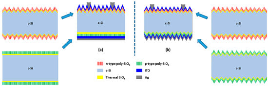
[7] and presents the creation of c-Si bottom cells using high-temperature polycrystalline-SiOx (poly-SiOx) carrier-selective passivating contacts (CSPCs), a promising approach for high-efficiency tandem cells (see
Figure 1). The research involved tuning ultra-thin SiOx layers and optimizing the passivation of both p-type and n-type doped poly-SiOx CSPCs, with a focus on p-type doped poly-SiOx CSPCs on textured interfaces through a two-step annealing process. The integration of these optimized bottom cells into four-terminal (4T) and two-terminal (2T) tandem structures led to a conversion efficiency of 28.1% and 23.2%, respectively.
Figure 1. (
a) A single-sided textured (SST) poly-SiOx passivated crystalline silicon (c-Si) solar cell, featuring symmetric n-type doped poly-SiOx on a double-sided textured (DST) substrate at the top and symmetric p-type doped poly-SiOx on a double-sided polished (DSP) substrate at the bottom; (
b) a DST poly-SiOx passivated c-Si solar cell, equipped with symmetric n-type doped poly-SiOx on the top and symmetric p-type doped poly-SiOx, both situated on DST substrates. “ITO” refers to indium tin oxide. Reprinted with permission from ref.
[7], copyright 2023, Progress in Photovoltaics: Research and Applications.
Furthering the innovation in thin crystalline silicon solar cells, the study by Xie et al.
[8] reported significant advancements in the efficiency of thin crystalline silicon (c-Si) solar cells, a promising alternative to the traditional, thicker c-Si solar cells, due to their cost-effectiveness and enhanced flexibility. Their approach involved the implementation of advanced cell design optimizations, focusing on a prototype with a thickness of 20 μm. The results of their optimizations are notable: the short-circuit current density increased from 34.3 mA/cm
2 to 38.2 mA/cm
2, the open-circuit voltage improved from 632 mV to 684 mV, and the fill factor exhibited an enhancement from 76.2% to 80.8%. These improvements collectively resulted in a significant absolute efficiency increase of 4.6%, elevating the overall efficiency from 16.5% to 21.1%. The experimental outcomes were corroborated by device simulations, providing a comprehensive understanding of the efficiency enhancements that can be achieved through optimized design strategies.
Additionally, the work by Yamamoto et al.
[9] presents a 29.2% power conversion efficiency in a two-terminal (2T) perovskite/crystalline Si hetero-junction tandem solar cell, using a 145 μm thick industrial Czochralski (CZ) Si wafer. This achievement, a notable advancement in 2T tandem solar cell technology, is primarily due to structural optimizations like improved surface passivation of the perovskite layer and advanced light management techniques. Addressing the industrial application challenges, the authors also explored the potential of four-terminal (4T) tandem solar cells as a viable alternative. Drawing on their foundational technologies, which have already achieved a 22.2% efficient perovskite single-junction solar cell module and a 26% efficient hetero-junction back contact solar cell, they demonstrated the feasibility of achieving an around 30% conversion efficiency in 4T perovskite/hetero-junction crystalline Si tandem solar cells, with a significantly reduced cell size of approximately 64 cm
2.
1.3. Efficiency and Commercial Viability Analysis
The efficiency of silicon-based solar cells has seen a remarkable increase over the years, with commercial monocrystalline silicon solar cells now achieving efficiencies of over 20%
[10]. This improvement is largely attributed to the incorporation of advanced materials and innovative cell designs. A significant contribution to this advancement is the widespread adoption of passivated emitter and rear cell (PERC) technology, which offers higher efficiency and lower production costs compared to traditional c-Si cells
[10].
J. Müller’s work
[10] highlights the significant improvements in cost reduction and conversion efficiency increase that have been achieved in large-scale industrial production over the last decade. This progress has made photovoltaics (PVs) cost-competitive with other electricity generation methods. Müller discusses the key concepts and methods based on Hanwha Q CELLS’ experience, including the fast transfer of cell technologies from laboratory to production and accelerated progress in cell efficiency, quality, and reliability. The study notes that the cell conversion efficiency has increased by 0.5% abs per year, with average cell conversion efficiencies exceeding 20% using boron-doped p-type multicrystalline (mc-Si) substrates and 22% using Czochralski-grown silicon (Cz-Si) substrates
[10].
In an effort to reduce the cost of photovoltaic (PV) power generation, Irie and group
[11] focused on three primary objectives: lowering the manufacturing costs of PV modules, improving the efficiencies of cells and modules, and extending the long-term output power warranty of PV modules. They developed a high-quality and cost-effective seed-cast wafer, which achieved an efficiency of 20.54% with passivated emitter and rear cells (PERCs). Additionally, the authors addressed module longevity concerns by identifying and mitigating key degradation modes, including ohmic contact degradation and potential induced degradation (PID). To assess the durability of their modules under real-world conditions, they conducted extensive stress tests, simulating environments with ultraviolet light, heat, humidity, and electrical potential differences. These tests, including those on field-aged modules, demonstrated that their technology can ensure a module lifetime exceeding 30 years, with resistance to PID, particularly in the context of Japanese domestic environments, marking a significant advancement in PV module technology.
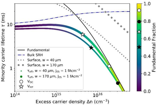
Augusto and colleagues
[12] reported significant advancements in silicon solar cell technologies, with several technologies now surpassing or nearing 26% efficiency. This progress is largely due to the integration of dielectric and amorphous silicon-based passivation layers and the reduction in metal/silicon contact areas, leading to surface saturation current densities below 3 fA cm⁻
2 (see
Figure 2). They found that in passivated contact solar cells, the majority of the recombination at open circuit is due to fundamental processes like Auger and radiative recombination, accounting for over three-quarters of the total recombination. However, this fraction decreases significantly at the maximum power point, where surface and bulk Shockley–Read–Hall recombination mechanisms become prevalent. Their study emphasizes the importance of reducing bulk recombination and enhancing surface passivation to improve solar cell performance under operational conditions. The authors demonstrated that thinner wafers and lower surface saturation current densities below 1 fA cm⁻
2 are crucial for increasing the practical efficiency limit by up to 0.6% absolute. For high-quality n-type bulk silicon with a minority carrier lifetime of 10 ms, they identified an optimal wafer thickness range of 40–60 μm, which was significantly different to the previously assumed 110 μm. Within this thickness range, achieving surface saturation current densities near 0.1 fA cm⁻
2 is essential to approach the fundamental efficiency limit. Experimentally, they have achieved surface saturation currents below 0.5 fA cm⁻
2 on pi/CZ/in structures across a range of wafer thicknesses (35–170 μm), indicating the potential to attain open-circuit voltages close to 770 mV and bandgap–voltage offsets near 350 mV. Finally, the authors suggest using the bandgap–voltage offset as a comparative metric for evaluating the quality of high-performing experimental solar cells across various commercially relevant photovoltaic cell absorbers and architectures.
Figure 2. Model for the effective minority carrier lifetime in structures using n-type wafers of thicknesses of 170 μm and 40 μm. These wafers are characterized by a bulk Shockley–Read–Hall (SRH) lifetime of 10 ms, a bulk resistivity of 3.55 Ω cm (equivalent to a dopant concentration of 1.3 × 10
15 cm⁻
3), and a combined surface recombination velocity (J0S) of 1 fAcm⁻
2 from both surfaces. In the accompanying plots, various curves are used to distinguish between different recombination mechanisms. A color bar is included to denote the proportion of fundamental recombination, which encompasses both Auger and radiative processes. The black star represents the maximum voltage at a close circuit, whereas the black circle represents the power voltage at a close circuit. The generation current for these wafers is determined based on the appropriate Lambertian light trapping limit for each specific thickness. Additionally, markers within the color bar highlight the proportions of fundamental recombination at the points of maximum power and during open-circuit injections. Reprinted with permission from ref.
[12], copyright 2020, Journal of Materials Chemistry A.
Mao’s research
[13] explores the dominance and evolution of crystalline silicon solar cells in the photovoltaic market, focusing on the transition from polycrystalline to more cost-effective monocrystalline silicon cells, which is driven by advancements in silicon materials and wafer technologies. The study highlights the increasing conversion efficiency of monocrystalline cells, particularly through high-efficiency technologies like passivated emitter and rear cells (PERCs). They analyzed and forecast the future of solar cell industrialization, concluding that N-type tunnel oxide passivated contact (TOPCon) solar cell technology is poised to become the next mainstream technology after PERC. Additionally, the authors identified interdigitated back contact (IBC) structures and selective all-passive contact technologies as viable paths to achieving high-efficiency solar cells. This synthesis of efficiency, cost, and technological compatibility underlines the potential for the industrialization of cost-effective, high-efficiency monocrystalline silicon solar cells.
In terms of commercial viability, silicon solar cells continue to benefit from economies of scale and well-established supply chains. The cost of silicon PV cells has decreased significantly, making solar energy more competitive with traditional energy sources. However, the market also faces challenges such as the need for more sustainable manufacturing processes and the management of end-of-life solar panels.
1.4. Challenges and Future Outlook
Despite their success, silicon-based solar cells face several challenges. One of the primary challenges is the nearing of the theoretical efficiency limit for single-junction silicon cells
[14]. This limitation has necessitated the exploration of new designs, such as tandem cells. Rong et al.
[14] review the progress in perovskite solar cells (PSCs), which are increasingly being considered for tandem applications with silicon cells. They note that PSCs have achieved lab-scale power conversion efficiencies of 23.3%, rivaling commercial multicrystalline silicon solar cells. However, stability and upscaling for mass production remain critical concerns for the commercialization of PSCs
[14].
Environmental concerns associated with the production and disposal of silicon PV cells are also significant challenges. Lunardi et al.
[15] examined the expanding role of solar photovoltaics (PVs) as a sustainable and low-carbon electricity source, focusing on a life cycle assessment (LCA) of current and emerging solar cell technologies, predominantly silicon wafer cells and prospective silicon/thin-film tandem devices. They demonstrated that efficiency enhancements, especially through the integration of atomic hydrogen in silicon wafers, offer significant environmental benefits, justifying the additional required inputs. The study also underscores the importance of top-cell material stability in tandem solar cells to prolong the lifespan of the underlying silicon bottom cell. Addressing the end-of-life scenario for PV modules, traditionally destined for landfills, the authors highlight the urgent need for sustainable recycling practices in light of the rapid global adoption of photovoltaics. Despite challenges in the environmentally and financially viable dismantling of PV modules, their research is directed towards developing effective recycling methods, including chemical, thermal, and mechanical techniques, to optimize material recovery and foster sustainable industry practices.
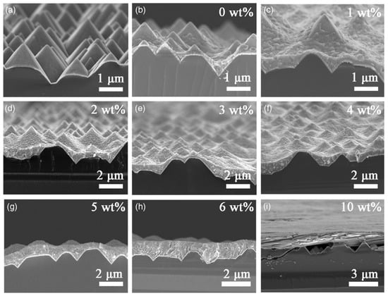
Wang et al.
[16] introduce a simple solvent engineering technique involving the use of starch additive in a MAPbI3-based one-step spin-coating process at room temperature, aimed at efficiently depositing perovskite on textured silicon surfaces for perovskite/Si monolithic tandem solar cells (TSCs) (see
Figure 3). The authors investigate the influence of different starch concentrations on the morphological, structural, optical, and photovoltaic properties of the perovskite films. The results show that starch improved the solution viscosity and formed hydrogen bonds with CH
3NH
3⁺, facilitating the formation of perovskite films with a crystal structure that is compatible with textured silicon surfaces. A concentration of 5 wt% starch enables complete coverage of textured silicon surfaces with an average film thickness of around 600 nm. This approach not only stabilizes the crystal structure and device performance of the perovskite film and the planar solar cell but also locks water molecules at the perovskite grain boundaries due to the presence of starch. Their findings demonstrated the potential of this method in achieving uniform light absorption in perovskite layers and a well-matched current density in perovskite/Si monolithic TSCs, with a best calculated cell efficiency exceeding 29%.
Figure 3. Cross-sectional scanning electron microscopy (SEM) images illustrating (
a) a silicon surface textured with pure pyramids and (
b–
i) the same pyramid-textured silicon surface overlaid with perovskite films, each with varying starch ratios. These ratios include (
b) 0 wt%, (
c) 1 wt%, (
d) 2 wt%, (
e) 3 wt%, (
f) 4 wt%, (
g) 5 wt%, (
h) 6 wt%, and (
i) 10 wt%. Reprinted with permission from ref.
[16], copyright 2020, Energy Technology.
Zhao et al.
[17] provide a detailed exploration of recent advances in photovoltaic technologies, specifically focusing on organic and perovskite-based solar cells. The authors explore the intricacies of crystallization mechanisms in these cells, underlining their crucial role in influencing cells’ efficiency and performance. Their work also addresses the pivotal challenge of material stability, highlighting innovative approaches in charging materials to boost solar cell efficiency and durability. Additionally, it explores the commercial potential of these technologies, emphasizing scalable fabrication techniques and the promising capabilities of tandem solar cells, which are capable of exceeding the traditional Shockley–Queisser limit, thus heralding a new era in solar energy technology.
The future outlook for silicon-based solar cells is promising, with ongoing research focused on enhancing their efficiency and reducing costs. Innovations such as the integration of perovskite layers with silicon to create tandem cells, and the use of nanotechnology for light management, are expected to play a significant role in the next generation of silicon PV cells. Moreover, the industry is moving towards more sustainable practices, including the use of greener materials and the development of efficient recycling methods for solar panel components.
2. Gallium Arsenide (GaAs)
Gallium arsenide (GaAs) solar cells are among the highest efficiency solar cells available today. Unlike silicon-based solar cells, GaAs cells can convert more of the solar spectrum into electricity
[18]. This is primarily due to the direct bandgap of GaAs, which allows for efficient absorption of sunlight and its conversion into electrical energy
[18]. The highest efficiency of GaAs solar cells has surpassed 29%, a benchmark set in controlled laboratory conditions
[18]. This high efficiency is attributed to the material’s ability to operate effectively at higher temperatures and its superior response to low-light conditions compared to silicon cells.
The unique properties of GaAs solar cells make them particularly suitable for space applications. Their high efficiency, coupled with a resistance to radiation, ensures long-term operation in the harsh environment of space
[19]. NASA has utilized GaAs solar cells in various missions, appreciating their reliability and superior performance
[19]. Furthermore, in concentrated photovoltaic (CPV) systems, GaAs solar cells are used to harness sunlight that is concentrated onto the cells by lenses or mirrors. This application benefits from the high efficiency of GaAs cells under intense light conditions, making them ideal for CPV installations where space is at a premium and maximum power output is desired
[20]. Schön and group
[21] present the development of thin, lightweight, flexible solar cells with an epitaxy thickness of about 10 μm, utilizing an inverted metamorphic triple-junction structure with Ga
0.51In
0.49P/GaAs/Ga
0.73In
0.27As subcells. Optimized for end-of-life (EOL) efficiency post 1 MeV electron irradiation, the cells demonstrated a predicted efficiency potential of 30.9% under AM0 illumination before irradiation and 26.7% after. The tested cells achieved an up to 30.2% conversion efficiency pre-irradiation and 25.4% post-irradiation, with a remarkable power-to-mass ratio reaching 3.0 W/g, marking significant advancements in solar cell technology. Additionally, the solar cells showed exceptional mechanical stability, with no performance degradation after rigorous temperature cycling, highlighting their potential for space applications.
Despite their advantages, GaAs solar cells face significant challenges that limit their widespread adoption
[22]. The primary issue is their cost of production. Gallium and arsenic, the core materials in GaAs cells, are expensive and less abundant than silicon, leading to higher manufacturing costs. The complex manufacturing process of GaAs cells, which requires high-purity materials and sophisticated fabrication techniques, further escalates the cost
[22]. Material scarcity is another concern
[23]. Gallium is a byproduct of the smelting of other metals, notably aluminum and zinc, and its availability is dependent on the production levels of these metals. Arsenic, while more abundant, poses environmental and health risks during extraction and processing, necessitating stringent handling and disposal measures
[23].
Efforts are underway to address the cost and material scarcity challenges faced by GaAs solar cells. Innovations in manufacturing techniques, such as the development of thin-film GaAs solar cells, aim to reduce the material usage and production costs
[24]. Thin-film technologies allow for the deposition of GaAs layers on inexpensive substrates, significantly lowering the amount of gallium and arsenic that is required
[24].
Recycling of gallium from electronic waste is another avenue being explored to mitigate material scarcity. As the demand for electronics continues to grow, so does the potential for recycling gallium, providing a more sustainable source for the production of GaAs solar cells
[25]. Ndalloka et al.
[26] explain that GaAs solar cells, known for their direct bandgap and high efficiencies of up to 28.8% for single-junction and 42.3% for triple-junction cells, are crucial in space and to achieve concentrated PV power generation due to their durability and thermal stability. Despite their efficiency, production sees nearly 85% of GaAs wasted, highlighting the need for advanced recycling methods. Techniques like nitrogen pyrolysis have achieved material reduction rates of up to 98.2% for EVA and 98.69% for PET. The authors further explain that experiments have shown stable gallium and arsenic recovery rates, with vacuum metallurgy providing a recovery efficiency of 93.48%. However, recycling can affect performance, indicating that the balance between sustainability and maintaining high efficiency is complex, yet essential, for future advancements.
3. Cadmium Telluride (CdTe)
Cadmium Telluride (CdTe) has emerged as a prominent semiconductor material in the field of thin-film solar cells. Characterized by its direct bandgap and high absorption coefficient, CdTe allows for the production of cells that are not only thinner but also more efficient in converting sunlight to electricity compared to traditional silicon-based cells
[27]. This material has been at the center of significant research and development efforts, aiming to leverage its properties to create cost-effective, efficient, and scalable solar energy solutions. The use of CdTe in thin-film solar cells represents a pivotal advancement in photovoltaic technology, offering a promising pathway to achieving higher efficiency and lower production costs in solar energy systems
[28].
The integration of CdTe into photovoltaic cells underscores the importance of material science in the ongoing evolution of solar energy technologies. As researchers continue to explore and refine the properties of semiconductor materials like CdTe, the potential for further enhancements in solar cell efficiency and the broader adoption of solar energy becomes increasingly tangible. This pursuit not only addresses the technical and economic challenges associated with solar energy but also contributes to the global effort to transition towards more sustainable and environmentally friendly energy sources
[29].
Cadmium Telluride (CdTe) is distinguished by its high absorption coefficient, which enables it to absorb sunlight more efficiently than many other semiconductor materials
[30]. This property allows CdTe solar cells to be manufactured with significantly thinner photovoltaic layers, without compromising their ability to capture solar energy. The thickness of a CdTe layer in a solar cell is typically less than 10 μm, which is considerably thinner than the silicon layers used in traditional photovoltaic cells, which can be over 200 μm thick
[30]. This efficient use of material not only reduces the amount of raw material needed but also contributes to the overall efficiency of the solar cells by minimizing electron loss
[31].
The production of CdTe solar cells is characterized by its cost-effectiveness, attributed to the simplicity of the manufacturing process and the low material usage
[32]. The process for creating CdTe cells involves depositing a thin layer of CdTe material onto a glass or flexible substrate, which can be carried out at relatively low temperatures and with less energy compared to the production of silicon cells. This streamlined manufacturing process, coupled with the reduced material requirements, results in lower production costs, making CdTe solar cells a more affordable option for large-scale deployment
[32]. The economic advantages of CdTe technology have been instrumental in its adoption and growth within the solar energy market
[33].
The energy payback time (EPT) of CdTe solar cells is among the shortest for photovoltaic technologies
[34]. EPT refers to the amount of time that a solar cell takes to generate the amount of energy that was used to produce it. Studies
[34][35] have shown that CdTe solar cells have an EPT of less than one year, which is significantly lower than that of many silicon-based solar cells. This short EPT underscores the environmental friendliness of CdTe solar cells, as they quickly offset the energy consumed during their production, leading to a net positive energy generation over their lifespan
[35].
CdTe solar cells exhibit superior performance across a wide range of temperatures and under low-light conditions
[36]. Unlike some other photovoltaic materials, whose efficiency significantly drops at high temperatures, CdTe solar cells maintain a relatively stable output even in hot climates. Additionally, CdTe cells are effective at converting diffuse sunlight into electricity, which makes them particularly suitable for regions with frequent cloud cover or haze. This versatility enhances the applicability of CdTe solar cells in diverse geographical locations, contributing to their growing popularity in the global solar energy market
[36].
One of the primary concerns associated with CdTe solar cells is the toxicity of cadmium, a heavy metal that is used in their production. Cadmium is recognized for its potential to harm human health and the environment if not properly managed
[37]. The use of cadmium in consumer products, including photovoltaic cells, has raised questions about the long-term implications of CdTe solar cell disposal and the risk of cadmium release into the environment. However, industry practices have evolved to include rigorous safety standards and recycling programs aimed at mitigating these risks. Research into encapsulation and recycling technologies continues to minimize the environmental impact of cadmium in CdTe solar cells
[37].
The limited availability of tellurium, a key component in CdTe solar cells, poses a challenge to the scalability of this technology
[38]. Tellurium is one of the least abundant elements in the Earth’s crust, and its supply is predominantly derived as a byproduct of copper refining
[38]. The scarcity of tellurium could limit the potential for significant expansion of CdTe solar cell production, prompting research into more abundant alternative materials or more efficient recycling methods to ensure the sustainable growth of CdTe photovoltaics
[38].
The recycling and disposal of CdTe solar cells present challenges due to the need for specialized processes to safely handle and recover materials, particularly cadmium. While recycling programs have been developed to address these challenges, ensuring the safe and efficient recycling of CdTe solar cells at the end of their lifecycle is critical to minimizing their environmental impact
[39]. Advances in recycling technologies and strategies are essential to support the sustainable deployment of CdTe solar cells, with ongoing research focused on improving the efficiency and accessibility of recycling processes
[39].
Recent breakthroughs in the efficiency of Cadmium Telluride (CdTe) solar cells have been significant, with researchers achieving record cell efficiencies through advancements in junction quality and back contact improvements
[40]. Innovations such as the development of high-resistivity transparent layers and the optimization of the CdTe/CdS junction have led to enhanced light absorption and reduced recombination losses, pushing CdTe cell efficiencies closer to their theoretical limits
[40]. Additionally, the introduction of new back contact materials has improved the collection of carriers, further increasing the efficiency of CdTe solar cells
[41]. These advancements not only enhance the performance of CdTe solar cells but also contribute to reducing the cost per watt of solar electricity, making solar energy more competitive with traditional energy sources. Alfadhili and group
[42] explored the impact of methylammonium iodide treatment on developing a Te layer atop CdTe and ZnTe films for creating back contacts in CdTe solar devices. The authors developed eight different back contact designs to assess whether Te or ZnTe would enhance the device’s performance. Alongside performance metrics, the group measured barrier heights to better understand the back contact energetics. Their findings showed that incorporating Te or ZnTe as back contacts significantly improves VOC and device efficiency by optimizing band alignment.
Research into alternative materials and doping strategies aims to reduce the toxicity and improve the efficiency of CdTe solar cells. Efforts to replace or reduce the use of cadmium with less toxic materials without compromising cell performance are underway. For instance, the exploration of alternative buffer layers to replace the standard cadmium sulfide (CdS) layer with materials that have similar electronic properties but a lower environmental impact is a focus of current research
[43]. Doping strategies involving the introduction of specific elements into the CdTe layer have been shown to enhance the material’s electrical properties, leading to improved cell efficiencies
[44]. These advancements in material science not only address environmental concerns but also open new pathways for the development of high-efficiency, low-impact solar cells. Al-Kuhaili et al.
[45] doped CdTe To overcome these concerns; samarium, a rare-earth metal known for its superior conductivity and high valence, was used for extrinsic doping. This study involved depositing samarium-doped CdTe thin films, with samarium concentrations ranging from 0 to 6.2 at%. The post-doping results showed a remarkable transformation in the films’ photoelectric properties, including a switch from p-type to n-type, an eightfold decrease in resistivity to 7.6 × 10
−2 Ω⋅cm, successful ohmic contact formation, and a reduced optical bandgap that improved the solar absorption.
Innovations in manufacturing processes have played a crucial role in reducing the costs and improving the scalability of CdTe solar cell production. Advances in deposition techniques, such as close-spaced sublimation (CSS) and vapor transport deposition (VTD), have improved the uniformity and quality of CdTe layers while reducing production times and material waste
[46]. The development of scalable manufacturing solutions, including roll-to-roll processing for flexible solar cells, has the potential to significantly lower production costs and expand the applicability of CdTe technology to a wider range of surfaces and applications
[47]. These manufacturing innovations not only enhance the economic viability of CdTe solar cells but also contribute to the sustainability of solar energy as a scalable renewable resource. Siegler and group
[48] explored the hurdles impacting the development of perovskite–CdTe tandem photovoltaics (PVs) and presented future directions for this structure. The authors crafted PVs with a wide-bandgap CH
3NH
3PbBr
3 (MAPBr) as the top absorber layer, noting reasonable efficiency but encountering significant optical haze that restricted the CdTe layer’s light absorption and the tandem cell’s performance. Utilizing SCAPS software, the researchers simulated a four-terminal (4T) MAPBr-CdTe tandem setup, assessing the permissible haze level in the perovskite layer to enhance the efficiency compared with single-junction CdTe cells.
The ongoing challenge of increasing the conversion efficiency of CdTe solar cells to compete with silicon-based cells remains a key focus of research and development. While recent advancements have significantly improved CdTe cell efficiencies, reaching and surpassing the efficiency levels of silicon-based solar cells requires continuous innovation in material properties, cell design, and manufacturing processes
[49]. Efforts to understand and mitigate efficiency losses due to defects, grain boundaries, and interface recombination are critical to further advancements in CdTe solar cell technology
[50].
CdTe solar cells face market challenges, including the public perception of cadmium’s toxicity and competition with other types of solar cells
[51]. Addressing these challenges requires ongoing efforts to educate the public and stakeholders about the safety measures and environmental benefits of CdTe technology, as well as the competitive advantages of CdTe solar cells in terms of cost, efficiency, and versatility
[51]. Overcoming market adoption barriers is essential to fully realizing the potential of CdTe solar cells in the global renewable energy landscape.
4. Copper Indium Gallium Selenide (CIGS)
Copper indium gallium selenide (CIGS) stands out within the thin-film category for its exceptional photovoltaic properties and potential for high-efficiency solar cells
[52]. CIGS is a tetrahedrally bonded semiconductor with a chalcopyrite structure, which is key to its desirable photovoltaic characteristics. The material’s composition can be finely tuned to optimize its absorption spectrum, making it highly efficient at converting sunlight into electrical energy. This adaptability, combined with the material’s ability to be deposited on flexible substrates, positions CIGS solar cells as a versatile solution for a wide range of solar energy applications
[53].
CIGS solar cells are distinguished by their high absorption coefficient and direct bandgap, which enable them to efficiently absorb sunlight and convert it into electricity
[54]. The direct bandgap of CIGS can be adjusted to between 1.0 and 1.7 eV, allowing for optimal absorption of the solar spectrum. This tunability, combined with the material’s high absorption coefficient, means that CIGS solar cells can achieve high conversion efficiencies with significantly thinner absorber layers than those that are required for silicon-based cells. Recent advancements in CIGS technology have led to laboratory-scale cell efficiencies exceeding 22%, demonstrating the material’s potential for high-performance solar cells
[54].
One of the most compelling advantages of CIGS solar cells is their compatibility with flexible substrates
[55]. Unlike rigid silicon wafers, CIGS can be deposited on lightweight, flexible materials such as plastic, metal foils, or flexible glass. This flexibility opens up new applications for solar cells, including portable power sources, wearable electronics, and innovative building-integrated photovoltaic (BIPV) solutions. The ability to conform to different shapes and surfaces without compromising efficiency or performance makes CIGS an attractive option for integrating solar energy into everyday objects and structures
[55].
CIGS solar cells also offer aesthetic advantages, with their uniform surface and the ability to customize their appearance through various deposition techniques
[56]. This makes CIGS particularly suitable for building-integrated photovoltaics (BIPVs), where solar cells can be seamlessly integrated into architectural elements such as facades, roofing materials, and windows
[56]. The potential for color customization, without significant loss in efficiency, allows for architectural designs that incorporate renewable energy solutions without compromising aesthetic values
[56].
Recent achievements in CIGS cells’ efficiency have been remarkable, with laboratory records approaching or surpassing 23%
[57]. These advancements are attributed to improvements in the cell structure, interface engineering, and the optimization of the absorber layer’s chemical composition
[57]. For instance, the ZSW Laboratory in Germany reported a CIGS cell efficiency of 23.35%, setting a new world record for thin-film solar cell efficiency
[57]. This milestone underscores the potential of CIGS technology to compete with traditional silicon-based solar cells in terms of efficiency. Jost and group
[58] developed a monolithic perovskite/CIGS tandem solar cell achieving a certified 24.2% power conversion efficiency (PCE). Despite observing a photocurrent mismatch between subcells, the optimal device configuration was determined through optical simulations. The optimization suggested a theoretical PCE of 32% with a short-circuit current density of 19.9 mA cm
−2. The energy yield assessment identified the CIGS temperature coefficient as −0.38% K
−1, superior to the perovskite’s −0.22% K
−1, indicating a better field performance at high temperatures. The tandem device significantly surpasses single-junction cells, with an over 50% energy output enhancement for CIGS, approaching the achievement of 30% PCE.
Advancements in non-vacuum deposition techniques, such as solution processing and printing, promise to lower production costs and increase the scalability of CIGS solar cell manufacturing
[59]. These methods offer a more straightforward, energy-efficient, and potentially lower-cost alternative to traditional vacuum-based deposition techniques. For example, researchers have developed a non-vacuum electroplating method for CIGS layer deposition, demonstrating comparable efficiencies to vacuum-deposited cells but at potentially lower costs and with simpler equipment
[59]. Goncalves et al.
[59] integrated printing, coating, and chemical bath deposition to create solution-processed photovoltaic systems. Utilizing eco-friendly inks based on water and ethanol, the process involved screen-printing the photoabsorber onto glass coated with fluorine-doped tin oxide, followed by selenization, cadmium sulfide buffer deposition, and sputtering of intrinsic zinc oxide and aluminum-doped zinc oxide layers, achieving a maximum 6.6% efficiency—a record for screen-printed Cu(In,Ga)Se
2 cells. A fully non-vacuum-processed device using spray-coated zinc oxide and tin-doped indium oxide layers reached 2.2% efficiency, marking significant progress in developing sustainable, efficient Cu(In,Ga)Se
2 solar cells.
Research into alternative materials for the buffer and window layers aims to reduce costs and improve cell performance. Innovations include replacing the traditional cadmium sulfide (CdS) buffer layer with zinc magnesium oxide (Zn(Mg)O), which has been shown to enhance the cell’s voltage output and overall efficiency
[60]. Additionally, the use of alternative window materials, such as zinc oxysulfide (Zn(O,S)), has been explored to improve the spectral response of CIGS cells
[40]. He and group
[61] explored the band structure of indium-doped Zn
1−xMg
xO (ZMO:In) through first-principle calculations and SCAPS program simulation for ZMO:In/CdTe devices. The findings revealed an increase in ZMO’s band gap with Mg doping, which decreases upon In addition due to a lower conduction band. ZMO/In-based cells outperformed CdS-based ones, with a peak efficiency of 19.63% at a 0.0625 Mg concentration, benefiting from a wider band gap and a 0.23 eV conduction band offset. The optimal ZMO:In thickness for enhanced device performance was identified as 70–100 nm, providing a theoretical foundation for high-efficiency CdTe solar cell development.
The high cost of materials and challenges in scaling up production while maintaining high efficiency remain significant hurdles for CIGS technology
[62]. The precision that is required in the deposition processes and the need for high-purity materials contribute to the overall cost of CIGS solar cells. Efforts to streamline manufacturing processes and reduce material costs are crucial for making CIGS a more competitive option in the solar market
[62].
Concerns regarding the availability of indium and gallium, critical materials for CIGS production, persist
[63]. Both elements are relatively rare and have competing uses in other technologies, which could limit the scalability of CIGS solar cells. Research into recycling these materials from end-of-life products and exploring alternative, more abundant materials for CIGS cells is ongoing
[63][64].
Improving the long-term stability and durability of CIGS solar cells under various environmental conditions is an area of active research. While CIGS cells have demonstrated good operational stability, ensuring their performance over the typical 25-year lifespan of solar panels requires further advancements. Studies focusing on encapsulation techniques and the mitigation of potential degradation mechanisms are critical to enhancing the longevity of CIGS solar cells
[65][66]. Zhang and group
[66] addressed the urgent need for an effective encapsulation method for flexible CIGS to facilitate its market introduction. The authors presented an approach to encapsulate module-level (10 × 10 cm
2) CIGS/glass solar cells using a thin Al
2O
3 barrier layer applied through atomic layer deposition (ALD). The results showed that a 10 nm thick ALD-Al
2O
3 layer was adequate for shielding the Al:ZnO (AZO) window layer from electrical degradation during damp heat tests (DHTs) and was similarly efficient in encapsulating 10 × 10 cm
2 CIGS/glass mini-modules by blocking moisture. Mini-modules with the ALD-Al
2O
3 encapsulation maintained approximately 80% and 72% of their original efficiency after 1000 and 2000 h of DHTs, respectively, compared to unencapsulated modules, which fell to 67% (after 1000 h DHT) and 22% (after 2000 h DHT) of their initial efficiency. The authors further explained that the ALD-Al
2O
3 layer contributed to reduced electrical degradation in the AZO window layer and P3 interconnections, as well as fewer shunting paths, resulting in a smaller fill factor (FF) reduction in the encapsulated CIGS mini-modules.
The potential for new alloys and doping strategies to enhance the efficiency and stability of CIGS solar cells is vast. Research is focused on identifying optimal compositions that can provide better bandgap tuning, improved absorption properties, and enhanced resistance to environmental degradation. The development of novel dopants and alloying elements could lead to significant improvements in cell performance and longevity
[67][68].
The development of more cost-effective and scalable manufacturing processes, such as roll-to-roll printing and sputtering, is crucial for the widespread adoption of CIGS technology. These processes could enable the mass production of flexible, lightweight CIGS solar panels at lower costs, making solar energy more accessible and versatile. Innovations in manufacturing technology are expected to play a key role in the future growth of the CIGS market
[69].
The expanding applications of CIGS solar cells, from traditional solar panels to innovative uses in consumer electronics, transportation, and urban infrastructure, highlight the versatility of this technology. The development of flexible, thin-film CIGS solar cells opens up new possibilities for integrating photovoltaic technology into everyday objects, buildings, and vehicles, contributing to the creation of more sustainable and energy-efficient environments
[70].
5. Organic Photovoltaic Cells
Organic photovoltaic cells (OPVs) are a pivotal innovation in solar technology, distinguished by their utilization of carbon-based materials. These materials, including polymers and small molecules, are primarily organic semiconductors, setting OPVs apart from traditional inorganic solar cells
[71]. The unique properties of these materials, such as their flexibility, semitransparency, and ability to be processed at low temperatures, make them highly adaptable for diverse applications, extending beyond the conventional scope of solar panels
[71].
The journey of OPVs began with the discovery of the photovoltaic effect in organic materials. The initial breakthrough in OPVs was marked by the development of the “Tang cell” in 1986, a two-layer device comprising copper phthalocyanine and perylene diimide
[72]. This discovery laid the foundation for the evolution of OPVs, leading to the concept of bulk hetero-junction (BHJ) solar cells in the early 1990s
[72]. BHJ cells, composed of a blend of donor and acceptor materials, typically involve a combination of a polymer or small molecule donor with a fullerene-based acceptor. This structure facilitates efficient charge separation and transport, which are crucial for high photovoltaic performance
[72].
A significant aspect of OPV research focuses on the synthesis and development of novel organic semiconducting materials. These materials are designed to optimize the light absorption, charge transport, and overall device efficiency
[73]. Innovations in material science have led to the creation of various photovoltaic polymers, each offering distinct advantages in terms of absorption spectrum, molecular ordering, and electronic properties. For instance, the incorporation of carbon nanotubes and other nanostructured materials into the active layer of OPVs has been explored to enhance charge transport and improve the overall cell efficiency
[73]. These advancements aim to address the inherent limitations of organic materials, such as their relatively narrow absorption spectra and less efficient charge carrier mobility compared to inorganic materials
[73].
Despite the progress, OPVs face challenges, particularly in terms of efficiency and stability. The efficiency of OPVs, although improving rapidly, still falls short of their inorganic counterparts
[74]. Stability is another critical issue, as organic materials are prone to degradation under environmental stressors like UV radiation, oxygen, and moisture. Addressing these challenges involves not only material innovation but also advancements in device engineering and encapsulation techniques. The ongoing research in this field is driven by the potential of OPVs to offer a low-cost, environmentally friendly, and versatile alternative to traditional solar technologies
[74].
5.1. Advantages: Flexibility and Low-Cost Production Potential
The flexibility of OPVs is a standout feature, primarily due to the organic materials that are used in their construction. This flexibility enables OPVs to be integrated into a variety of applications where traditional, rigid solar cells are impractical
[75]. For example, a study
[75] demonstrated the potential of OPVs in indoor settings, showcasing their adaptability to different light conditions and environments.
The roll-to-roll manufacturing process is crucial in enhancing the low-cost production potential of OPVs. This technique, which involves printing photovoltaic materials onto flexible substrates, is less energy-intensive and more cost-effective compared to traditional silicon cell production methods
[76]. Li and colleagues
[76] focused on advancements in OPV cells. They discussed the development of a small molecule named DERHD7T, designed for improved solar absorption and film quality in OPV cells. This molecule achieved a record power conversion efficiency (PCE) of 6.1%, surpassing previous benchmarks for small molecule-based OPV devices. The study highlights the molecule’s synthesis, thermal stability, and performance characteristics, like high molar absorption, effective charge mobility, and device fabrication techniques. The research underscores the potential of small molecules in OPV technology, offering a promising alternative to polymer-based systems.
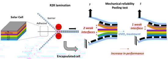
The commercial viability of roll-to-roll manufactured OPVs hinges on effective encapsulation techniques. Encapsulation is essential for protecting organic materials from environmental degradation. Juillard et al.
[77] investigated the impact of roll-to-roll flexible encapsulation on OPV devices, focusing on mitigating environmental degradation and enhancing device longevity. They conducted a comprehensive assessment of both the performance and mechanical reliability of encapsulated devices. Using a novel peeling technique, the authors analyzed the interfacial strengths within multilayered OPV devices on a flexible poly(ethylene terephthalate) substrate. This approach revealed significant weaknesses at two specific interfaces: between the active layer and the hole-transporting layer and between the transparent conducting electrode and the electron-transporting layer. To correct the weakness, the group explored various surface treatments, finding that optimized UV–ozone treatment significantly improved the adhesion of zinc oxide (ZnO) layers, as confirmed by IR spectroscopy and contact angle measurements (see
Figure 4). The study concluded that enhancing interfacial adhesion not only improves device performance but also increases resilience to the stresses of roll-to-roll encapsulation.
Figure 4. Process flow for enhancing the durability and performance of organic photovoltaic devices. The illustration shows a multilayered solar cell structure being encapsulated through roll-to-roll (R2R) lamination, identifying two weak interfaces that are prone to separation. A mechanical peeling test is used to assess the mechanical reliability. Subsequently, UV–ozone (UVO
3) treatment is applied to one of the interfaces, resulting in improved adhesion, a reduction to one weak interface, and an overall increase in the solar cell’s performance. Reprinted with permission from ref.
[77], copyright 2018, ACS Applied Materials and Interfaces.
Recent advancements have seen OPVs achieve significantly increased efficiencies, especially in indoor lighting conditions. Cui et al.
[75] reported on the potential of OPV cells for indoor applications. OPV technology, characterized by its capacity for large-area, lightweight, and flexible solar panel production via low-cost roll-to-roll methods, has seen rapid improvements in its power conversion efficiency (PCE). Specifically, the group optimized OPV cells for indoor lighting conditions, achieving a top PCE of 22% with 1 cm
2 cells under 1000 lux LED illumination. These cells also exhibited enhanced stability under continuous indoor light, underscoring the importance of developing wide-bandgap active materials that are tailored for indoor OPV applications, which could significantly elevate the photovoltaic performance.
4.2. Performance Metrics: Efficiency and Stability
Organic photovoltaic cells (OPVs) have seen significant advancements in terms of their power conversion efficiency (PCE) and stability, two critical performance metrics in solar technology. Recent developments in OPV technology have led to substantial improvements in the PCE. A notable example is the work by Wang et al.
[78], where the authors explored the potential of OPV cells for indoor applications, addressing the challenge of energetic disorder under low illuminance. They demonstrated that concentrated indoor light mitigates energetic disorder, enhancing the open-circuit voltage and fill factor, with PB2:FCC-Cl (2,2′-((2Z,2′Z)-((12,13-bis(2-ethylhexyl)-3,9-diundecyl-12,13-dihydro-[1,2,5]thiadiazolo [3,4e]thieno[2″,3″:4′,5′]thieno[2′,3′:4,5]pyrrolo[3,2-g]thieno[2′,3′:4,5]thieno[3,2-b] indole-2,10-diyl)bis(methanylylidene)) bis(5,6-dicloro-3-oxo-2,3-dihydro-1H-indene-2,1-diylidene)) dimalononitrile)-based cells achieving a remarkable 33.0% PCE at 20,000 lux. Additionally, the group reported superior stability of OPV cells under such conditions, noting over 30,000 h of intrinsic lifetime for the PBDB-TF:Y6 ([(2,6-(4,8-bis(5- (2-ethylhexyl-3-fuoro)thiophen-2-yl)-benzo[1,2-b:4,5-b′]dithiophene))-alt-(5,5-(1′,3′-di-2-thienyl-5′,7′-bis(2-ethylhexyl)benzo [1′,2′-c:4′,5′-c′]dithiophene-4,8-dione))]: 2,2′-((2Z,2′Z)-((12,13-bis(2-ethylhexyl)-3,9-diundecyl-12,13-dihydro-[1,2,5]thiadiazolo[3,4e]thieno[2″,3″:4′,5′]thieno[2′,3′:4,5]pyrrolo[3,2-g]thieno[2′,3′:4,5]thieno[3,2-b] indole-2,10-diyl)bis(methanylylidene)) bis(5,6-difluoro-3-oxo-2,3-dihydro-1H-indene-2,1-diylidene)) dimalononitrile) system. The integration with optical waveguide concentrators suggests a pathway for low-cost manufacturing, underscoring the necessity of developing concentrated OPV cells for future indoor applications. Additionally, Ma et al.
[79] presented a strategy for enhancing both the mechanical robustness and photovoltaic performance of all-polymer OPV cells, making them suitable for flexible wearable devices. The authors introduced a high-molecular-weight polymer donor, PBDB-TF,into a PBQx-TF:PY-IT(poly[4,8-bis(5-(2-ethylhexyl)thiophen-2-yl)benzo[1,2-b;4,5-b′]dithiophene-2,6-diyl-alt-(4-(2-ethylhexyl)-3-fluorothieno[3,4-b]thiophene-2-carboxylate-2-6-diyl)]) blend to improve the bulk hetero-junction morphology, resulting in more efficient charge transport and enhanced mechanical stress dissipation. This ternary blend film yields OPV cells with a maximum PCE of 18.2% and an impressive fill factor of 0.796, maintaining a PCE of 16.5% even under mechanical stress, offering a viable approach to fortify all-polymer OPV cells.
Despite these efficiency improvements, stability remains a major challenge for OPVs. The organic materials that are used in OPVs are often more susceptible to environmental degradation factors like oxygen and moisture. Wu and team
[80] critically reviewed the recent research progress on the stability of high-performance OSCs, discussing factors limiting a device’s lifetime such as metastable morphology, air, irradiation, heat, and mechanical stresses. Their review emphasizes the need for ongoing research in material design and device engineering to enhance the stability of OPVs
[80].
The efficiency of OPVs under standard solar conditions still lags behind that of conventional solar cells. However, their performance in indoor environments, as demonstrated by Wang et al.
[78], suggests a niche where OPVs could be particularly effective. The unique spectral characteristics of indoor lighting compared to outdoor sunlight play a significant role in this context. The high tunability in the optical absorption and insensitivity to series resistance and active layer thickness make OPVs promising for indoor applications
[78].
The bandgap of semiconducting polymers is a fundamental property that determines the range of solar spectrum that an organic solar cell (OSC) can effectively absorb
[72]. The ideal bandgap for OSCs is typically in the range of 1.1 to 1.7 eV, which allows for optimal absorption of the solar spectrum while maintaining a high open-circuit voltage (Voc). Designing polymers with a specific bandgap requires precise control over the molecular structure, including the backbone conjugation length, the nature of side chains, and the introduction of donor or acceptor units within the polymer chain
[73][77].
One challenge in specifying the bandgap is the trade-off between a wide absorption spectrum and the Voc. A narrower bandgap can increase the absorption of photons, particularly in the near-infrared region, but it can also lead to a reduction in the Voc, diminishing the overall power conversion efficiency (PCE)
[68][71][72]. Conversely, a wider bandgap can enhance the Voc but at the expense of reducing the absorption range, leading to a decreased photocurrent. Molecular engineering strategies, such as the development of donor–acceptor (D-A) copolymers, have been employed to address this issue. These copolymers combine electron-rich (donor) and electron-deficient (acceptor) units, allowing for tunable bandgaps and improved absorption properties while maintaining satisfactory Voc levels
[72].
Charge dynamics, encompassing charge generation, transport, and collection, are critical for the efficiency of OSCs. Upon absorption of sunlight, excitons (bound electron–hole pairs) are generated within the polymer matrix
[74][80]. These excitons must dissociate into free charges and be transported to the electrodes without significant recombination losses.
The efficiency of exciton dissociation into free charges is highly dependent on the molecular architecture of the semiconducting polymers. The introduction of D-A interfaces within the polymer or between the polymer and a fullerene acceptor has been shown to facilitate exciton dissociation through the creation of charge transfer states
[79]. However, designing polymers that promote efficient charge generation while minimizing energy losses remains challenging.
The mobility of charges (electrons and holes) within semiconducting polymers is another critical factor. A high charge mobility is essential to minimize recombination losses and ensure efficient charge collection at the electrodes
[71]. The molecular ordering, crystallinity, and purity of the polymer significantly influence the charge mobility. Polymers with a high degree of crystallinity and ordered packing tend to exhibit higher charge mobilities. However, achieving such a high degree of order in solution-processed films is challenging. Molecular design strategies, including the introduction of side chains that promote self-organization and the synthesis of polymers with high molecular weights, have been explored to improve charge transport properties
[71][73].
Efficient charge collection at the electrodes is crucial for maximizing the PCE of OSCs. The alignment of energy levels between the semiconducting polymer and the electrode materials plays a vital role in facilitating charge collection
[76][77]. Misalignment can lead to significant energy barriers for charge extraction, increasing recombination losses. Molecular design strategies to tailor the end groups of polymers for better alignment with electrode materials are critical for optimizing the charge collection efficiency.
4.3. Technological Challenges and Prospects for Scalability
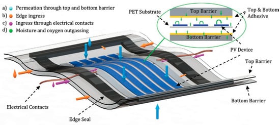
Scaling OPVs for widespread use involves overcoming several technological challenges, particularly concerning the inherent instability of organic materials and the complexities of large-scale production. The primary challenge in scaling OPVs is the inherent instability of organic materials. These materials can degrade under environmental stressors such as UV light, oxygen, and moisture. Sutherland et al.
[81] argue that the development of flexible barrier encapsulation is essential, which requires materials with exceptional moisture resistance, high transparency, and durability against mechanical stress. Their review discusses these challenges in detail and examines the latest advancements in flexible encapsulation materials, suggesting directions for future research.
Figure 5 shows four distinct routes through which moisture and oxygen can penetrate flexible encapsulated PSC and OPV devices.
Figure 5. The illustration shows four distinct routes through which moisture and oxygen can penetrate flexible encapsulated PSC and OPV devices, leading to expedited degradation and diminished operational life. The permeation through top and bottom barrier (a) is represented by the light blue arrows and droplet, (b) edge ingress is represented by the light brown droplet and arrows, (c) ingress through electrical contact is represented by the violet droplet and arrows, and (d) moisture and oxygen outgassing is represented by the green droplet and arrows Reprinted with permission from ref.
[81], copyright 2021, Advanced Energy Materials.
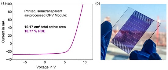
Transitioning from small-area lab cells to large-scale, industrially viable OPV modules presents significant challenges. Wachsmuth and colleagues
[82] explored the upscaling of OPVs from small-area lab cells to solution-processed modules that are compatible with industrial roll-to-roll (R2R) printing. This process involved meticulous material selection and optimization of each layer in the OPV stack, including the photoactive and charge-transporting layers, as well as the solution-processed top electrode. The authors also conducted long-term stability tests (thermal and light exposure) and successfully scaled up the device area by over 100 times. The result was a semitransparent OPV module with a 10.8% power conversion efficiency on a 10.2 cm
2 area, meeting industrial R2R printing requirements, thus paving the way for large-scale production (see
Figure 6).
Figure 6. The image shows (
a) the J-V curve and (
b) a photograph of a semitransparent module that has been fully processed in solution and in air. This module, positioned on a glass/ITO substrate, consists of eight cells connected in series and covers a total active area of 10.17 cm
2, including a back-reflector. Reprinted with permission from ref.
[82], copyright 2023, Solar RRL.
The future of OPVs in large-scale applications hinges on addressing these challenges. Continued advancements in material stability, encapsulation techniques, and upscaling processes are crucial for the long-term viability and commercial success of OPVs. As these technological hurdles are overcome, OPVs hold the promise of becoming a key player in the renewable energy sector, offering a sustainable and cost-effective alternative to traditional solar technologies.
 +1 credit