Your browser does not fully support modern features. Please upgrade for a smoother experience.
Submitted Successfully!
 +1 credit
Thank you for your contribution! You can also upload a video entry or images related to this topic.
For video creation, please contact our Academic Video Service.
| Version | Summary | Created by | Modification | Content Size | Created at | Operation |
|---|---|---|---|---|---|---|
| 1 | Laurentiu Fara | -- | 2061 | 2024-03-03 20:13:33 | | | |
| 2 | Fanny Huang | Meta information modification | 2061 | 2024-03-05 08:32:53 | | |
Video Upload Options
We provide professional Academic Video Service to translate complex research into visually appealing presentations. Would you like to try it?
Cite
If you have any further questions, please contact Encyclopedia Editorial Office.
Fara, L.; Chilibon, I.; Vasiliu, I.C.; Craciunescu, D.; Diaconu, A.; Fara, S. Experimental Approach to Silicon Heterojunction Tandem Solar Cells. Encyclopedia. Available online: https://encyclopedia.pub/entry/55789 (accessed on 24 June 2026).
Fara L, Chilibon I, Vasiliu IC, Craciunescu D, Diaconu A, Fara S. Experimental Approach to Silicon Heterojunction Tandem Solar Cells. Encyclopedia. Available at: https://encyclopedia.pub/entry/55789. Accessed June 24, 2026.
Fara, Laurentiu, Irinela Chilibon, Ileana Cristina Vasiliu, Dan Craciunescu, Alexandru Diaconu, Silvian Fara. "Experimental Approach to Silicon Heterojunction Tandem Solar Cells" Encyclopedia, https://encyclopedia.pub/entry/55789 (accessed June 24, 2026).
Fara, L., Chilibon, I., Vasiliu, I.C., Craciunescu, D., Diaconu, A., & Fara, S. (2024, March 03). Experimental Approach to Silicon Heterojunction Tandem Solar Cells. In Encyclopedia. https://encyclopedia.pub/entry/55789
Fara, Laurentiu, et al. "Experimental Approach to Silicon Heterojunction Tandem Solar Cells." Encyclopedia. Web. 03 March, 2024.
Copy Citation
A solar cell, or a photovoltaic (PV) cell, is an electrical device that converts light energy directly into electricity by the photovoltaic effect. There are different types of solar cells. Tandem solar cells could have a very good conversion efficiency in comparison with other types of solar cells. Tandem solar cells are considered the industry’s next step in photovoltaics due to their excellent conversion efficiency. A very good example is the perovskite absorber material that has been developed for efficient tandem solar cells.
Cu2O/c-Si tandem heterojunction SC
perovskite
silicon heterojunction tandem solar cells (SHTSCs)
1. Introduction
A solar cell, or a photovoltaic (PV) cell, is an electrical device that converts light energy directly into electricity by the photovoltaic effect. The operation of a photovoltaic (PV) cell requires three essential features: (a) the absorption of light, generating electron–hole pairs; (b) the separation of charge carriers of opposite types; and (c) the separate extraction of those carriers to an external circuit.
There are different types of solar cells: (1) amorphous silicon (A-Si) solar cells; (2) biohybrid solar cells (which are based on a combination of organic and inorganic matter); (3) silicon buried-contact solar cells; (4) cadmium telluride solar cells; (5) concentrated PV (CPV) cells; (6) copper indium gallium selenide (CIGS) solar cells; (7) dye-sensitized solar cells (DSSCs); (8) gallium arsenide solar cells (GaAs SCs); (9) hybrid polymer solar cells (HPSCs); (10) luminescent solar concentrator cells (LSCCs); (11) monocrystalline silicon solar cells (Mono-Si SCs); (12) polycrystalline silicon solar cells (Poly-Si SCs); (13) multijunction solar cells (MJSCs); (14) quantum dot solar cells (QDSCs); (15) tandem solar cells (TSCs).
Tandem solar cells could have a very good conversion efficiency in comparison with other types of solar cells. Tandem solar cells use two different materials that absorb solar radiation; this means that a tandem solar cell can absorb more of the solar spectrum—and so produce more electricity—than if one material is used (such as silicon solar cells).
Tandem solar cells are considered the industry’s next step in photovoltaics due to their excellent conversion efficiency. A very good example is the perovskite absorber material that has been developed for efficient tandem solar cells. The European Solar Test Installation has verified a 32.5% efficiency for perovskite/silicon tandem solar cells.
Solutions related to tandem solar cells based on silicon are studied, using three advanced architectures with different material structures, namely, metal oxide, thin film, and perovskite [1][2].
1.1. Metal Oxide Tandem Heterojunction Solar Cells
Currently, more than 90% of the photovoltaic (PV) market is dominated by crystalline Si solar cells [3]. Silicon-based tandem heterojunction solar cells having a metal-oxide subcell represent an attractive approach in the development of the next generation of SCs.
Cutting the cost of PV-producing technology would be possible if low-cost metal oxides were used in fabrication of Si-based tandem solar cells to be developed further.
Cuprous oxide (Cu2O), as a p-type semiconductor with high optical absorption and a direct bandgap of about 2.1 eV, is suggested to be a good match for PV applications. A p-n heterojunction could be designed and fabricated using an n-type semiconductor such as ZnO. As both TiO2 and ZnO are low-cost oxides, the premises to develop a low-cost heterojunction solar cell are met. Since only 8% conversion efficiency has been achieved experimentally to date [4][5], further investigation of Cu2O-based solar cells could create the premises to fully achieve the potential of PV technology, as it is known that the maximum theoretical efficiency of such SCs is 19% [6][7].
Three different versions of flexible ZnO/Cu2O solar cells have been developed, respectively: (1) thin film; (2) nanowire; and (3) nanotube [8]. ZnO nanowires and nanotubes are implied to have higher efficiency than thin films, at about 0.12%. ZnO thin films have relatively low efficiency of 0.02%.
The key limitations of the power conversion efficiency (PCE) of a metal oxide SHTSC are given by three factors: material and charge collector quality, material absorption coefficient, and interface quality. Thus, special efforts must be made to understand SHTSC behaviour and the most important parameters for achieving optimum performance.
1.2. III–V Tandem Solar Cells
A III–V tandem SC with 6 junctions is characterized by an efficiency of 47.1% under concentrated solar irradiance [9]. Tandem SCs using Si as a bottom cell, with a high efficiency, are classified conceptually as III–V/Si. For the cases of 2-junction GaAs/Si SC, and 3-junction GaInP/GaAs/Si SC the maximum efficiency values obtained are 32.8% and 35.9%, respectively.
New investigations have shown an increased efficiency for 2-junction and 3-junction SCs designed by direct growth technology. At the same time, smart stacking technology confers a significant efficiency advantage. It has been noted that the cost of a Si-based III–V tandem SC is lower than that of a III–V tandem SC. The usual degradation conditions are defined by heat, moisture, oxygen, and UV radiation, leading to long-term stability. Thus, Si-based III–V tandem SCs are very stable and reliable.
Plasmonic Solar Cells
An improved approach of increased efficiency for SHTSCs based on metal oxides can be applied for III–V tandem SCs by incorporating plasmonic nanocomponents [10]. Due to their ability to scatter light back into the PV structure and their low absorption, plasmonic nanoparticles are studied as a method for increasing solar cells’ efficiency [10][11][12].
The plasmons excited by optical radiation induce an electric current from hot electrons in materials made from gold particles and light-sensitive molecules of porphin. The wavelength to which the plasmon responds is a function of the size and distance between particles. The material is made by ferroelectric nanolithography. Compared to conventional photoexcitation, the material produces three to ten times the current [13][14]. The same idea applies to the discussion of perovskite tandem SCs [15].
Metallization is performed on doped regions at either low or high temperatures. Low-temperature metal contacts can be made in Ni/Si, ITO/a-Si, or ITO/Si configurations. High-temperature metallization is based on screen printing and simultaneous annealing of Al (positive) and Ag (negative) paste contacts in a conveyor-belt furnace as it transits across multiple temperature zones.
1.3. Perovskite Tandem Solar Cells
The highest verified efficiency obtained for perovskite tandem SCs to date is 29.15% [11]. Rapid improvements have been made for tandem perovskite/Si-based SCs, with the advantage of much lower cost. For perovskite/Si solar cells, the laboratory performance record achieved is 32.5%. Most of the existing high-efficiency perovskite tandem SCs are technologically acceptable for low-cost SCs; specifically, the estimated cost of perovskite SCs is one-third of the cost of Si SCs. In contrast, the long-term stability of perovskite/Si-based SCs is low because moisture causes deterioration of its performance. Therefore, special efforts are needed to prevent this degradation. Perovskite SCs have shorter lifetimes, ranging from a few days to months and up to a year at most. It is imperative to study, develop and test a long-life perovskite tandem SC. For perovskite SCs, the requirements are increases in efficiency and long-term stability, along with reductions in manufacturing costs. However, there have been promising approaches for simultaneously achieving higher efficiency and stability. As perspective, there is much more open potential for the coming years.
2. The Fundamental Idea of SHTSCs
The tandem solar cell is composed of (i) a top subcell formed from an Al-ZnO/Cu2O heterojunction and (ii) a bottom subcell based on c-Si. The visible-light transparency and the electrical conductivity of the ZnO layer are improved as a result of Al doping. That is why an Al-doped ZnO layer would represent a promising transparent conducting electrode for nano-optoelectronic solar devices [16].
The proposed approach aims at increasing of the power efficiency beyond the conventional limit of the Si solar cell. Through the top subcell, the low-energy photons are transmitted, while through the bottom subcell, the high-energy photons are absorbed. Thus, a 4-terminal configuration for the tandem solar device was determined because the current density of the top subcell is half that of the bottom subcell.
A layer of cuprous oxide (Cu2O) can act as a photoabsorber [6][7][8][9][17]. Cu2O is preferred due to the following main merits: (1) it is present in great quantities on earth; (2) it has reduced toxicity, and (3) it has low costs of synthesis. The main characteristics that qualify it for photovoltaic applications are the following: (1) Cu2O is a p-type semiconductor; (2) its bandgap is Ego = 2.1 eV; (3) it has a high absorption coefficient of 105 cm−1; (4) its absorption edge is sharp; (5) it has a high carrier mobility (100 cm2 V−1 s−1); (6) the electron affinity is low (3.2 eV); (7) it has band offsets with an n-type heterojunction partner; (8) the heat of formation is low (−171 kJ/mol); and (9) the interface is prone to oxidation and formation of an interface defect layer (IDL). Theoretically, the conversion efficiency of the copper oxide layer is 19%, but experimentally, a maximum conversion efficiency of only 8% has been obtained.
3. SHTSC Experimental Approach: Deposition, Characterization, and Physical Parameters of Cu2O Films
3.1. Cu2O Films Deposition by a Sputtering System
A magnetron sputtering method was used to deposit Cu2O films on a quartz substrate [18][19][20][21][22]. The Cu target was placed in O2/Ar, and the substrate temperature was kept at 400 °C. Cu2O films with a thickness of around 500 nm were deposited at a rate of ~25 nm/min, then further annealed at 900 °C and p~0.1 Torr for 3 min.
An Al-doped ZnO layer was deposited by co-sputtering of a 99.99% ZnO target and a 99.999% Al target in an Ar atmosphere using a 400 °C substrate temperature.
This innovative solution would contribute to the achievement of an improved solar cell by using low-cost materials and non-toxic metal oxides, which remove the disadvantages of conventional solar cells.
3.2. Morphological Characterization of Cu2O Films
A scanning electron microscope (SEM) equipped with an electron emission gun was used to investigate the morphology of the Cu2O film samples [22][23] with a resolution of 1.2 nm.
The average grain size increased after the annealing, as noticed from the SEM images of 500 nm thick Cu2O coatings as grown (Figure 1) and annealed at 900 °C (Figure 2).
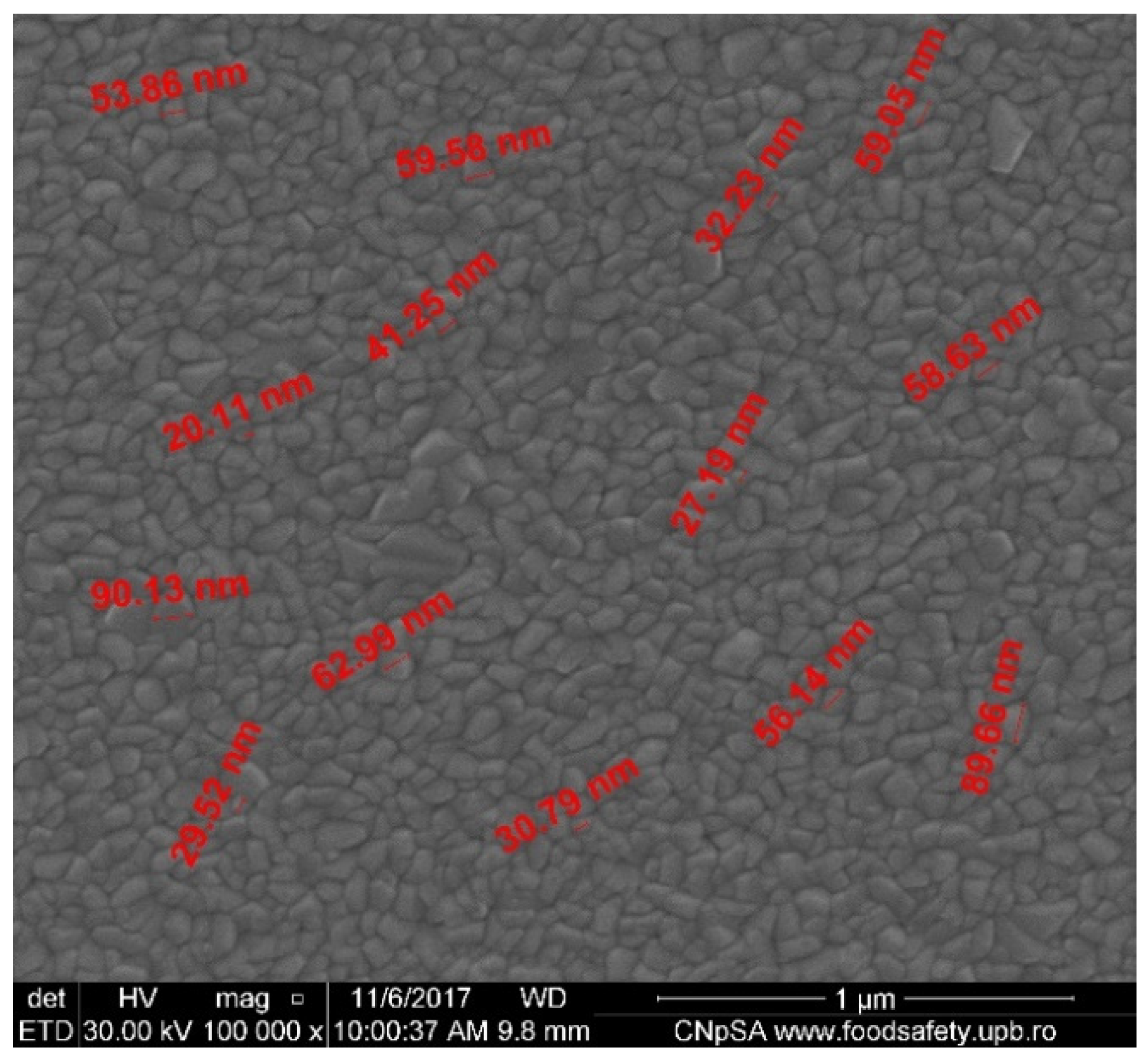
Figure 1. SEM image of as-grown Cu2O film, 500 nm thickness.
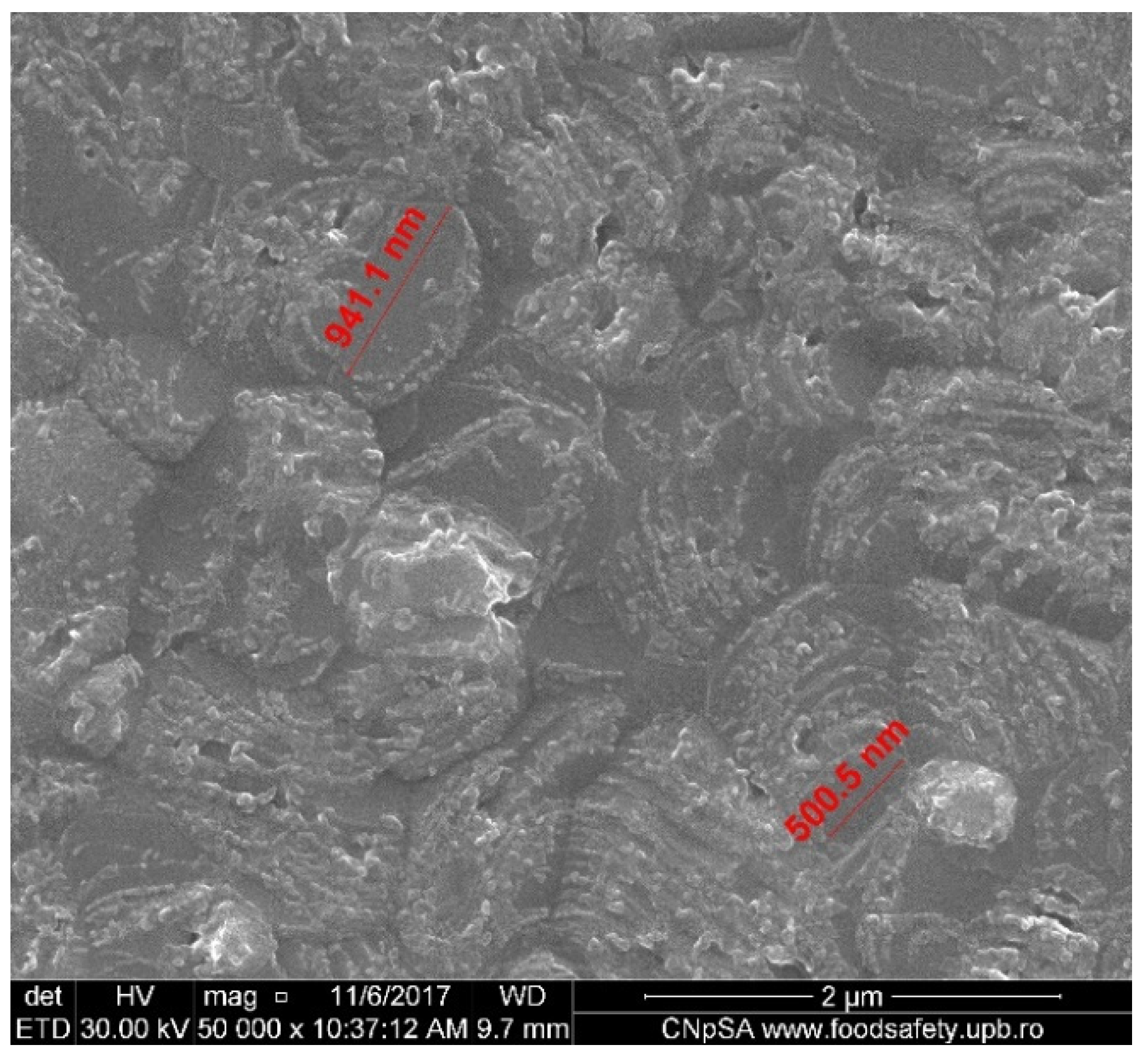
Figure 2. SEM image of Cu2O film annealed at 900 °C, 500 nm thickness.
At the same time the samples were analysed using an atomic force microscope (AFM), with a Si-doped probe. It was noted that the surface roughness RRMS for the as-grown Cu2O coatings deposited on quartz increases after annealing at 900 °C for 3 min in vacuum, and the largest RRMS reaches about 21 nm the largest RRMS [23].
3.3. Optical Characterization of Cu2O Films
The X-ray fluorescence measurements were carried out using an XRF material analyser [24]. An ellipsometer in the wavelength range of 190 to 2100 nm allowed the determination of the film thickness and complex refractive index [25][26]. Delta psi was the model used to fit the measured ellipsometry parameters.
It was noticed that the optical transmittance properties of the Cu2O films were improved in the Vis and near-IR wavelength range after annealing, which is likely to be due to the larger grain size and a corresponding reduction in grain-boundary scattering, possibly together with less strained film [22][27].
It was suggested that the effect of broadening of the optical band gap after annealing might be due to partial elimination of defects and possibly to less contaminated Cu2O films. In this way, the optical band gap increases from Eg = 2.06 eV for as-grown Cu2O film to Eg = 2.19 eV after annealing at 900 °C.
The energy-dispersive X-ray spectroscopy (EDX) spectrum for Cu2O film of 500 nm thickness (Figure 3) revealed the composition of the film, namely, the net Cu/O gravimetric ratio of the sample. It is suggested that the gravimetric ratio of the Cu2O film deposited by magnetron sputtering is Cu/O = 4:1, which means that there are mostly Cu2O compounds of high purity.
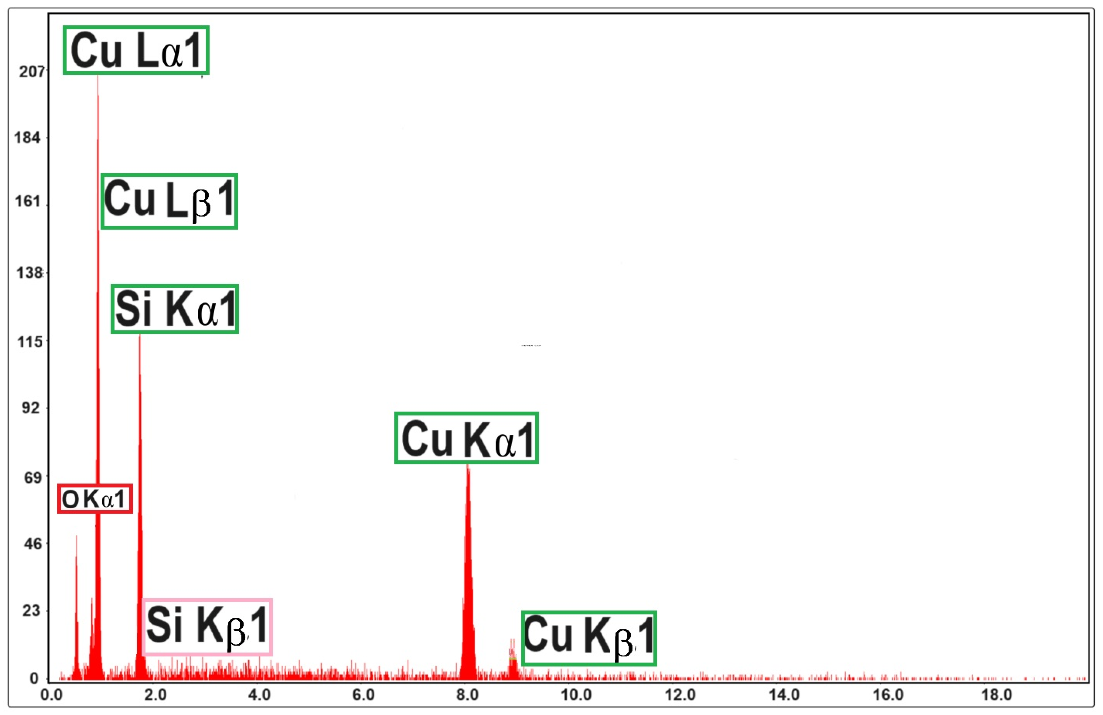
Figure 3. EDX spectrum for Cu2O film of 500 nm thickness, deposited by magnetron sputtering on quartz substrate.
3.4. Physical Parameters of Cu2O Films
The measurements of the Hall effect at room temperature were carried out using the van der Pauw configuration. The room-temperature Hall effect measurements allowed the evaluation of hole mobility, film resistivity, and hole concentration for the 500 nm thick as-grown and annealed Cu2O films on quartz. The majority carrier (hole) mobility of the Cu2O coatings increased from 10 to 50 cm2 V−1 s−1 after annealing, and the resistivity decreased from 560 to 200 Ω·cm [28][29]. These values are comparable to those reported previously for sputter-deposited polycrystalline Cu2O films on quartz [21][30], which suggests that the annealed Cu2O thin films are well suited for photovoltaic applications. The increase in the carrier mobility after annealing could be attributed to the increase in grain size and reduced grain-boundary scattering.
References
- Saif, O.M.; Zekry, A.H.; Abouelatta, M.; Shaker, A. A Comprehensive Review of Tandem Solar Cells Integrated on Silicon Substrate: III/V vs. Perovskite. Silicon 2023, 15, 6329–6347.
- Wilson, G.M.; Al-Jassim, M.; Metzger, W.K.; Glunz, S.W.; Verlinden, P.; Xiong, G.; Mansfield, L.M.; Stanbery, B.J.; Zhu, K.; Yan, Y.; et al. The 2020 photovoltaic technologies roadmap. J. Phys. D Appl. Phys. 2020, 53, 493001.
- Fara, L.; Chilibon, I.; Nordseth, Ø.; Craciunescu, D.; Savastru, D.; Vasiliu, C.; Baschir, L.; Fara, S.; Kumar, R.; Monakhov, E.; et al. Complex Investigation of High Efficiency and Reliable Heterojunction Solar Cell based on an Improved Cu2O Absorber Layer. Energies 2020, 13, 4667.
- Nordseth, Ø.; Kumar, R.; Bergum, K.; Fara, L.; Foss, S.E.; Haug, H.; Dragan, F.; Craciunescu, D.; Sterian, P.; Chilibon, I.; et al. Optical Analysis of a ZnO/Cu2O Subcell in a Silicon-Based Tandem Heterojunction Solar Cell. Green Sustain. Chem. (GSC) 2017, 7, 57–69.
- Takiguchi, Y.; Miyajima, S. Device simulation of cuprous oxide heterojunction solar cells. Jpn. J. Appl. Phys. 2015, 54, 112303.
- Wong, T.K.S.; Zhuk, S.; Masudy-Panah, S.; Dalapati, G.K. Current status and future prospects of copper oxide heterojunction solar cells. Materials 2016, 9, 271.
- Fara, L.; Chilibon, I.; Craciunescu, D.; Diaconu, A.; Fara, S. Review, Heterojunction Tandem Solar Cells on Si-Based Metal Oxides. Energies 2023, 16, 3033.
- Wei, H.; Gong, H.; Wang, Y.; Hu, X.; Chen, L.; Xu, H.; Liu, P.; Cao, B. Three kinds of Cu2O/ZnO heterostructure solar cells fabricated with electrochemical deposition and their structure-related photovoltaic properties. CrystEngComm 2011, 13, 6065–6070.
- Heinrich, M.; Kuhn, T.E.; Dimroth, F.; Würfel, U.; Goldschmidt, J.C.; Powalla, M.; Glunz, S.W.; Neuhaus, D.H. A comparison of different solar cell technologies for integrated photovoltaics. In Proceedings of the 37th European Photovoltaic Solar Energy Conference and Exhibition, EU PVSEC, Online, 7–11 September 2020; pp. 1984–1994.
- Zaidi, S.H. Metallization in Solar Cell. In Crystalline Silicon Solar Cells; Springer: Cham, Switzerland, 2021; pp. 125–200.
- Ashouri, A.A.; Köhnen, E.; Li, B.; Magomedov, A.; Hempel, H.; Caprioglio, P.; Márquez, J.A.; Morales Vilches, A.B.; Kasparavicius, E.; Smith, J.A.; et al. Monolithic perovskite/silicon tandem solar cell with >29% efficiency by enhanced hole extraction. Science 2020, 370, 1300–1309.
- Yue, Z.; Cai, B.; Wang, L.; Wang, X.; Gu, M. Intrinsically core-shell plasmonic dielectric nanostructures with ultrahigh refractive index. Sci. Adv. 2016, 2, e1501536.
- Yu, P.; Yao, Y.; Wu, J.; Niu, X.; Rogach, A.L.; Wang, Z. Effects of Plasmonic Metal Core -Dielectric Shell Nanoparticles on the Broadband Light Absorption Enhancement in Thin Film Solar Cells. Sci. Rep. 2017, 7, 7696.
- Ferry, V.E.; Munday, J.N.; Atwater, H.A. Design Considerations for Plasmonic Photovoltaics. Adv. Mater. 2010, 22, 4794–4808.
- Laska, M.; Krzemińska, Z.; Kluczyk-Korch, K.; Schaadt, D.; Popko, E.; Jacak, W.A.; Jacak, J.E. Methods for increasing efficiency should be indicated, including nano-metallization. Nano Energy 2020, 75, 104751.
- Wu, M.; Sun, D.; Tan, C.; Tian, X.; Huang, Y. Al-Doped ZnO Monolayer as a Promising Transparent Electrode Material: A First-Principles Study. Materials 2017, 10, 359.
- Svensson, B.G.; Pearton, S.J.; Jagadish, C. Oxide Semiconductors, Semiconductors and Semimetals; Elsevier & Academic Press: Amsterdam, The Netherlands, 2013.
- Minami, T.; Nishi, Y.; Miyata, T. Efficiency enhancement using a Zn1−x Gex -O thin film as an n-type window layer in Cu2O-based heterojunction solar cells. Appl. Phys. Express 2016, 9, 052301.
- Minami, T.; Miyata, T.; Nishi, Y. Cu2O-based heterojunction solar cells with an Al-doped ZnO/oxide semiconductor/thermally oxidized Cu2O sheet structure. Sol. Energy 2014, 105, 206–217.
- Gan, J.; Venkatachalapathy, V.; Svensson, B.G.; Monakhov, E.V. Influence of Target Power on Properties of CuxO Thin Films Prepared by Reactive Radio Frequency Magnetron Sputtering. Thin Solid Film. 2015, 594, 250–255.
- Ishizuka, S.; Maruyama, T.; Akimoto, K. Thin-film deposition of Cu2O by reactive radiofrequency magnetron sputtering. Jpn. J. Appl. Phys. 2000, 39, L786–L788.
- Nordseth, Ø.; Chilibon, I.; Kumar, R.; Bergum, K.; Vasiliu, C.; Iordanescu, R.; Baschir, L.; Savastru, D.; Kiss, A.; Parau, A.; et al. Characterization of Cuprous Oxide Thin Films Prepared by Reactive Direct Current Magnetron Sputtering. Sens. Transducers 2018, 220, 53–60.
- Read, D.T.; Cheng, Y.W.; Geiss, R. Morphology, microstructure, and mechanical properties of a copper electrodeposit. Microelectron. Eng. 2004, 75, 63–70.
- Chilibon, I.; Fara, L.; Nordseth, Ø.; Kumar, R.; Svensscen, B.G.; Dumitru, C.; Dragan, F.; Muscurel, V.; Vasiliu, C.; Stefan, R. Characterization of Cuprous Oxide Thin Films used in solar cells by fluorescence and FTIR spectroscopy. AOSR Ann. 2018, 11, 61–69.
- Chilibon, I.; Fara, L.; Nordseth, Ø.; Kumar, R.; Svensson, B.G.; Dumitru, C.; Dragan, F.; Muscurel, V.; Vasiliu, C.; Parau, A. Structural and electrical analysis of Cu2O layers for solar cell application. AOSR Ann. 2018, 11, 53–60.
- Nordseth, Ø.; Foss, S.E.; Svensson, B.G.; Kumar, R.; Chilibon, I.; Vasiliu, C.; Iordanescu, R.; Baschir, L.; Savastru, D.; Kiss, A.; et al. Cu2O photosensitive thin films for solar cell application. In Proceedings of the Sensor Devices, Rome, Italy, 10–14 September 2017; pp. 47–52.
- Elmahdy, M.M.; El-Shaer, A. Structural, optical and dielectric investigations of electrodeposited p-type Cu2O. J. Mater. Sci. Mater. Electron. 2019, 30, 19894–19905.
- Nordseth, Ø.; Kumar, R.; Bergum, K.; Fara, L.; Chilibon, I.; Foss, S.E.; Monakhov, E.; Svensson, B.G. Silicon-based tandem solar cells Boosting the performance using non-toxic metal oxides. GIT Lab. J. 2017, 7–8, 25–27.
- Bergum, K.; Riise, H.N.; Gorantla, S.; Lindberg, P.F.; Jensen, I.J.T.; Gunnæs, A.E.; Galeckas, A.; Diplas, S.; Svensson, B.G.; Monakhov, E. Improving carrier transport in Cu2O thin films by rapid thermal annealing. J. Phys. Condens. Matter. 2018, 30, 075702.
- Zhu, H.; Zhang, J.; Li, C.; Pan, F.; Wang, T.; Huang, B. Cu2O thin films deposited by reactive direct current magnetron sputtering. Thin Solid Films 2009, 517, 5700–5704.
More
Information
Subjects:
Physics, Applied
Contributors
MDPI registered users' name will be linked to their SciProfiles pages. To register with us, please refer to https://encyclopedia.pub/register
:
View Times:
756
Revisions:
2 times
(View History)
Update Date:
05 Mar 2024
Table of Contents


Notice
You are not a member of the advisory board for this topic. If you want to update advisory board member profile, please contact office@encyclopedia.pub.
OK
Confirm
Only members of the Encyclopedia advisory board for this topic are allowed to note entries. Would you like to become an advisory board member of the Encyclopedia?
Yes
No
${ textCharacter }/${ maxCharacter }
Submit
Cancel
Back
Comments
${ item }
|
${ item.createdUser.fullName }
${ item.createdAt }
${ item.vote }
${ item.reply }
Delete
${ reply.createdUser.fullName }
${ reply.createdAt }
${ reply.vote }
Delete
There is no reply to this comment~
${ item.replyTextCharacter }/${ item.replyMaxCharacter }
Submit
Cancel
More
No more~
There is no comment~
${ textCharacter }/${ maxCharacter }
Submit
Cancel
${ selectedItem.replyTextCharacter }/${ selectedItem.replyMaxCharacter }
Submit
Cancel
Confirm
Are you sure to Delete?
Yes
No