Your browser does not fully support modern features. Please upgrade for a smoother experience.
Submitted Successfully!
 +1 credit
Thank you for your contribution! You can also upload a video entry or images related to this topic.
For video creation, please contact our Academic Video Service.
| Version | Summary | Created by | Modification | Content Size | Created at | Operation |
|---|---|---|---|---|---|---|
| 1 | Peng Gao | -- | 3009 | 2024-02-27 10:05:54 | | | |
| 2 | Lindsay Dong | Meta information modification | 3009 | 2024-02-28 04:19:22 | | |
Video Upload Options
We provide professional Academic Video Service to translate complex research into visually appealing presentations. Would you like to try it?
Cite
If you have any further questions, please contact Encyclopedia Editorial Office.
Wu, S.; Li, C.; Lien, S.Y.; Gao, P. Annealing Methods for Perovskite Solar Cells. Encyclopedia. Available online: https://encyclopedia.pub/entry/55514 (accessed on 24 June 2026).
Wu S, Li C, Lien SY, Gao P. Annealing Methods for Perovskite Solar Cells. Encyclopedia. Available at: https://encyclopedia.pub/entry/55514. Accessed June 24, 2026.
Wu, Shengcong, Chi Li, Shui Yang Lien, Peng Gao. "Annealing Methods for Perovskite Solar Cells" Encyclopedia, https://encyclopedia.pub/entry/55514 (accessed June 24, 2026).
Wu, S., Li, C., Lien, S.Y., & Gao, P. (2024, February 27). Annealing Methods for Perovskite Solar Cells. In Encyclopedia. https://encyclopedia.pub/entry/55514
Wu, Shengcong, et al. "Annealing Methods for Perovskite Solar Cells." Encyclopedia. Web. 27 February, 2024.
Copy Citation
Perovskite solar cells (PSCs) have garnered significant attention in the photovoltaic field owing to their exceptional photoelectric properties, including high light absorption, extensive carrier diffusion distance, and an adjustable band gap. Temperature is a crucial factor influencing both the preparation and performance of perovskite solar cells. The annealing temperature exerts a pronounced impact on the device structure, while the operational temperature influences carrier transport, perovskite band gap, and interface properties.
temperature
annealing
perovskite
hole transport layer
1. Introduction
Solar energy represents a sustainable and environmentally friendly power source, with solar photovoltaic devices serving as instrumental tools for converting solar energy into electricity. Over the past decade, perovskite solar cells (PSCs) have undergone rapid development, capturing widespread attention and engendering substantial research interest within the global scientific community [1][2]. The exceptional properties of perovskite, including a broad light absorption range, extensive carrier diffusion length, and low exciton binding energy, underscore its potential for widespread application [3]. As the conversion rate of PSCs continues to advance, there is an optimistic anticipation of their large-scale commercial production. Some experts even project the feasibility of achieving mass production of perovskite photovoltaics by the year 2025 [4].
PSCs can be generally divided into two categories: flexible perovskite solar cells (FPSCs) and rigid perovskite solar cells. FPSCs usually use a polymer substrate (e.g., polyethylene 2, 6-naphthalene diformate (PEN), or polyethylene terephthalate (PET)), and these polymer substrates have poor stability at high temperatures. Therefore, FPSCs usually need to be prepared under low-temperature conditions, and the preparation temperature of TiOx and NiOx is relatively high, so FPSCs are not suitable for the high-temperature preparation step of such substances. In PSCs, the perovskite layer is sandwiched between the electron transport layer (ETL) and the hole transport layer (HTL). PSCs mainly have two different structural types: normal (n-i-p structure, including mesoscopic structure) and inverted structure (p-i-n structure). Due to the high preparation temperature of mesoporous structures, they are generally not suitable for inverted structures. n-i-p-structured devices are constructed of transparent electrode/electron transport layer/mesoporous layer/perovskite layer/hole transport layer/counter electrode. The mesoporous layer is a scaffold, and perovskite material is filled in the mesoporous layer, which is responsible for assisting the separation of photogenerated carriers and avoiding direct contact between the HTL and the ETL. Sunlight passes through the transparent electrode and the ETL before it is absorbed by the perovskite film and finally converted into free carriers. The holes are transferred to the outer circuit along the HTL and the opposite electrode. Electrons are transferred to the external circuit along the electron transport layer and transparent electrode. In the planar structure, the perovskite film is deposited on the carrier transport layer, and direct contact is formed between the two functional layers, which simplifies the device preparation process.
In contrast to the normal planar structure, the inverted planar structure first deposits HTL on the substrate. p-i-n-structured devices are constructed of transparent electrode/HTL/perovskite layer/ETL/metal electrode. The perovskite film absorbs sunlight after passing through transparent electrodes and HTL and is finally converted into free carriers. The electrons and holes are transferred from the metal electrode and the transparent electrode to the external circuit, respectively.
Since normal PSCs have a different structure from the inverted PSCs, the ETL and HTL need to have different characteristics. The structure of PSCs as shown in Figure 1. For normal PSCs, since HTL is located on top of the perovskite layer, it needs to be highly hydrophobic. It can act as an effective protective layer for perovskite against moisture exposure. However, in inverted PSCs, HTL is deposited first. Then, perovskite is deposited on top of HTL, so HTL for inverted PSCs requires suitable surface wettability as a substrate for subsequent deposition and crystallization of perovskite [5]. In addition, since sunlight needs to pass through HTL first, the light transmissivity of HTL in inverted PSCs will also affect the light absorption efficiency of the perovskite layer [6]. In addition, the HTL thickness of inverted devices is always thin, so the requirement for hole mobility is not as high as that of conventional devices [7].
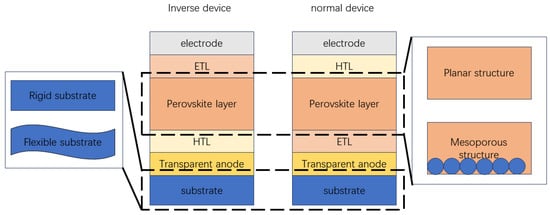
Figure 1. The structure of PSCs.
The fabrication of PSCs almost invariably involves high-temperature annealing [8][9]. This crucial step not only enhances film quality by increasing grain size, eliminating inter-grain cracks, and achieving a compact, smooth film but also boosts light absorption, reduces internal defects, and extends carrier lifetime. Consequently, annealing temperature emerges as a pivotal factor significantly influencing both the fabrication process and the performance of PSCs [10][11]. In summary, temperature exerts influence across various aspects: (i) concerning the electron transport layer (ETL), it accelerates crystallization, eliminates defects, and enhances substrate adhesion; (ii) alongside the conventional hotplate annealing method, new approaches such as rapid thermal annealing (RTA), intense pulsed light (IPL), liquid medium annealing (LMA), and post-annealing microwave treatment (MPAT) have emerged; (iii) the actual operational environment, marked by fluctuating temperatures, significantly impacts the performance of photovoltaic devices, altering the band gap of the light-absorbing layer and influencing carrier transport at the interface.
2. Temperature Control in Processing and Preparation
2.1. Electron Transport Layer
2.1.1. TiO2
The TiO2 is generally used as the ETLs of PSCs, which guarantee electron injection from the perovskite layer to the ETL by direct contact, and its VBM is at a shallow position, which gives TiO2 excellent hole-blocking properties. In addition, it is easy to control the morphology well, and its refractive index is low. There are many methods to prepare TiO2 layers for PSCs, such as spin-coating (hydrolysis [12], nanoparticles [13]), spray pyrolysis [14], chemical bath deposition (CBD) [15], atomic layer deposition (ALD) [16], and electrochemical deposition [17].
2.1.2. ZnO
ZnO is a widely used ETL material that has attracted much attention. ZnO is a semiconductor material with a direct band gap (3.11–3.36 eV) with an exciton binding energy of 60 meV. Compared with TiO2, ZnO has higher electron mobility and lower growth temperature. In addition, ZnO-based PSCs are superior in fulfilling application demands owing to their relatively lower cost, more straightforward deposition process, milder sintering temperatures, and higher electron mobility (~200 cm2/Vs). It is stable, low in price, provides environmental protection, and has other chemical characteristics. Since ZnO is almost soluble in water, it is often used for solution-based processing at lower temperatures. Its appearance is a white to yellowish-white crystalline substance. There are three forms of ZnO: cubic zinc blende, hexagonal wurtzite, and cubic rock salt [18].
2.1.3. SnO2
SnO2 is an efficient ETL material with excellent bulk electron mobility, deep conduction bands, and good energy levels. SnO2 exhibits excellent chemical stability, U.V. resistance, good antireflection, and less photocatalytic activity. In addition, SnO2 has a small refractive index and wide optical band gap (3.6–4.0 eV), resulting in high transmittance across the entire visible spectrum [19]. SnO2 compact ETLs were prepared through a simple sol–gel technique and used for the first time as an ETL in PSCs by Dong et al. in 2015 [20], the sintering process in a furnace at 450 °C. The best PCE is 9.83%.
2.1.4. PCBM
Phenyl-C61-methyl butyrate (PCBM) is one of the most used ETL materials in inverted PSCs. PCBM is considered to be a good electron acceptor (Lewis acid) and is inactivative to the perovskite layer [21]. PCBM was first used to invert PSCs in 2013 [22]. Lam et al. used PCBM as an ETL to understand the high performance of MAPbI3 solar cells [23]. It was found that PCBM plays a decisive role in inhibiting halide ion migration in the perovskite layer through halide-π non-covalent interaction. This interaction increases electron transport in the ETL [24].
2.2. Hole Transport Layer
The role of the hole transport layer is to transport holes to the TCO. Therefore, hole transport layer (HTL) materials should have high hole mobility and be able to block electrons. The hole transport layer should also have a certain degree of stability, not readily react with adjacent layers, and not quickly decompose under wet and high-temperature conditions. To save the cost of preparing PSCs entirely, studying HTL materials that can be prepared at lower temperatures is necessary. Materials commonly used as hole transport layers include spiro-OMeTAD, PTAA [25], PEDOT:PSS, and NiOx.
2.2.1. NiOx
NiO is a direct bandgap inorganic material with a band gap range of 3.6~4.0 eV and a work function of 5.4 eV [26]. It has the characteristics of high light transmission and electron blocking and should have good ohmic contact with the electrode. NiO also has good thermal stability, reasonable price, and abundant reserves and is often used for inverted PSCs. Studies have found that inorganic materials have good stability, carrier mobility, and lower cost. There are many preparation methods for NiO.
2.2.2. Polymer Material
Currently, the commonly used polymer HTL for inverted PSCs is PTAA, and spiro-OMeTAD is often used in normal PSCs. Polymer-based PSCs can be prepared at relatively lower temperatures than conventional PSCs.
Spiro-OMeTAD was first applied to the hole transport layer of PSCs in 2012, providing significantly improved stability compared to liquid junction PSCs [27]. Many devices that have set PSC efficiency records have used Spiro-OMeTAD as the hole transport layer [28]. Spiro-OMeTAD is easy to process, matches the common perovskite absorption layer level, and has good hole conductivity. A smooth, uniform, and pinhole-free Spiro-OMeTAD can be obtained using solvents such as chloroform, which is conducive to improving its overall performance. The glass transition temperature of Spiro-OMeTAD is approximately 125 °C [29]. Using dopants such as TBP and Li-TFSI can enhance the electrical conductivity and reduce this temperature to below 100 °C [30].
2.3. Perovskite Layer
In organic and inorganic metal perovskite halide ABX3, A represents a valence organic or inorganic cation, such as formamidine ion (HC(NH2)2+), ammonium (CH3NH3+), cesium ion (Cs+), rubidium ion (Rb+), or a variety of cations mixed; B represents divalent metal cations, such as lead ion (Pb2+), tin ion (Sn2+), germanium ion (Ge+), or a mixture of metal ions, etc. X represents a single halogen anion, such as bromine ion (Br−), iodide ion (I−), chloride ion (Cl−), or a mixture of halogen ions.
2.3.1. Effect of Annealing Temperature on Perovskite Material
The crystallization process of perovskite is an essential factor affecting the quality of the film, and the film preparation temperature plays a crucial role in the crystallization, nucleation, and growth process of perovskite. Researchers have carried out much work on the preparation temperature of the film. The perovskite solution, which is still in the solution state after the spin coating, contains a complex internal crystalline phase regulated by the intermediate phase of the polar solvent [31][32]. In addition to regulating the crystal structure of perovskite, annealing can also evaporate the solution and promote the transformation of perovskite mesophase into pure α phase [33].
2.3.2. Annealing Methods
High-performance perovskite devices need to prepare perovskite films with high crystallinity and good surface morphology [34]. Most current methods for preparing PSCs involve depositing a perovskite precursor solution, adding antisolvent (AS) such as chlorobenzene to induce nucleation, and finally, thermal annealing to vaporize the solvent and promote the crystallization of the perovskite in the desired form [35]. However, this traditional annealing method cannot recover organic solvents, causes much waste, and cannot be applied in large-area preparation. The perovskite layer needs to be annealed at more than 100 °C for 30 min, resulting in a significant increase in manufacturing costs. Hence, people began to work on other low-temperature, rapid annealing methods, such as the solvent vapor annealing method [36], flash infrared annealing method (FIRA) [37], and intense pulsed light annealing [38].
2.3.3. Effect of Temperature on Perovskite under Working Conditions
The performance of the perovskite light absorption layer depends on the electronic structure and other microscopic characteristics, such as band gap carrier effective mass, among which the band gap size is closely related to its light absorption capacity. In addition to the intrinsic structural factors, temperature is one of the critical external factors affecting the material band gap: experiments have found that perovskite materials change band gap at different temperatures, and the band gap of perovskite materials increases with the increase in temperature, which has a significant impact on the photoelectric properties. Studies have shown that the change in material band gap with temperature is mainly caused by two aspects: lattice thermal expansion and lattice thermal vibration.
3. Temperature Coefficient of Perovskite Cells in Operation
The temperature of the working environment has a strong influence on the stability and performance of the perovskite layer. For example, the band gap, surface tension, charge diffusion, and recombination process will adjust with the temperature change [39]. A positive temperature coefficient (T.C.) value means the performance increases with increasing temperature, while a negative T.C. value means the performance decreases with increasing temperature [40]. a-Si, CdTe, and cupric indium gallium selenide (CIGS) are negative T.C. values for thin film solar cells [41]. The T.C. of PSCs is between 0.18%/K [42] and 0.33%/K [43], and several studies also show nonlinear T.C.
Methylammonium lead iodide (CH3NH3PbI3, MAPbI3) perovskite exhibits two phase transitions, one occurring under actual working conditions (310 K). Compared with MAPbI3, triatomic perovskite exhibits this phase transition at temperatures higher than 420 K [44]. Research has revealed that carrier transport does not limit device performance at medium to high temperatures [45]. However, ion migration also influences transport properties, which has been shown to be related to the temperature [46]. The optical properties of perovskite are essential for optimizing the design of optoelectronic devices and are analyzed to be relevant to the temperature [47]. Unlike most semiconductors, the band gap of perovskite increases with the rising temperature. In addition, the degradation often appears in the interface of the perovskite layer with the hole transport layer or ETL.
Marko et al. used Solar Cell Capacitance Simulator (SCAPS-1D) software to investigate the effect of temperature on lead-free tin-based PSCs’ electrical and photovoltaic parameters. They calculated the T.C.s of these parameters [48]. The dark current–voltage analysis shows that the barrier height T.C. is positive, and the ideal factor T.C. is negative. The light J–V curves show that all photovoltaic parameters are negative T.C.s. The absolute T.C. of Jsc, Voc, FF, and PCE is 9 lA/cm2 per K, 1.6 mV per K, 0.031 per K, and 0.074 per K.
4. ISOS Standard and Influence of Operating Temperature
With the development of perovskite devices, testing the performance of solar cells is inevitable. Different test conditions will affect the stability results, and the properties of different materials are different. They cannot be tested using silicon cell standards, so many studies lack consistency in experimental testing, which is not conducive to data comparison, and it is impossible to deter mine the various degradation factors and failure mechanisms. Therefore, there is a need to develop test standards to better help us understand the degradation pattern of solar cells. Mark et al. customized a set of test standards for perovskite cells by drawing on the International Summit on Organic Photovoltaic Stability (ISOS) protocol developed in the OPV field [49].
According to the different reasons for the decomposition of perovskite materials, the researchers have set seven test standards. Each set has three levels: the larger the number, the higher the test level, and the more reliable the data.
- (1)
-
ISOS-D (dark storage studies): The purpose of this test is to provide information on the stability of the solar cell against oxygen, moisture, and other atmospheric components present in the air (such as CO2, NOx, and H2S) and high temperatures. The test is performed in the absence of a light source, without load. Level 1 is room temperature, ambient humidity; Level 2 is 65 or 85 °C with ambient humidity; Level 3 is 65 or 85 °C with 85% relative humidity.
- (2)
-
ISOS-V: Electrical bias can cause the degradation of PSCs by controlling the interaction of ions and charges, so electrical bias can also affect the stability of PSCs. Test conditions are as follows: no light source, such as applying positive bias, the bias value can be set to VMPP, Voc, Eg/q, Jsc. If negative bias is applied, the bias value can be set to −Voc, −JMPP. The difference in levels 1, 2, and 3 for this test is the same as ISOS-D. The negative bias is mainly applied to simulate the shadow effect during the operation of the module. Voc represents the partially blocked module with an external bypass diode, and JMPP represents the partially blocked module without an external bypass diode.
- (3)
-
ISOS-L (light stability): The light source is recommended to be a sunlight simulator without conditions. It can also be replaced by LED lights or halogen lamps, but to indicate the nature of the light source (will be described in detail in the next part). Level 1 is room temperature, ambient humidity, and load is MPP point voltage or open voltage; Level 2 is 65 or 85 °C, ambient humidity, and the load is MPP point voltage or open voltage; Level 3 is 65 or 85 °C, 50% relative humidity, and the load is MPP point voltage.
- (4)
-
ISOS-O (outdoor stability): The light source is sunlight, and the geographical location should be indicated. All levels are outdoor temperature humidity. The difference is that the level 1 load is MPP point voltage or open voltage, the test light source for device performance is sunlight simulator; the Level 2 load is MPP point voltage or open voltage, and the device performance test light source is sunlight; Level 3 load is MPP point voltage, device performance test light source is sunlight simulator and sunlight.
- (5)
-
ISOS-T (temperature cycle stability): No light source, no load. Levels 1 and 2 are from room temperature to 65 or 85 °C, ambient humidity; Level 3 is from −40 to 85 °C, with relative humidity of less than 55%.
- (6)
-
ISOS-LC (photocycle stability): Since the degradation of PSCs under dark conditions has certain reversibility, the diurnal cycle is simulated by adjusting the light and dark of the light source, the diurnal cycle is simulated by adjusting the light and dark of the light source. Level 1 is room temperature, ambient humidity, and load is MPP point voltage or open voltage; Level 2 is 65 or 85 °C, ambient humidity, and the load is MPP point voltage or open voltage; Level 3 is 65 or 85 °C, less than 50% relative humidity, and the load is MPP point voltage.
- (7)
-
ISOS-LT (light temperature cycle stability): The light source is recommended to be a sunlight simulator, which LED lights or halogen lamps can also replace without conditions, and the load is MPP point voltage or open voltage. Level 1 is from room temperature to 65 °C, ambient humidity; Level 2 is from 5 to 65 degrees Celsius, 50% relative humidity; Level 3 is from −25 to 65 °C with 50% relative humidity.
References
- Gao, P.; Grätzel, M.; Nazeeruddin, M.K. Organohalide Lead Perovskites for Photovoltaic Applications. Environ. Sci. 2014, 7, 2448–2463.
- Mohd Yusoff, A.R.B.; Gao, P.; Nazeeruddin, M.K. Recent progress in organohalide lead perovskites for photovoltaic and optoelectronic applications. Coord. Chem. Rev. 2018, 373, 258–294.
- Blancon, J.-C.; Stier, A.V.; Tsai, H.; Nie, W.; Stoumpos, C.C.; Traoré, B.; Pedesseau, L.; Kepenekian, M.; Katsutani, F.; Noe, G.T.; et al. Scaling law for excitons in 2D perovskite quantum wells. Nat. Commun. 2018, 9, 2254.
- Hu, L.; Zhao, Q.; Huang, S.; Zheng, J.; Guan, X.; Patterson, R.; Kim, J.; Shi, L.; Lin, C.-H.; Lei, Q.; et al. Flexible and efficient perovskite quantum dot solar cells via hybrid interfacial architecture. Nat. Commun. 2021, 12, 466.
- Sun, X.; Deng, X.; Li, Z.; Xiong, B.; Zhong, C.; Zhu, Z.; Li, Z.; Jen, A.K. -Y. Dopant-Free Crossconjugated Hole-Transporting Polymers for Highly Efficient Perovskite Solar Cells. Adv. Sci. 2020, 7, 1903331.
- Bella, F.; Griffini, G.; Correa-Baena, J.-P.; Saracco, G.; Grätzel, M.; Hagfeldt, A.; Turri, S.; Gerbaldi, C. Improving efficiency and stability of perovskite solar cells with photocurable fluoropolymers. Science 2016, 354, 203–206.
- Zhang, J.; Sun, Q.; Chen, Q.; Wang, Y.; Zhou, Y.; Song, B.; Yuan, N.; Ding, J.; Li, Y. High Efficiency Planar p-i-n Perovskite Solar Cells Using Low-Cost Fluorene-Based Hole Transporting Material. Adv. Funct. Mater. 2019, 29, 1900484.
- Yu, X.; Zou, X.; Cheng, J.; Chen, D.; Yao, Y.; Chang, C.; Liu, B.; Wang, J.; Zhou, Z.; Li, G. Investigation on Low-temperature Annealing Process of Solution-processed TiO2 Electron Transport Layer for Flexible Perovskite Solar Cell. Materials 2020, 13, 1031.
- Dualeh, A.; Gao, P.; Seok, S.I.; Nazeeruddin, M.K.; Grätzel, M. Thermal Behavior of Methylammonium Lead-Trihalide Perovskite Photovoltaic Light Harvesters. Chem. Mater. 2014, 26, 6160–6164.
- Liu, X.; Wu, J.; Li, G.; Guo, Q.; Song, Z.; Yang, Y.; Wang, X.; Lan, Z.; Lin, J. Defect Control Strategy by Bifunctional Thioacetamide at Low Temperature for Highly Efficient Planar Perovskite Solar Cells. ACS Appl. Mater. Interfaces 2020, 12, 12883–12891.
- Wu, W.-Q.; Chen, D.; Cheng, Y.-B.; Caruso, R.A. Low-Temperature Solution-Processed Amorphous Titania Nanowire Thin Films for 1 cm 2 Perovskite Solar Cells. ACS Appl. Mater. Interfaces 2020, 12, 11450–11458.
- Liu, M.; Johnston, M.B.; Snaith, H.J. Efficient planar heterojunction perovskite solar cells by vapour deposition. Nature 2013, 501, 395–398.
- Tan, H.; Jain, A.; Voznyy, O.; Lan, X.; García De Arquer, F.P.; Fan, J.Z.; Quintero-Bermudez, R.; Yuan, M.; Zhang, B.; Zhao, Y.; et al. Efficient and stable solution-processed planar perovskite solar cells via contact passivation. Science 2017, 355, 722–726.
- Burschka, J.; Pellet, N.; Moon, S.-J.; Humphry-Baker, R.; Gao, P.; Nazeeruddin, M.K.; Grätzel, M. Sequential deposition as a route to high-performance perovskite-sensitized solar cells. Nature 2013, 499, 316–319.
- Lu, H.; Zhong, J.; Ji, C.; Zhao, J.; Li, D.; Zhao, R.; Jiang, Y.; Fang, S.; Liang, T.; Li, H.; et al. Fabricating an optimal rutile TiO2 electron transport layer by delicately tuning TiCl4 precursor solution for high performance perovskite solar cells. Nano Energy 2020, 68, 104336.
- Hu, H.; Dong, B.; Hu, H.; Chen, F.; Kong, M.; Zhang, Q.; Luo, T.; Zhao, L.; Guo, Z.; Li, J.; et al. Atomic Layer Deposition of TiO 2 for a High-Efficiency Hole-Blocking Layer in Hole-Conductor-Free Perovskite Solar Cells Processed in Ambient Air. ACS Appl. Mater. Interfaces 2016, 8, 17999–18007.
- Song, S.; Kang, G.; Pyeon, L.; Lim, C.; Lee, G.-Y.; Park, T.; Choi, J. Systematically Optimized Bilayered Electron Transport Layer for Highly Efficient Planar Perovskite Solar Cells (η = 21.1%). ACS Energy Lett. 2017, 2, 2667–2673.
- Manabeng, M.; Mwankemwa, B.S.; Ocaya, R.O.; Motaung, T.E.; Malevu, T.D. A Review of the Impact of Zinc Oxide Nanostructure Morphology on Perovskite Solar Cell Performance. Processes 2022, 10, 1803.
- Zhou, Y.; Li, X.; Lin, H. To Be Higher and Stronger—Metal Oxide Electron Transport Materials for Perovskite Solar Cells. Small 2020, 16, 1902579.
- Dong, Q.; Shi, Y.; Wang, K.; Li, Y.; Wang, S.; Zhang, H.; Xing, Y.; Du, Y.; Bai, X.; Ma, T. Insight into Perovskite Solar Cells Based on SnO 2 Compact Electron-Selective Layer. J. Phys. Chem. C 2015, 119, 10212–10217.
- Xu, J.; Buin, A.; Ip, A.H.; Li, W.; Voznyy, O.; Comin, R.; Yuan, M.; Jeon, S.; Ning, Z.; McDowell, J.J.; et al. Perovskite–fullerene hybrid materials suppress hysteresis in planar diodes. Nat. Commun. 2015, 6, 7081.
- Jeng, J.; Chiang, Y.; Lee, M.; Peng, S.; Guo, T.; Chen, P.; Wen, T. CH3 NH3 PbI3 Perovskite/Fullerene Planar-Heterojunction Hybrid Solar Cells. Adv. Mater. 2013, 25, 3727–3732.
- Sun, S.; Salim, T.; Mathews, N.; Duchamp, M.; Boothroyd, C.; Xing, G.; Sum, T.C.; Lam, Y.M. The origin of high efficiency in low-temperature solution-processable bilayer organometal halide hybrid solar cells. Energy Environ. Sci. 2014, 7, 399–407.
- Niu, G.; Wang, S.; Li, J.; Li, W.; Wang, L. Oxygen doping in nickel oxide for highly efficient planar perovskite solar cells. J. Mater. Chem. A 2018, 6, 4721–4728.
- Butsriruk, K.; Passokorn, P.; Taychatanapat, T.; Chatraphorn, S. Surface treatment of PTAA hole transport layer for inverted perovskite solar cells. J. Phys. Conf. Ser. 2023, 2431, 012045.
- Calió, L.; Kazim, S.; Grätzel, M.; Ahmad, S. Hole-Transport Materials for Perovskite Solar Cells. Angew Chem. Int. Ed. 2016, 55, 14522–14545.
- Kim, H.-S.; Lee, C.-R.; Im, J.-H.; Lee, K.-B.; Moehl, T.; Marchioro, A.; Moon, S.-J.; Humphry-Baker, R.; Yum, J.-H.; Moser, J.E.; et al. Lead Iodide Perovskite Sensitized All-Solid-State Submicron Thin Film Mesoscopic Solar Cell with Efficiency Exceeding 9%. Sci. Rep. 2012, 2, 591.
- Macdonald, T.J.; Batmunkh, M.; Lin, C.-T.; Kim, J.; Tune, D.D.; Ambroz, F.; Li, X.; Xu, S.; Sol, C.; Papakonstantinou, I.; et al. Origin of Performance Enhancement in TiO2-Carbon Nanotube Composite Perovskite Solar Cells. Small Methods 2019, 3, 1900164.
- Fang, Y.; Wang, X.; Wang, Q.; Huang, J.; Wu, T. Impact of annealing on spiro-OMeTAD and corresponding solid-state dye sensitized solar cells: Impact of annealing on spiro-OMeTAD. Phys. Status Solidi A 2014, 211, 2809–2816.
- Rombach, F.M.; Haque, S.A.; Macdonald, T.J. Lessons learned from spiro-OMeTAD and PTAA in perovskite solar cells. Energy Environ. Sci. 2021, 14, 5161–5190.
- Bruening, K.; Tassone, C.J. Antisolvent processing of lead halide perovskite thin films studied by in situ X-ray diffraction. J. Mater. Chem. A 2018, 6, 18865–18870.
- Chen, S.; Xiao, X.; Chen, B.; Kelly, L.L.; Zhao, J.; Lin, Y.; Toney, M.F.; Huang, J. Crystallization in one-step solution deposition of perovskite films: Upward or downward? Sci. Adv. 2021, 7, eabb2412.
- Barrows, A.T.; Lilliu, S.; Pearson, A.J.; Babonneau, D.; Dunbar, A.D.F.; Lidzey, D.G. Monitoring the Formation of a CH3 NH3 PbI 3–x Clx Perovskite during Thermal Annealing Using X-Ray Scattering. Adv. Funct. Mater. 2016, 26, 4934–4942.
- Chiang, C.-H.; Tseng, Z.-L.; Wu, C.-G. Planar heterojunction perovskite/PC 71 BM solar cells with enhanced open-circuit voltage via a (2/1)-step spin-coating process. J. Mater. Chem. A 2014, 2, 15897–15903.
- Jeon, N.J.; Noh, J.H.; Yang, W.S.; Kim, Y.C.; Ryu, S.; Seo, J.; Seok, S.I. Compositional engineering of perovskite materials for high-performance solar cells. Nature 2015, 517, 476–480.
- Zhao, X.; Liu, T.; Kaplan, A.B.; Yao, C.; Loo, Y.-L. Accessing Highly Oriented Two-Dimensional Perovskite Films via Solvent-Vapor Annealing for Efficient and Stable Solar Cells. Nano Lett. 2020, 20, 8880–8889.
- Sã, S. Flash infrared annealing as a cost-effective and low environmental impact processing method for planar perovskite solar cells. Mater. Today 2019, 31, 39–46.
- Lavery, B.W.; Kumari, S.; Konermann, H.; Draper, G.L.; Spurgeon, J.; Druffel, T. Intense Pulsed Light Sintering of CH 3 NH 3 PbI 3 Solar Cells. ACS Appl. Mater. Interfaces 2016, 8, 8419–8426.
- Ono, L.K.; Raga, S.R.; Wang, S.; Kato, Y.; Qi, Y. Temperature-dependent hysteresis effects in perovskite-based solar cells. J. Mater. Chem. A 2015, 3, 9074–9080.
- Ishii, T.; Otani, K.; Takashima, T.; Kawai, S. Estimation of the maximum power temperature coefficients of PV modules at different time scales. Sol. Energy Mater. Sol. Cells 2011, 95, 386–389.
- Liu, S.H.; Simburger, E.J.; Matsumoto, J.; Garcia, A.; Ross, J.; Nocerino, J. Evaluation of thin-film solar cell temperature coefficients for space applications. Prog. Photovolt. 2005, 13, 149–156.
- Fu, F.; Feurer, T.; Weiss, T.P.; Pisoni, S.; Avancini, E.; Andres, C.; Buecheler, S.; Tiwari, A.N. High-efficiency inverted semi-transparent planar perovskite solar cells in substrate configuration. Nat. Energy 2016, 2, 16190.
- Habisreutinger, S.N.; Leijtens, T.; Eperon, G.E.; Stranks, S.D.; Nicholas, R.J.; Snaith, H.J. Carbon Nanotube/Polymer Composites as a Highly Stable Hole Collection Layer in Perovskite Solar Cells. Nano Lett. 2014, 14, 5561–5568.
- Ava, T.T.; Al Mamun, A.; Marsillac, S.; Namkoong, G. A Review: Thermal Stability of Methylammonium Lead Halide Based Perovskite Solar Cells. Appl. Sci. 2019, 9, 188.
- Bruno, A.; Cortecchia, D.; Chin, X.Y.; Fu, K.; Boix, P.P.; Mhaisalkar, S.; Soci, C. Temperature and Electrical Poling Effects on Ionic Motion in MAPbI 3 Photovoltaic Cells. Adv. Energy Mater. 2017, 7, 1700265.
- Yuan, Y.; Huang, J. Ion Migration in Organometal Trihalide Perovskite and Its Impact on Photovoltaic Efficiency and Stability. Acc. Chem. Res. 2016, 49, 286–293.
- Aydin, E.; Allen, T.G.; De Bastiani, M.; Xu, L.; Ávila, J.; Salvador, M.; Van Kerschaver, E.; De Wolf, S. Interplay between temperature and bandgap energies on the outdoor performance of perovskite/silicon tandem solar cells. Nat. Energy 2020, 5, 851–859.
- Jošt, M.; Lipovšek, B.; Glažar, B.; Al-Ashouri, A.; Brecl, K.; Matič, G.; Magomedov, A.; Getautis, V.; Topič, M.; Albrecht, S. Perovskite Solar Cells go Outdoors: Field Testing and Temperature Effects on Energy Yield. Adv. Energy Mater. 2020, 10, 2000454.
- Khenkin, M.V.; Katz, E.A.; Abate, A.; Bardizza, G.; Berry, J.J.; Brabec, C.; Brunetti, F.; Bulović, V.; Burlingame, Q.; Di Carlo, A.; et al. Consensus statement for stability assessment and reporting for perovskite photovoltaics based on ISOS procedures. Nat. Energy 2020, 5, 35–49.
More
Information
Subjects:
Materials Science, Coatings & Films
Contributors
MDPI registered users' name will be linked to their SciProfiles pages. To register with us, please refer to https://encyclopedia.pub/register
:
View Times:
970
Revisions:
2 times
(View History)
Update Date:
28 Feb 2024
Table of Contents


Notice
You are not a member of the advisory board for this topic. If you want to update advisory board member profile, please contact office@encyclopedia.pub.
OK
Confirm
Only members of the Encyclopedia advisory board for this topic are allowed to note entries. Would you like to become an advisory board member of the Encyclopedia?
Yes
No
${ textCharacter }/${ maxCharacter }
Submit
Cancel
Back
Comments
${ item }
|
${ item.createdUser.fullName }
${ item.createdAt }
${ item.vote }
${ item.reply }
Delete
${ reply.createdUser.fullName }
${ reply.createdAt }
${ reply.vote }
Delete
There is no reply to this comment~
${ item.replyTextCharacter }/${ item.replyMaxCharacter }
Submit
Cancel
More
No more~
There is no comment~
${ textCharacter }/${ maxCharacter }
Submit
Cancel
${ selectedItem.replyTextCharacter }/${ selectedItem.replyMaxCharacter }
Submit
Cancel
Confirm
Are you sure to Delete?
Yes
No