1. Detection of Gastrointestinal Dysplasia
As shown in
Table 1, the optical detection of gastrointestinal (GI) dysplasia has been extensively studied and investigated. Most of the prototypes developed contain complex and bulky spectroscopy systems, with high-quantum-efficiency detectors (CCD or CMOS photodiodes
[1][2] or optical multichannel analyzers
[3]), but with large dimensions and difficult integration. To overcome the problems of macroscopic equipment and low integration levels, some authors have designed CMOS photodiodes to analyze GI tissues and to extract quantitative information
[4][5][6]. As reported in
[4], Correia et al. designed, fabricated, and characterized an integrated CMOS optical detection microsystem for the detection of GI dysplasia. The system is composed of two pn-junction photodiodes based on N
+/P-sub and P
+/N-well junctions using the N-well 0.7 µm CMOS process from the on semiconductor. In these fabricated photodiodes, the first and second oxides were retained due to fabrication limitations. To facilitate the readout process, the photodiodes were combined with light-to-frequency converters. These converters were tasked with generating a digital signal whose frequency aligns proportionally with the photodiode current. After microdevice fabrication, both photodiodes were characterized and presented a maximum quantum efficiency of 35% (at 470 nm) and 45% (at 640 nm) for the P
+/N-well and N
+/P-epilayer photodiodes, respectively. Furthermore, a dark current of 0.144 pA (1.44 × 10
−17 A/μm
2) and 4.390 pA (4.39 × 10
−16 A/μm
2) at 0 V was measured for the N
+/P-sub and P
+/N-well, respectively.
Table 1. Specifications of optical detectors for detection of gastrointestinal dysplasia.
The researchers successfully demonstrated the utilization of CMOS optical sensors to capture diffuse reflectance signals using two-liquid homogeneous phantoms, with variable concentrations of an absorber and a scatterer, to replicate the absorption and scattering properties of the GI tissues. This breakthrough paves the way for integrating these sensors into a biological microsystem for extracting spectroscopic signals, aiding in the early detection of gastrointestinal (GI) cancers. This integration eliminates the necessity for a costly optical microsystem for readout purposes. Additionally, also in
[5], a CMOS-based microelectronics system is showcased for integrating photonic modules onto endoscopic capsules (ECs). The system’s development involves the creation of optical sensors tailored for spectroscopic analysis within ECs, utilizing diffuse reflectance light originating from gastrointestinal tissue. The design of this system took place using the mixed-signal/RF 0.18 μm CMOS process from the TSMC (Taiwan Semiconductor Manufacturing Company, Hsinchu, Taiwan). This microdevice includes an array consisting of 16 photodiodes along with their corresponding readout electronics. Additionally, a collection of 16 optical filters is intended for further fabrication atop this setup. The ultimate goal is to integrate this microdevice into endoscopic capsules. The plan involves placing a set of 16 optical filters on top of the photodiodes. Furthermore, an LED emitting light with a wide spectrum will be used to illuminate the tissue of the gastrointestinal tract
[5].
From Table 1, it is possible to conclude that the CMOS detectors presented the best characteristics regarding the size and dimensions of the optical detector, its cost, and it outputting equal or better performance than the techniques where the CMOS technology was not used.
2. Detection of Malaria Parasites
In addition to the detection of GI dysplasia, CMOS photodiodes for malaria detection have also been applied. Hemozoin (Hz), or malaria pigment, is a valuable target for optical malaria diagnosis. It forms within the parasites’ digestive vacuoles during hemoglobin digestion, representing 95% of the red blood cells’ dry weight. Unique to parasites, Hz serves as a natural diagnostic marker absent in healthy individuals. Its concentration increases with parasite development and higher parasitemia levels, offering potential as a marker for disease progression and treatment efficacy assessment through quantification.
Taking advantages of the optical properties of hemozoin and based on a spectrophotometric microsystem for a medical field application, Ferreira et al. developed a CMOS-based microelectronic detection system designed to automatically assess the quantity of malaria parasites within a blood sample
[7]. The system’s architecture includes a set of 16 N
+/P-sub silicon junction photodiodes and 16 current-to-frequency (IF) converters. This microsystem was meticulously designed and manufactured using the CMOS process available from the UMC (United Microelectronics Corporation), specifically the L180 MM/RF technology. The authors chose this technology due to its integration on the same chip as high-frequency circuits, including acoustic sensors. The photodiodes, with an active area of 100 μm × 100 μm, presented a maximum quantum efficiency of 25% at 570 nm. Furthermore, the IF converter presented good linearity (
R2 = 99.9%) of the converted current
[7]. The CMOS microsystem presented a sensitivity of 4.5 Hz/parasite μL
−1 and was able to distinguish between healthy RBCs, and infected RBCs with 12, 25, and 50 parasites/μL. The authors used 16 different wavelengths ranging from 400 to 800 nm. Frequency results were obtained from the IF converters and used to calculate slopes between the wavelengths, aiming to establish a decision algorithm based on the data. As parasitemia increased, the slopes connecting different wavelengths varied. The calculated slopes between the 16 output frequencies further distinguished healthy RBCs from different parasitemia levels. These results obtained by Gabriel et al. hold promise for the development of automatic detection and quantification algorithms, leveraging discrete data. To perform the experimental tests once again, the authors used an optical setup, composed of a light source of 250 W, a monochromator, an optical fiber, a black blanket to block the outside light, and a picoammeter. Furthermore, the cultured
Plasmodium falciparum parasite samples were implanted in a 1 mm optical path cuvette. The cuvette was positioned to ensure that the light emitted through the fiber passes through the sample and reaches the CMOS photodetector
[7]. This research documented the effective creation of intricately combined optical CMOS sensors dedicated to malaria diagnosis. The outcomes demonstrated competitive results akin to gold standard diagnosis methods that only detect 50 parasites/µL, marking a significant advancement in malaria research
[7].
Pirnstill et al. devised a specialized design for a polarized microscope platform that utilizes a cell phone. This setup was engineered to detect birefringence specifically in histological specimens afflicted with the malaria parasite
[8]. The phone employs an 8-Megapixel iSight camera with a CMOS back-illuminated sensor. The camera has a physical sensor size of 8.47 mm, with pixel dimensions of 3264 × 2448, composed of 1.5 μm pixels
[8]. The device is simple, compact, low-cost, durable, and presents a design capable of being used on multiple mobile device platforms. The authors demonstrated these capabilities using an iPhone 5s, obtaining a system with a resolution of 1.05 μm, 50× magnification, and a field-of-view (FOV) of 0.78 mm × 0.79 mm. The system successfully identifies hemozoin crystals, presenting comparable results to a reference Leica DMLM polarized microscope. The study emphasizes the importance of resolution and FOV in accurate parasitemia measurements and automated malaria detection. Future research aims to use human malaria strains, improve device compactness, durability, and usability, and reduce costs for field testing in Rwanda. The envisioned final product is expected to cost less than 1 USD per test result, and the design can be adapted to various commercially available phones. The current mobile-optical-polarization imaging device prototype costs around 7 USD, excluding the mobile phone.
Compared to other types of optical sensors and other malaria detection techniques for the detection and quantification of hemozoin
[9][10][11], from
Table 2 it is possible to conclude that the CMOS optical sensors designed and fabricated by Ferreira et al. enabled the diagnosis and quantification of malaria with a good detection limit and greater integration than the other methods, due the small size of the detectors. There are still not many works on the detection of malaria with CMOS photodiodes. However, this will be a possibility to consider, taking advantage of the optical properties of hemozoin.
Table 2. Specifications of detectors for malaria detection.
3. X-ray Imaging
X-ray silicon microdetectors combined with digital data storage capacity find applications in medical imaging applications
[15]. In traditional radiography, an X-ray source emits radiation that transmits through the body under study. This radiation reaches a photographic film, where it prints the pattern of the structures inside the body. This film is later developed revealing the image
[16]. This form of obtaining images requires transporting the silver films for further processing in a specialized laboratory. These procedures, combined with handling and transporting logistics, often result in delays and, in the worst cases, in the confusion of test results with those of other patients.
Approaches based on arrays of microdetectors in silicon allow immediate visualization of the image without the necessity of silver films and photographic processing. Moreover, they enable the storage of images directly in digital formats
[17]. CMOS technology has the potential to capture X-ray images with lower radiation doses, and to produce high-quality images in real-time. This potential reduction in radiation exposure is particularly advantageous for patients, minimizing potential health risks associated with high radiation levels, especially in prolonged treatments. This lowers the cost of the device when compared with film-based X-rays
[18]. The advantages associated with the digital format include the possibility of interactively adjusting the contrast and the brightness of the image while the exam is being conducted by a health professional. In conclusion, the digital format enables the use of digital signal processing (DSP) tools and machine learning algorithms to process and analyze the obtained images in real-time with much more accuracy.
N
+/P-sub photodiodes are the preferable structures for imaging applications in general, and in X-ray imaging in particular, due to their inherently high quantum efficiency and responsivity in the visible portion of the electromagnetic spectrum
[19].
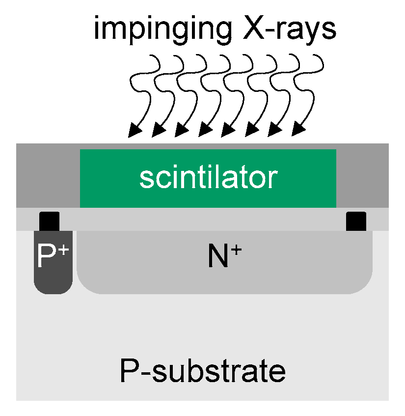
Figure 1 illustrates the structure of N
+/P-sub photodiodes. The X-ray absorption coefficient of silicon is low, with ≈277 electron–hole pairs being created for each 1 keV of absorbed X-ray photons
[19]. One way to overcome this limitation is to use scintillator materials to convert X-ray radiation into visible light so as to generate a significant number of electron–hole pairs in the silicon photodetectors
[19][20][21][22][23][24].
Figure 1. Concept of an X-ray detector based on a N+/P substate photodiode with a scintillation crystal and aluminum coating.
Thallium-doped cesium iodide (CsI(Tl)) is one of the most used materials for scintillating crystals in X-ray imaging
[19][20][21][22][23]. The light yielded by CsI(Tl) presents a scintillation peak at 550 nm (e.g., in the green portion of the spectrum), with a decay constant of 1 μs, and with a spectral range emission between 350 and 725 nm
[19][20][21][22][23].
Silicon photodetectors can be combined with a variety of other scintillation crystals to produce light of different colors for specific applications
[19][24]. For example, NaI(Tl), Y
3Al
5O
12(Ce), CaI
2, CsI:Na, ZnS(Ag), and CaI
2 can be used to yield light at the spectral peaks of 303 nm, 390 nm, 410 nm, 420 nm, 450 nm, respectively
[24].
As also illustrated in
Figure 1, the layer made of scintillating crystal converts the X-ray radiation into visible light
[25]. Scintillating crystals are then used to produce light photons proportional to the amount of X-ray energy absorbed. The yielded light can now be converted into a photocurrent by the photodetector. The aluminum coating is required to prevent the loss of the back-emitted visible light and to prevent crosstalk between individual photodetectors
[19][26].
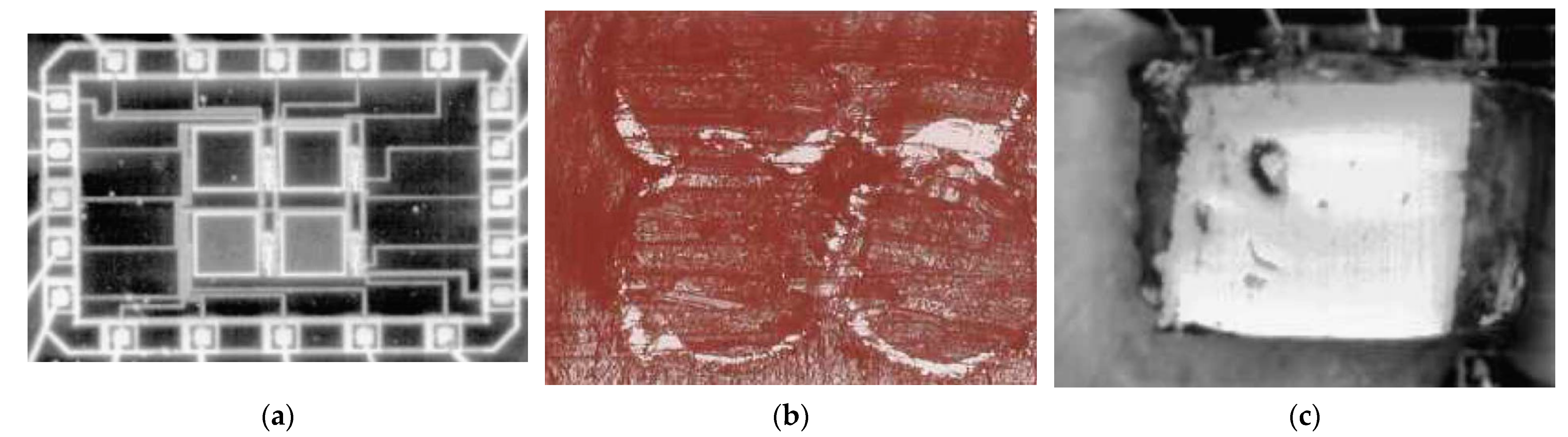
Figure 2 illustrates the final results of several fabrication steps performed by Rocha et al. to present a CMOS X-ray detector proof-of-concept
[19].
Figure 2. For a selected application of an X-ray sensor with an array of 2 × 2 pixels
[19]: photographs (
a) of a CMOS microdevice with an array of 2 × 2 pixels made of N
+/P sub photodiodes before positioning the array of CsI(Tl) scintillators, (
b) of the CsI(Tl) scintillators placed inside the aluminum cavities, and (
c) of the final prototype of the X-ray sensor. These figures were reproduced with previous authorization via Elsevier.
The photograph in
Figure 2a show a CMOS microdevice with an array of 2 × 2 pixels made of N
+/P-sub photodiodes before positioning the array of CsI(Tl) scintillators
[19]. The photograph in
Figure 2b shows CsI(Tl) scintillating crystals filling the aluminum cavities
[19]. After that, the cavities were covered with a thin film of aluminum with a thickness of 10 μm. Finally, the photograph in
Figure 2c shows the final prototype of the X-ray sensor after the cavities covered with the thin film of aluminum were flipped and placed on top of the photodiodes
[19]. The transmissivity of the aluminum with a thickness of 10 μm is relativity low for visible light.
The application of X-ray CMOS detectors is a well-known method and it is being used by several major brands as a cutting-edge technology. Table 3 lists the main characteristics of state-of-the-art research works.
Table 3. Main key characteristics of selected state-of-the-art works.
Alzahrani et al.
[27] presents a new detector branded Lassena (CsI). This detector uses a coupled CsI(Tl) scintillator with a thickness of 1000 µm. This CMOS sensor is also composed of a matrix of 2786 × 2400 pixels in an area of 24 cm × 14 cm, and a pitch of 50 µm. The quantum efficiency is about 50% at 540 nm. The readout electronics contain an ADC with a resolution of 14 bits. This CMOS sensor was characterized by three X-ray beams, e.g., RQA3 with 50 kV, RQA5 with 70 kV and RQA7 with 90 kV. The detector presented linear responses with
R = 99.9% for these exposures: 0.26 to 2.17 μGy for RQA3 and 0.29 to 1 μGy for RQA5 and RQA7.
Desjardins et al.
[28] used a camera equipped with a commercialized backside-illuminated scientific CMOS (sCMOS-BSI) sensor with an array of 2048 × 2048 pixels, a pixel size of 11 × 11 µm per pixel, and a physical size of 22.5 mm × 22.5 mm, creating a four-megapixel sensor, with a pixel pitch of 21 µm. They used a soft X-ray beam with an energy between 30 and 2000 eV to characterize the CMOS sensor, where a quantum efficiency higher than 90% in the lower energy range was observed.
Son et al.
[29] evaluated image quality in radiation therapy using an Elekta iviewGT, a 1024 × 1280 pixel sensor with a size of 41 cm × 41 cm, and a pixel pitch of 172 µm with an image depth of 16 bits. They evaluate the MTF (modulation transfer function), NPS (noise power spectrum), and DQE (detective quantum efficiency), which showed high accuracy in radiation delivery at the spatial frequency in 1.0 mm
−1.
Konstantinidis et al.
[30] used the Dexela 2923 CMOS sensor to acquire X-ray images. The CMOS X-ray sensor comprises an array of 1944 × 1536 pixels with a pixel pitch of 75 µm in a package size of 11.5 cm × 14.5 cm. The performance of the CMOS sensor was evaluated with a Varian RAD-70 with the voltage settled between 28 kV and 70 kV.
Scheuermann et al.
[31] used a Sharp-AMFPI that is composed of an array of 320 × 320 thin-film transistors (TFTs) with an active area of 24 cm × 30 cm with a pixel pitch of 85 µm. The optical performance of their X-ray sensor was characterized with a 30 kVp Mo/Mo beam. The Sharp-AMFPI X-ray sensor was able to achieve an optical avalanche gain of 76 ± 5 at an electric field
ESe up to 105 V.µm
−1, being only limited by the optical spread of the CsI scintillator.
4. Labs-On-a-Chips (LOCs)
Optical CMOS sensors have also been increasingly studied in the area of clinical and biological analysis, due to their high integration rate, low cost, and portability, guaranteeing that the examination can occur at any site, delivering immediate findings
[32][33]. Minas et al. developed an on-chip integrated CMOS optical detection microsystem for spectrophotometric analysis in biological microfluidic systems, through a double-metal, single-polysilicon 1.6 µm N-well CMOS process
[32]. The microsystem is composed of N
+/P-sub photodetectors with an active area of 100 µm × 100 µm and a light-to-frequency converter that integrated a comparator for readout. The photodetector presented a responsivity of 224 mA/W at
λ = 495 nm and 223 mA/W at
λ = 592 nm. This specific wavelength marks the point where the uric acid molecule and total protein exhibit their highest absorption. The mentioned microsystem was created to seamlessly integrate into a biological setup for quantifying biomolecule concentrations in bodily fluids. Its functionality was demonstrated through the accurate measurement of uric acid levels and total protein in urine. The optical system’s sensitivity was 1 kHz/Wm
2 at
λ = 670 nm. The final lab-on-a-chip created by Minas et al. presented a minimum detection capability of 0.5 mg.dL
−1, with an achieved sensitivity of 5 mg.dL
−1 for uric acid and total protein. This sensitivity corresponds to a relative resolution of 3.3%, meeting the requirements for human urine values. Additionally, the lab-on-a-chip successfully measured concentrations of uric acid and total protein while being illuminated by a 200 W halogen lamp source. CMOS integration enabled Minas et al. to develop a device possessing the equivalent reliability and precision of the spectrophotometric automated equipment utilized in state-of-the-art clinical analysis laboratories. Simultaneously, it is portable, cost-effective, provides comfort for the patient, and additional molecules or biological fluids could be considered as potential candidates for the lab-on-a-chip.
Furthermore, also in
[34][35], CMOS photodiodes based on a 0.35 µm process were used. Both present a small size. However, one was applied for the detection of
Staphylococcus aureus [34] and the other for several applications like diagnosing drug discovery
[35]. In their study, Norian et al.
[34] pioneered the use of CMOS technology to integrate all essential functions for quantitative polymerase chain reaction (qPCR) on a lab-on-a-chip platform. These include temperature control, heating, microfluidics, and fluorescence detection. For fluorescence detection, crucial for monitoring PCR progression, Haig et al. employed integrated single-photon avalanche diodes (SPADs) featuring a shallow P
+ region with a diameter of 7.5 μm within an N-well with a 15 μm diameter. Their work showcases how lab-on-a-chip devices can effectively utilize the advanced design capabilities of silicon CMOS foundries. The authors achieved robust identification and quantification of
Staphylococcus aureus using the proposed lab-on-a-chip
[34].
Manaresi et al.
[35] developed an optical sensing system using standard CMOS technology to detect single particles or clusters, allowing the manipulation of over 10,000 cells simultaneously. The authors detected the particles’ presence using CMOS photodiodes with a 2 µm × 17 µm well-junction photodiode placed underneath the 1.2 μm wide gap, implemented with a CMOS APS. The device was optimized for handling eukaryotic cells (such as the lymphocytes found in blood) in the range of 20–30 µm. Manaresi et al. believe that the CMOS device developed has the potential to be an enabling technology for the creation of innovative protocols in cell biology. Its features include the ability to perform multiple experiments on individual cells simultaneously, detect and isolate rare cells in small samples, deliver compounds in a controlled manner to target cells, and investigate real-time cellular responses to chemicals and cell–cell interactions
[35].
CMOS photodiodes have also been applied for other applications, such as
Giardia lamblia imaging
[36] and oxygen sensors
[37], incorporating both into a lab-on-a-chip device. In
[36], Lee et al. demonstrated the use of an OFM device to perform microscopy imaging of cysts and trophozoites of
Giardia lamblia, using a CMOS optical sensor containing a 2D array of 1280 × 1024 square pixels. This enabled the authors to create an autonomous, inexpensive, and highly compact system for water quality analysis and monitoring in resource-limited areas.
In
[37], Shen et al. employed a CMOS image sensor in a portable optical oxygen sensor. The sensor featured an active array size of 3488 × 2616 pixels, each approximately 1.75 µm × 1.75 µm, integrated with an ADC and a gain amplifier. The authors used PtOEP as the oxygen-sensing material. The emission intensities of PtOEP vary for different oxygen concentrations, consequently they alter the current measured by the CMOS sensor. The authors achieved high sensitivity and linearity in the Stern-Volmer analysis, calculated by:
where
I0 and
I are the emission intensities in the absence and presence of oxygen at concentrations of [O
2], respectively, and
KSV is the Stern–Volmer constant. The device demonstrated a sensitivity of the oxygen sensor, represented by the ratio
I0/
I100, of ≈41. This result is comparable to the values of approximately 50 reported by others using an external spectrophotometer. The authors successfully demonstrated the device’s utility, achieving sensitivity comparable to macroscale benchtop sensor systems, all thanks to the utilization of a low-cost CMOS sensor.
Hu et al. developed a CMOS microdevice comprising an array of 16 × 16 photodiode pixels. Each pixel incorporates a PN-junction with a traditional 3-transistor read-out design. The microdevice was manufactured utilizing a commercially accessible CMOS 350 nm four-metal process offered by Austria Micro Systems (AMS)
[38]. The photodiode presented an output of 408 ± 22 mV in dark conditions, had a minimum detection of 50 nW/cm
2, and started to saturate when exposed to 4.9 µW/cm
2 [38]. The researchers integrated the PN-junction photodiode into a paper strip containing three microfluidic channels. They proved the simultaneous detection of potential sepsis biomarkers, glucose, and lactate
[38]. The detection was carried out using absorbance measurements. It used an LED as a light source, located at the top, and the photodiode was located at the bottom of the paper strip. The authors showed that the voltage across the photodiode varies over time for different concentrations of glucose and lactate. Higher concentrations of analytes lead to lower photodiode voltages. They achieved a limit of detection (LOD) of approximately 520 µM for glucose and 110 µM for lactate, determined from three times the standard deviation of the blank signal. While previous biosensors have achieved lower detection limits, this one provides a sufficiently low LOD for the studied metabolites. By combining a cost-effective paper strip with microfluidic channels and a sensitive CMOS photodiode sensor array, they developed a sturdy, portable, and highly affordable biosensor device suitable for diverse diagnostic tests across numerous applications, easily increasing the number of microfluidic channels
[38].
Regarding the other options for labs-on-a-chip, most of them, as presented in
Table 4, present more expensive
[39], lower packaging density
[40], and more complex systems
[41]. The detector presented by Nieuwenhuis et al., presents a low-dimensions detector through a bipolar IC-process
[42]. However, bipolar technology has a lower packaging density and higher cost than CMOS technology
[40].
Table 4. Specifications of optical detectors integrated in labs-on-a-chip.
5. Angular Measurements of Incident Light
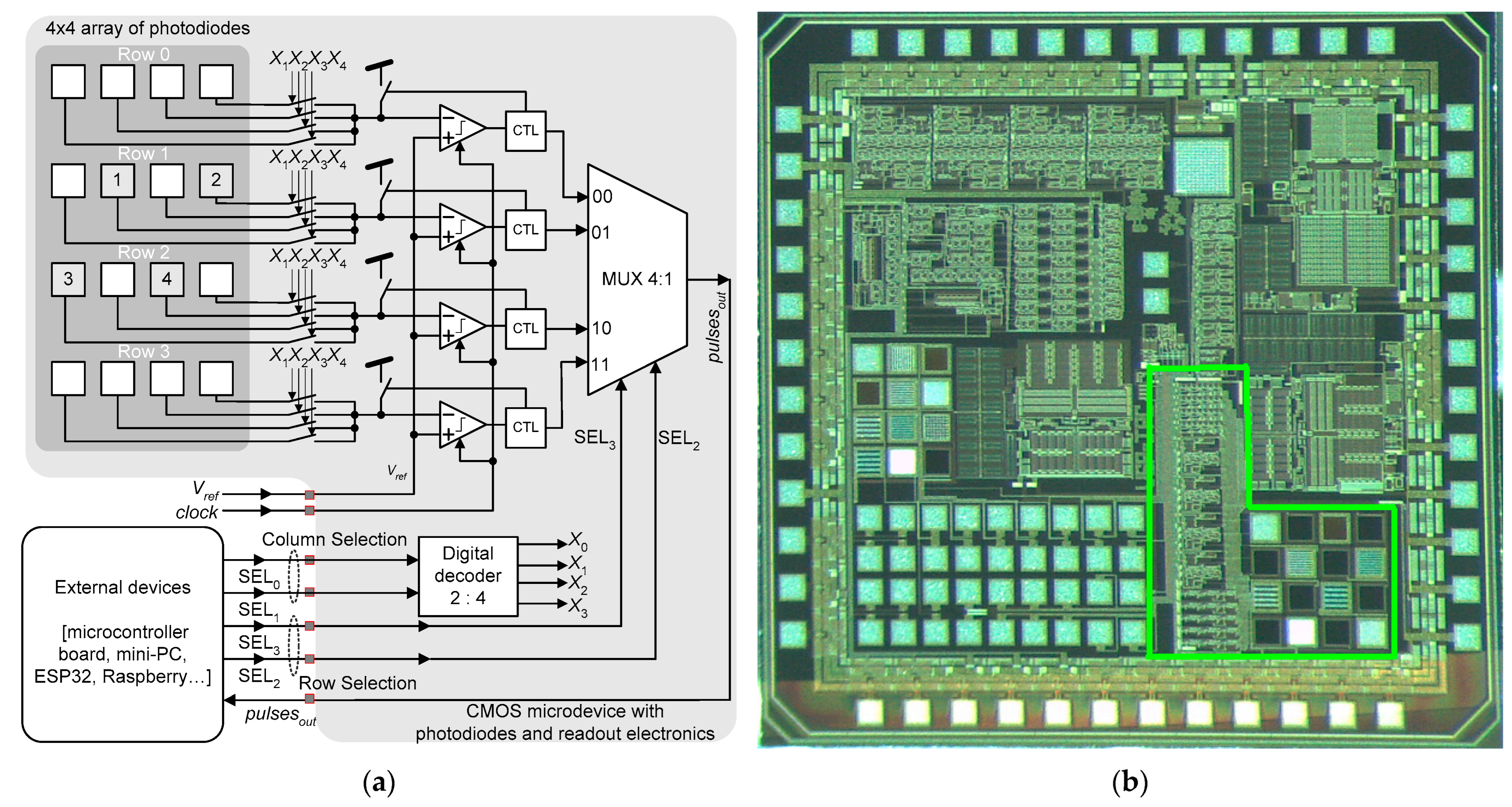
Optical sensors in CMOS can find applications in solar trackers. It is widely known that solar radiation’s angle of incidence is a key factor in determining the size and placement of photovoltaic systems. Solar trackers play a major role when designing the infrastructure and the power output of the panels. Normally, the angle is defined one single time using geographical positioning. However, this technique overlooks local elements like climatic conditions, terrain, and highly reflective buildings that can influence energy production. Costa et al. developed a photovoltaic (PV) sub-module with an optical sensor and readout electronics in a CMOS. The CMOS microdevice was designed to accurately measure the incidence angle of the solar light to automatically track the position of the photovoltaic cells
[46]. The microdevice was fabricated using the 0.7 μm CMOS process from the on semiconductor. This microdevice is composed of an array of 4 × 4 N
+/P-sub photodiodes and the respective readout circuits. As illustrated in
Figure 3a, the photodiodes on a common line share the same current-to-frequency (IV) converter. Each photodiode converts light into pulsed signals. The digital signals SEL
0 and SEL
1 allow only one photodiode on a specific row to connect the IV converter of that row. The signals SEL
2 and SEL
3 select the input of the respective IV converter to connect to the multiplexer output.
Figure 3a illustrates the block diagram of the complete solar tracker, while
Figure 3b shows the photograph of the fabricated microdevice
[46].
Figure 3. (
a) Block diagram of the complete optical sensor developed by Costa et al.
[46], (
b) and the photograph of the fabricated microdevice with details of the solar tracker
[47].
A set of metal microstructures with widths of 5 and 10 μm were created on top of the photodiodes to facilitate the measurements of the impinging light
[46]. Each photodiode generates a response proportional to the angle of incidence. The transduction is based on producing a photocurrent with intensity matching the incoming light according to Equation (1)
[46]. The selected IV converter generates a pulsed signal with a frequency that depends on the intensity of the light that reaches the surface of the respective photodiode.
A prototype of a PV sub-module with this CMOS microdevice was fabricated. The PV sub-module comprises an Arduino Uno board, an Arduino shield with a bus to connect a real time clock (RTC) module, a module with a micro-SD card to store the acquired data, and the CMOS microdevice with the optical sensor
[46]. A box made of acrylonitrile butadiene styrene (ABS) was printed in 3D to enclose and protect the electronic circuits of the PV sub-module against harsh environmental conditions such as weather and dust. An optical attenuator was placed in the light aperture to prevent the saturation of the optical sensor. The PV-sub module measured 12 cm × 10 cm × 4 cm
[46]. A series of initial tests were conducted in the laboratory to obtain the optimal parameters and frequency settings in order to avoid the saturation of the photodiode
[46]. These tests preceded the final evaluation of solar incidence on the roof, where a setup was constructed to measure the angles and the corresponding frequencies of the pulsed signal. The laboratory setup featured a rotating arm with a bright LED at the top and a servomotor fixed at the arm’s lower end. The laboratory setup was placed on top of an optical table to ensure mechanical stabilization against vibrations. The servomotor covered a range of rotation angles from 40° to 150° in steps of 5°, while the LED brightness was directly controlled by a potentiometer. The CMOS microdevice was supplied with a voltage supply of 5 V via the Arduino Uno. The reference voltage
Vref was settled to 2 V and obtained from the voltage supply via a potentiometer. The clock signal, CLK, was adjusted to 50 kHz using the CA4093 gated oscillator. The information about the instantaneous frequency of the signal
pulsesout at the output of microdevice was acquired with the help of a frequency counter.
A second setup was used to track the solar position on the roof
[46]. This configuration involved a servomotor tilting the case containing all of the sensor components, sweeping angles from −90° to +90°. The PV sub-module’s sensor was sensitive to both the east–west and north–south directions, necessitating an additional servomotor to sweep the orthogonal direction. Unlike the laboratory setup, this system rotates the entire case, obtaining frequency measurements for all angles with approximate intervals of two minutes. The second setup was composed of the full PV sub-module, power supply source, and mechanical parts. This setup gave accurate information on the rotation angle without rotating the bulky PV panel. This setup is compact, occupying only 24 cm × 10 cm × 14 cm; thus, it is suitable for limited-space environments
[46].
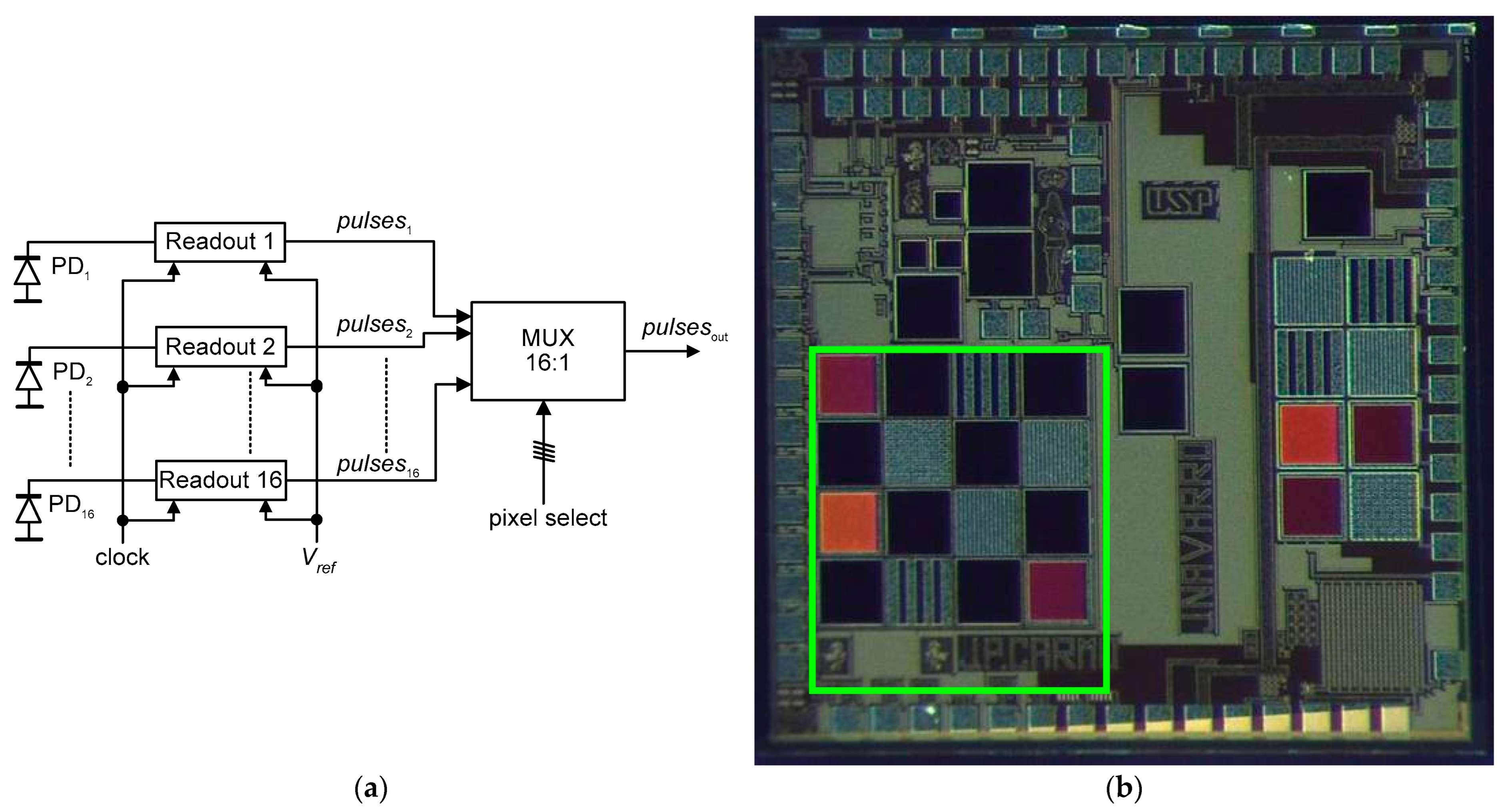
Costa et al. also developed another CMOS microdevice with an optical sensor and respective readout electronics
[48]. This second microdevice is, in part, similar to the one presented in
[46]. The microdevice was fabricated using the 0.18 μm CMOS technology from TSMC and is composed of a matrix of 4 × 4 N
+/P-sub photodiodes, where two photodiodes have 5 μm metal microstructures on top and the other two photodiodes have 20 μm metal microstructures on top
[48]. These metal patterns are intended for coarse and fine angle measuring. Each photodiode has its own current-to-frequency converter, with all working in parallel and producing 16 independent pulsed signals. A set of four digital signals controls a digital multiplexer to select only one of the 16 inputs.
Figure 4a also shows the block diagram of the readout electronics, while
Figure 4b depicts the photograph of the fabricated microdevice
[48]. The measurements, performed on two photodetectors, showed the following behavior
[48]:
where
θ [degree] is the angle of incidence of light. The laboratory setup used a potentiometer to set the reference voltage from the power supply to
Vref = 1.68 V. The clock signal, CLK, was produced using a low-cost commercial arbitrary waveform generator, while a Tektronix digital oscilloscope monitored the signal
pulsesout at the circuit output. A high-power white LED module Thorlabs model MCWHL5 served as the light source. The angle incidence was manually adjusted using a mini-goniometer from Optron featuring scale markings
[48]. The conclusion was that the equations
fPD1(
θ) and
fPD2(
θ) agree well with the measurements (with correlation factors of 97.7% and 94.1%, respectively).
Figure 4. (
a) Block diagram of the complete solar tracker, and (
b) the photograph of the fabricated microdevice with details of the complete solar tracker developed by Costa et al; the area inside the green box comprises the circuit of solar tracker
[48].
Gómez-Merchan et al. introduced a sun sensor architecture that is particularly pertinent due to the rising demands of satellite deployment
[49]. Its design leverages photodiodes in the photovoltaic regime instead of the conventional photoconductive mode, enabling zero power consumption for the photoreceptor and facilitating continuous signal generation with logarithmic compression. Integrated with low-power asynchronous digital circuitry for on-chip region of interest (ROI) centroid computation, the sensor was fabricated using the UMC 0.18 µm technology with dimensions of 1516 µm × 1516 µm, in continuous mode, and 1318 μm × 1318 μm in time-to-first-spike (TFS) mode. Both modes utilize an array of 64 × 64 pixels with a pitch of 19.5 µm, achieving a field of view (FOV) of 88.67° and a resolution of up to 0.98° per pixel. The continuous mode records 5000 measurements per second for 1000 lux, while the TFS mode captures 1000 frames per second. The power consumption is capped at 63 µW for the continuous mode and 1.07 mW for the TFS mode, with both modes boasting a dynamic range higher than 100 dB. The continuous mode resolution stands at 1.23° with an accuracy of 2.37° (latitude) and 5.82° (azimuth), whereas the TFS mode presents a higher resolution of 0.0048° and an accuracy of 0.012° (latitude) and 0.043° (azimuth)
[49].
Chang et al. from the Space System Research Lab (SSRL) at Korea Aerospace University developed a CMOS sun sensor to determine the incident angle of sunlight. This sensor captures sunlight’s projection to calculate the angle
[50]. The design comprises a mask with holes in different configurations and diameters that allow sunlight through, positioned at a fixed distance from the sensor. The mask is made of an opaque material, typically silicon, with black-coated SUS306 prototype masks having different hole configurations. The CMOS sensor used is the MT9M112 model by Micron Technology, Inc., which is smaller and consumes less power than CCD sensors, operating within a range of 90 mW to 160 mW, making it ideal for small satellites. The MT9M112 has a resolution of 1280 × 1024 pixels, measuring 48.35 mm × 83.88 mm × 34.71 mm, and weighing 80.8 g. The digital sun sensor relies on the accurate determination of the projected sunlight’s center on the CMOS for precise measurements
[50].
Romijn et al. introduces a quadrant sun position sensor developed using silicon carbide (SiC) technology, specifically aimed at overcoming the pitfalls of existing silicon-based sensors that inadvertently react to the Earth’s reflected visible light
[51]. This new sensor boasts unique quadrant architecture, consisting of four individual photodetectors arranged strategically. These detectors, when combined with a transparent sapphire optical window, function to cast a light spot, facilitating the calculation of direction vectors to the light source. Operating in a field-of-view of ±33°, this device reaches a minimal mean error of just 1.9°. Furthermore, the tests revealed the sensor’s ability to remain “visible blind”, meaning it can accurately differentiate UV light sources from regular ambient light conditions. The sensor employs a 0.81 cm
2 photodetector, constructed using 4H-SiC technology aimed at the UV spectral range, and utilizes a pre-coated sapphire optical window. The SiC foundation ensures high UV-to-visible selectivity and enhanced radiation toughness, offering potential for integrated on-chip readout electronics
[51]. The same research group developed another sensor constructed from silicon carbide; the sensor integrates wafer-thin 3D optics and boasts a compact design measuring 10 mm × 10 mm × 1 mm
[52]. It delivers a mean angular accuracy of 5.7° within a ±37° field-of-view and is equipped with an on-chip temperature sensor, demonstrating sensitivity from 20 °C to 200 °C. The device operates at a minimal power consumption of ≈60 µW. Its design leverages silicon carbide photodetectors to effectively diminish signal distortions from Earth-reflected light, offering a solution that not only meets satellite miniaturization needs but also anticipates significant cost savings in large-scale production.
Another work by Romijn et al. presents a developed angle-sensitive optical sensor that removes the need for conventional optics
[53]. The sensor’s design integrates CMOS-compatible diffraction grating layers, allowing for both cost-effective fabrication and significant miniaturization. This approach eliminates the necessity for 3D optic post-processing. The sensor is capable of detecting angular information from a monochromatic light source across a single axis with a mean absolute accuracy of 0.6° in a ±26° field-of-view using just four unique pixels. When it comes to fabrication, the CMOS opto-electronic system used in the sensor’s construction leverages in-house BiCMOS technology; a process involving seven lithography masks on 100 mm diameter p-type wafers. Vertical photodetectors, sized at 0.5 mm × 0.5 mm, are utilized, which feature an 8 × 8 pixel array. The device’s angle-sensitive fabrication features a double-diffraction grating stack, which begins with a 2.7 nm oxide layer, followed by layers of titanium nitride (TiN). This TiN layer was chosen due to its low reflectivity properties, which are ideal for the sensor’s function.
Koch et al. engineered a sensor for the continuous detection of incoming light angles, fabricated using a standard 250 nm CMOS technology
[54]. It employs a simplified design with just two diodes; one shaded and one unshaded. These diodes detect the angle based on the distinct photocurrent ratios produced by them. A feature of this sensor is its compactness, occupying a photo-sensitive area of merely 0.285 mm
2, while the entire microdevice spans an area of 1.19 mm
2. The experimental setup of the sensor boasts a precise mechanical construction that can be adjusted to a light source with a remarkable accuracy of one-twelfth of a degree. When evaluating its efficiency, the sensor exhibited accuracy for angles ranging from 0° to 35°. The sensor consumes almost no power when idle and a mere 1 mW during its measurement cycles
[54].
Table 5 compares a selected sample of state-of-the-art solar trackers to finish off this section.
Table 5. Comparison of selected state-of-the-art solar trackers.
| Ref No. |
Fabrication Technology |
Photodiodes, Architecture |
Key Features |
Power
Consumption |
Other
Properties |
Purpose
Finality |
| [46] |
0.7 μm CMOS (on semiconductor) |
4 × 4 array |
Metal microstructures (5 μm, 10 μm) |
265 mW, when supplied
with 5 V. |
Precise solar tracking, scalable design |
Angle of solar light incidence |
| [48] |
0.18 μm CMOS (TSMC) |
4 × 4 array |
Metal microstructures (5 μm, 20 μm) |
Not mentioned |
Similar to [46][55], with modified tech/design |
Angle of solar light incidence |
| [49] |
UMC 0.18 µm |
64 × 64 pixel |
Pinhole |
63 µW–1.07 mW |
FOV: 88.67°, Resolution: up to 0.98°/pixel |
Sun sensor for satellite deployment |
| [50] |
Not mentioned (MT9M112 by Micron Technology) |
Not mentioned |
Mask with different hole configurations |
90–160 mW |
Resolution: 1280 × 1024 pixels, Weight: 80.83 g |
Determines angle of sunlight |
| [51] |
4H-SiC |
Quadrant 2 × 2 photodetectors |
Transparent sapphire optical window |
Not mentioned |
FOV: ±33°,
Error: 1.9° |
Differentiates UV from ambient light |
| [52] |
6 μm 4H–SiC CMOS technology |
Not mentioned |
Wafer-thin 3D optics |
Approx ±60 µW |
FOV: ±37°,
Accuracy: 5.7° |
Satellite attitude control |
| [53] |
BICMOS |
8 × 8 pixel array |
Double diffraction grating stack |
Not mentioned |
FOV: ±26°,
Accuracy: 0.6° |
Detects angular information |
| [54] |
250 nm CMOS |
Two diodes (shaded unshaded) |
Photocurrent ratios |
Nearly 0 to 1 mW |
Angle Range: ±85°,
high resolution |
Continuous detection of light angles |
 +1 credit