Submitted Successfully!
To reward your contribution, here is a gift for you: A free trial for our video production service.
Thank you for your contribution! You can also upload a video entry or images related to this topic.
Version Summary Created by Modification Content Size Created at Operation
1 -- 1840 2024-02-26 07:30:30 |
2 layout Meta information modification 1840 2024-02-26 07:47:43 |

Video Upload Options

Do you have a full video?

Confirm

Are you sure to Delete?
Cite
If you have any further questions, please contact Encyclopedia Editorial Office.
Butt, M.A. Nuanced Concept of the Evanescent Field Ratio. Encyclopedia. Available online: https://encyclopedia.pub/entry/55427 (accessed on 18 May 2024).
Butt MA. Nuanced Concept of the Evanescent Field Ratio. Encyclopedia. Available at: https://encyclopedia.pub/entry/55427. Accessed May 18, 2024.
Butt, Muhammad A.. "Nuanced Concept of the Evanescent Field Ratio" Encyclopedia, https://encyclopedia.pub/entry/55427 (accessed May 18, 2024).
Butt, M.A. (2024, February 26). Nuanced Concept of the Evanescent Field Ratio. In Encyclopedia. https://encyclopedia.pub/entry/55427
Butt, Muhammad A.. "Nuanced Concept of the Evanescent Field Ratio." Encyclopedia. Web. 26 February, 2024.
Nuanced Concept of the Evanescent Field Ratio
Edit

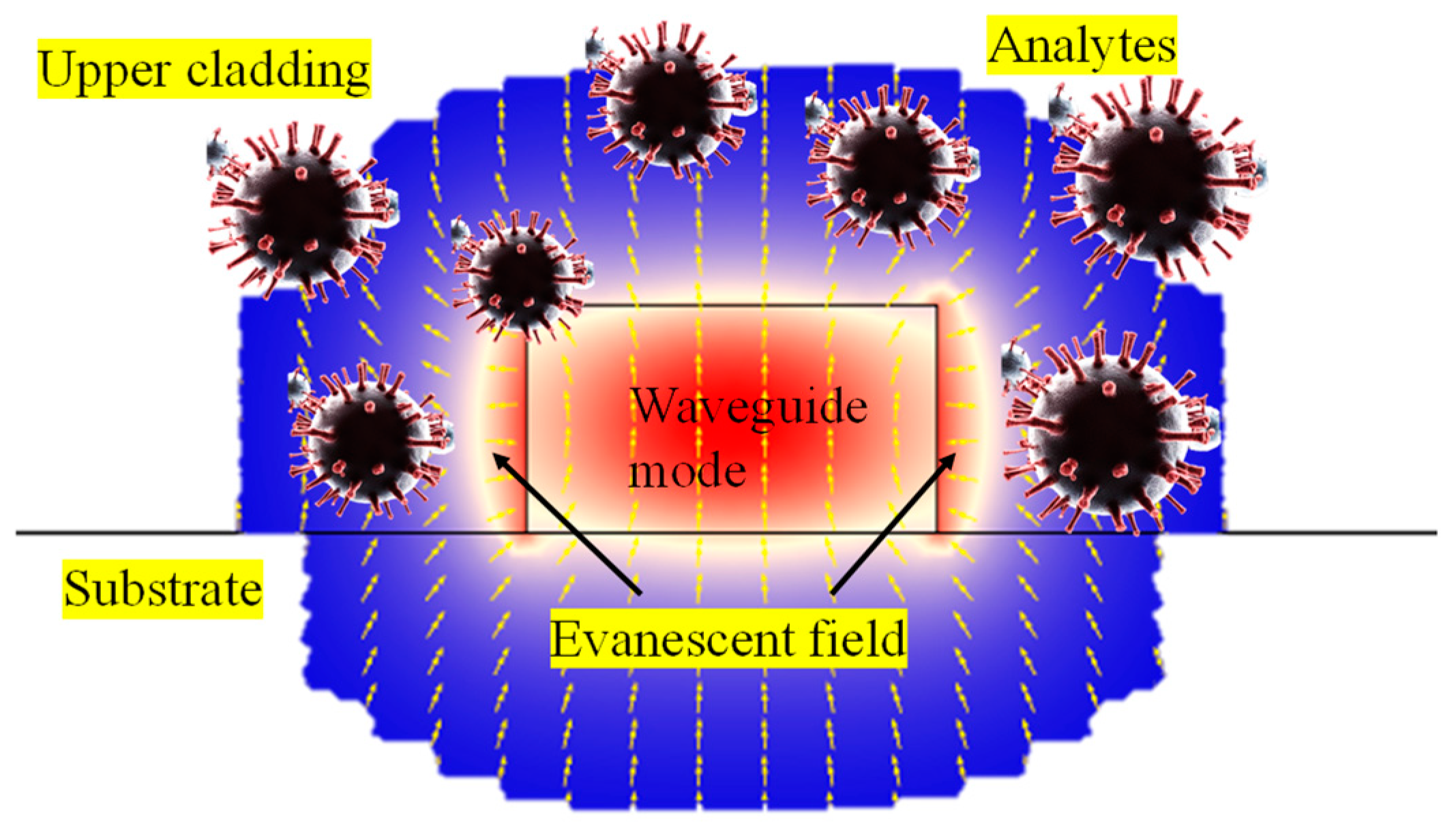
Photonic sensors utilize light–matter interaction to detect physical parameters accurately and efficiently. They exploit the interaction between photons and matter, with light propagating through an optical waveguide, creating an evanescent field beyond its surface. This field interacts with the surrounding medium, enabling the sensitive detection of changes in the refractive index or nearby substances. By modulating light properties like intensity, wavelength, or phase, these sensors detect target substances or environmental changes. Advancements in this technology enhance sensitivity, selectivity, and miniaturization, making photonic sensors invaluable across industries. Their ability to facilitate sensitive, non-intrusive, and remote monitoring fosters the development of smart, connected systems. 

evanescent field photonic sensor optical waveguide light–matter interaction

1. Introduction

Photonic sensors based on optical waveguides (WGs) operate at the forefront of cutting-edge technology, leveraging the fundamental principle of guided light propagation to establish a sophisticated mechanism for exceptionally sensitive and specific environmental monitoring [1][2]. Photonic sensors based on evanescent field principles represent a sophisticated and versatile class of optical sensing devices [3]. These sensors exploit the evanescent field, an electromagnetic wave that extends just beyond the surface of a material, to detect changes in the surrounding environment. In these systems, light is typically coupled into a WG or optical fiber, permitting the evanescent field to interact with the adjacent medium. The interaction induces alterations in the transmitted light, such as changes in intensity or wavelength, which are then precisely assessed. This modulation in the optical signal serves as a sensitive indicator for variations in the targeted parameters, such as refractive index, temperature, or the presence of specific biomolecules. Photonic sensors based on evanescent field principles find applications in a myriad of fields, ranging from biochemistry and medical diagnostics to environmental monitoring and industrial sensing [4][5][6]. Their high sensitivity, real-time monitoring capabilities, and non-invasive nature make them vital tools for progressing our capabilities in precision sensing and measurement technologies.
Optical WG biochemical sensing represents a convergence of optical WG technology with biological and chemical methodologies. Within the realm of chemical sensors, biosensors specifically play a pivotal role in this interdisciplinary field. Optical biochemical sensing can be categorized into labeled and unlabeled approaches, with refractive index sensing being an example of the latter. In the context of optical WG biochemical sensors, alterations in the evanescent field induced by changes in parameters like the refractive index and absorption coefficient occur. Typically, these changes stem from variations in the phase of transmitted light, leading to a distinct effective refractive index in the optical transmission mode. The mode coupling theory, applicable to sensors like surface plasmon resonance (SPR) and grating sensors, is employed to calculate the resultant change in the effective refractive index [7][8][9]. This calculation method extends to devices such as microring resonators (MRRs) [10][11], Mach–Zehnder interferometers (MZIs) [12], multimode interferences (MMIs) [13][14], fiber Bragg gratings [15], photonic crystals [16], and other differential interferometers [17].
Utilizing the refractive index change or absorption spectrum, optical WG refractive index biochemical sensors enable qualitative or quantitative analyses of gases, liquids, and solid substances in testing scenarios. Beyond that, these sensors find applications in detecting harmful gas concentrations in the environment, monitoring food and water quality, and identifying bacteria and viruses for public health concerns and chemical threat perception [8]. The label-free detection mechanism employed by biochemical sensors relies on the change in the refractive index caused by molecular interactions. This approach is particularly advantageous for measuring chemical substances, viruses, or bacteria, as it is directly correlated with the target sample concentration or surface density. Notably, this method is both cost-effective and straightforward, making it a valuable tool in various analytical applications [18].
Integrated photonic sensors offer numerous advantages in various applications. One significant advantage is their compact size, allowing for easy integration into small devices and systems. They also exhibit high sensitivity and accuracy, making them suitable for precise measurements in fields such as biomedical sensing, environmental monitoring, and telecommunications [2][19]. Additionally, integrated photonic sensors typically have low power consumption, enabling prolonged operation without frequent battery changes or recharging. However, these sensors also come with certain disadvantages. Fabrication processes can be complex and expensive, limiting their accessibility to some researchers and industries [20]. Furthermore, their performance may be susceptible to environmental factors such as temperature fluctuations and mechanical vibrations, requiring additional measures for robustness and reliability. Despite these drawbacks, ongoing research and advancements continue to address these challenges, paving the way for the wider adoption of integrated photonic sensors in diverse applications.

2. Concept of Evanescent Field Ratio

The evanescent field of a mode propagating in a WG is a crucial concept in the study of electromagnetic waves and their behavior within confined structures. The evanescent field refers to the portion of the electromagnetic field that extends beyond the core of the WG into the surrounding medium. Unlike the propagating field, which carries energy along the WG axis, the evanescent field decays exponentially as it moves away from the core [21]. This phenomenon arises due to the total internal reflection of the mode within the WG, causing the electromagnetic field to extend into the adjacent medium. The evanescent field plays a crucial role in various applications, including sensing and WG-based devices, where interactions with the surrounding medium or nearby structures are essential for functionality [22][23][24]. A graphical illustration of the evanescent field of the WG mode interacting with the ambient medium is shown in Figure 1. Understanding and manipulating the evanescent field is fundamental for optimizing the performance of such devices [25].
Figure 1. Illustration of the WG evanescent field interacting with the analytes in the ambient medium.
The evanescent field ratio (EFR) is a parameter that characterizes the strength of the evanescent field compared to the total field in a WG. It is particularly significant in the study of guided electromagnetic modes, such as those in optical fibers or other confined structures. The EFR is calculated by determining the proportion of the total field that comprises the evanescent field. Mathematically, it is expressed as the square of the amplitude of the evanescent field divided by the square of the amplitude of the total field. This ratio provides insights into the extent to which the electromagnetic energy associated with a mode is confined within the WG core and the degree to which it penetrates the surrounding medium. A higher EFR indicates a more pronounced influence of the evanescent field, which is crucial in applications such as sensing, where interactions with the external environment play a vital role in device performance [26][27]. Researchers often use numerical simulations or experimental techniques to measure and analyze the EFR in practical WG configurations [28].

3. Deciphering Evanescent Wave Patterns in Diverse WG Geometries

Rib WGs, ridge WGs, and slot WGs are different types of optical WGs, and their properties, including the characteristics of the evanescent field, can vary. Rib WGs typically consist of a thin strip (rib) of high-refractive-index material on a lower-refractive-index substrate. The evanescent field in rib WGs is generally confined within the high-index region of the WG. The field extends into the cladding but is typically more localized compared to other types of WGs. Ridge WGs have a raised section (ridge) on the WG core, which helps in confining and guiding light. Like rib WGs, the evanescent field in ridge WGs is primarily localized within the high-index region. The dimensions of the ridge can affect the characteristics of the evanescent field. The normalized E-field distribution in a standard ridge WG determined by the finite-element method (FEM) is shown in Figure 2a.
Figure 2. Normalized E-field distribution in the WG geometry at an operational wavelength of 1550 nm: (a) ridge WG of dimensions W × H = 450 nm × 250 nm, (b) slot WG of dimensions W × H = 270 nm × 250 nm and a gap = 50 nm, (c) modified ridge WG geometry of dimensions W × H = 450 nm × 250 nm with a 25 nm buffer layer between gold layer and WG core.
Whereas slot WGs consist of a low-index region (slot) between two high-index regions [29], these WGs are designed to have a substantial part of the optical field concentrated in the low-index slot region as shown in Figure 2b. This design allows for strong light–matter interactions in the slot, making them advantageous for applications such as sensing [4]. While rib and ridge WGs primarily confine the evanescent field within the high-index regions, slot WGs intentionally utilize a low-index slot to enhance the interaction between light and the surrounding medium. The choice of WG depends on the specific requirements of the application, such as the desired level of confinement, interaction strength, and the nature of the surrounding medium.
In [26], Butt et al. proposed a novel metal-assisted silicon strip WG configuration aimed at enhancing the EFR, thereby making it suitable for highly sensitive sensor applications. The metal-assisted WG structure incorporates a thin SiO2 layer positioned between the gold layer and the silicon strip WG. The mode in the metal-assisted silicon strip WG is heightened, leading to an approximately 10% increase in power within the upper cladding, while the power in the substrate experiences a reduction of approximately 5%. The normalized E-field distribution in the metal-assisted silicon strip WG is shown in Figure 2c. These results showcase a significant improvement in the evanescent field within the upper cladding region of a straight strip WG, positioning it as an ideal choice for gas absorption sensors relying on evanescent field interactions.
The subwavelength grating (SWG) WG is recognized for its ability to enhance the evanescent field, a crucial feature in various optical applications [30]. By leveraging periodic structures with dimensions smaller than the wavelength of the guided light, subwavelength gratings facilitate strong coupling between guided modes and the surrounding medium. This design leads to a significant increase in the penetration depth of the evanescent field beyond the WG core. The subwavelength grating’s unique geometric configuration allows for fine-tuning of the effective refractive index and dispersion characteristics, providing engineers with a versatile tool to tailor the evanescent field’s strength and distribution [31]. This enhanced evanescent field is particularly advantageous in applications such as sensing, where interactions with the surrounding environment play a critical role. The subwavelength grating WG’s capability to amplify the evanescent field opens up new possibilities for achieving heightened sensitivity and improved performance in optical devices [32][33][34].
In addition to dielectric waveguides, another type of optical waveguide that facilitates strong light–matter interaction through a high evanescent field is a plasmonic WG [35]. These WGs are designed to guide SPPs, which are collective oscillations of electrons coupled to photons at a metal–dielectric interface. The widely deployed plasmonic WGs for sensing applications are metal–insulator–metal (MIM) WG [36], insulator–metal–insulator (IMI) WG [37], wedge SPP WG [38][39], metallic strip [40][41], etc. The evanescent field in plasmonic WGs extends into the surrounding medium, allowing for strong light–matter interactions in the adjacent regions. This property is particularly advantageous for applications such as sensing, where the evanescent field can be used to probe changes in the refractive index or absorbance of the surrounding medium. Other types of WGs, such as dielectric or photonic crystal WGs, may also offer high evanescent fields depending on their specific design parameters and configurations [16][42][43]. However, plasmonic WGs are often specifically engineered to enhance the evanescent field and enable efficient light–matter interactions in their vicinity.

References

  1. Butt, M.A.; Kazanskiy, N.L.; Khonina, S.N.; Voronkov, G.S.; Grakhova, E.P.; Kutluyarov, R.V. A Review on Photonic Sensing Technologies: Status and Outlook. Biosensors 2023, 13, 568.
  2. Ghosh, S.; Dar, T.; Viphavakit, C.; Pan, C.; Kejalakshmy, N.; Rahman, B.M.A. Compact Photonic SOI Sensors. In Computational Photonic Sensors; Hameed, M.F.O., Obayya, S., Eds.; Springer International Publishing: Cham, Switzerland, 2019; pp. 343–383. ISBN 978-3-319-76556-3.
  3. Vlk, M.; Datta, A.; Alberti, S.; Yallew, H.D.; Mittal, V.; Murugan, G.S.; Jágerská, J. Extraordinary evanescent field confinement waveguide sensor for mid-infrared trace gas spectroscopy. Light Sci. Appl. 2021, 10, 26.
  4. Butt, M.A.; Piramidowicz, R. Standard slot waveguide and double hybrid plasmonic waveguide configurations for enhanced evanescent field absorption methane gas sensing. Photonics Lett. Pol. 2022, 14, 10–12.
  5. Butt, M.A.; Degtyarev, S.A.; Khonina, S.N.; Kazanskiy, N.L. An evanescent field absorption gas sensor at mid-IR 3.39 μm wavelength. J. Mod. Opt. 2017, 64, 1892–1897.
  6. Tai, H.; Tanaka, H.; Yoshino, T. Fiber-optic evanescent-wave methane-gas sensor using optical absorption for the 3.392-μm line of a He–Ne laser. Opt. Lett. 1987, 12, 437–439.
  7. Butt, M.A.; Kazanskiy, N.L.; Khonina, S.N. Tapered waveguide mode converters for metal-insulator-metal waveguide plasmonic sensors. Measurement 2023, 211, 112601.
  8. Liu, C.; Wang, J.; Wang, F.; Su, W.; Yang, L.; Lv, J.; Fu, G.; Li, X.; Liu, Q.; Sun, T.; et al. Surface plasmon resonance (SPR) infrared sensor based on D-shape photonic crystal fibers with ITO coatings. Opt. Commun. 2020, 464, 125496.
  9. Singh, S.; Chaudhary, B.; Upadhyay, A.; Sharma, D.; Ayyanar, N.; Taya, S.A. A review on various sensing prospects of SPR based photonic crystal fibers. Photonics Nanostruct. Fundam. Appl. 2023, 54, 101119.
  10. Kazanskiy, N.L.; Khonina, S.N.; Butt, M.A. A Review of Photonic Sensors Based on Ring Resonator Structures: Three Widely Used Platforms and Implications of Sensing Applications. Micromachines 2023, 14, 1080.
  11. Butt, M.A.; Shahbaz, M.; Piramidowicz, R. Racetrack Ring Resonator Integrated with Multimode Interferometer Structure Based on Low-Cost Silica–Titania Platform for Refractive Index Sensing Application. Photonics 2023, 10, 978.
  12. Vogelbacher, F.; Kothe, T.; Muellner, P.; Melnik, E.; Sagmeister, M.; Krat, J.; Hainberger, R. Waveguide Mach-Zehnder Biosensor with Laser Diode Pumped Integrated Single-Mode Silicon Nitride Organic Hybrid Solid-State Laser. Biosens. Bioelectron. 2022, 197, 113816.
  13. Kribich, K.R.; Copperwhite, R.; Barry, H.; Kolodziejczyk, B.; Sabattié, J.-M.; O’Dwyer, K.; MacCraith, B.D. Novel chemical sensor/biosensor platform based on optical multimode interference (MMI) couplers. Sens. Actuators B Chem. 2005, 107, 188–192.
  14. Elsayed, M.Y.; Sherif, S.M.; Aljaber, S.A.; Swillam, M.A. Integrated Lab-on-a-Chip Optical Biosensor Using Ultrathin Silicon Waveguide SOI MMI Device. Sensors 2020, 20, 4955.
  15. Chen, S.; Zhang, C.; Wang, J.; Li, N.; Song, Y.; Wu, H.; Liu, Y. A Fiber Bragg Grating Sensor Based on Cladding Mode Resonance for Label-Free Biosensing. Biosensors 2023, 13, 97.
  16. Gowdhami, D.; Balaji, V.R.; Murugan, M.; Robinson, S.; Hegde, G. Photonic crystal based biosensors: An overview. ISSS J. Micro Smart Syst. 2022, 11, 147–167.
  17. Hoppe, N.; Scheck, P.; Sweidan, R.; Diersing, P.; Rathgeber, L.; Vogel, W.; Riegger, B.; Southan, A.; Berroth, M. Silicon Integrated Dual-Mode Interferometer with Differential Outputs. Biosensors 2017, 7, 37.
  18. Peng, C.; Yang, C.; Zhao, H.; Liang, L.; Zheng, C.; Chen, C.; Qin, L.; Tang, H. Optical Waveguide Refractive Index Sensor for Biochemical Sensing. Appl. Sci. 2023, 13, 3829.
  19. Altug, H.; Oh, S.-H.; Maier, S.A.; Homola, J. Advances and applications of nanophotonic biosensors. Nat. Nanotechnol. 2022, 17, 5–16.
  20. Butt, M.A. Integrated Optics: Platforms and Fabrication Methods. Encyclopedia 2023, 3, 824–838.
  21. Canning, J.; Padden, W.; Boskovic, D.; Naqshbandi, M.; de Bruyn, H.; Crossley, M.J. Manipulating and controlling the evanescent field within optical waveguides using high index nanolayers . Opt. Mater. Express 2011, 1, 192–200.
  22. Consani, C.; Ranacher, C.; Tortschanoff, A.; Grille, T.; Irsigler, P.; Jakoby, B. Evanescent-Wave Gas Sensing Using an Integrated Thermal Light Source. Proceedings 2017, 1, 550.
  23. Punjabi, N.; Satija, J.; Mukherji, S. Evanescent Wave Absorption Based Fiber-Optic Sensor—Cascading of Bend and Tapered Geometry for Enhanced Sensitivity. In Sensing Technology: Current Status and Future Trends III; Mason, A., Mukhopadhyay, S.C., Jayasundera, K.P., Eds.; Smart Sensors, Measurement and Instrumentation; Springer International Publishing: Cham, Switzerland, 2015; pp. 25–45. ISBN 978-3-319-10948-0.
  24. Schmitt, K.; Oehse, K.; Sulz, G.; Hoffmann, C. Evanescent field Sensors Based on Tantalum Pentoxide Waveguides—A Review. Sensors 2008, 8, 711–738.
  25. Kumar, S.; Kumari, A.; Pradhan, B. Analysis of evanescent field of TE and TM mode in the grounded slab metamaterial waveguide structure. Optik 2015, 126, 3706–3712.
  26. Butt, M.A.; Khonina, S.N.; Kazanskiy, N.L. Enhancement of evanescent field ratio in a silicon strip waveguide by incorporating a thin metal film. Laser Phys. 2019, 29, 076202.
  27. Khonina, S.N.; Kazanskiy, N.L.; Butt, M.A. Evanescent Field Ratio Enhancement of a Modified Ridge Waveguide Structure for Methane Gas Sensing Application. IEEE Sens. J. 2020, 20, 8469–8476.
  28. Consani, C.; Dubois, F.; Auböck, G. Figures of merit for mid-IR evanescent-wave absorption sensors and their simulation by FEM methods. Opt. Express 2021, 29, 9723–9736.
  29. Ranacher, C.; Consani, C.; Jannesari, R.; Grille, T.; Jakoby, B. Numerical Investigations of Infrared Slot Waveguides for Gas Sensing. Proceedings 2018, 2, 799.
  30. Torrijos-Morán, L.; Griol, A.; García-Rupérez, J. Experimental study of subwavelength grating bimodal waveguides as ultrasensitive interferometric sensors. Opt. Lett. 2019, 44, 4702–4705.
  31. Kazanskiy, N.L.; Khonina, S.N.; Butt, M.A. Subwavelength Grating Double Slot Waveguide Racetrack Ring Resonator for Refractive Index Sensing Application. Sensors 2020, 20, 3416.
  32. Sun, Y.; Hu, G.; Cui, Y. Subwavelength grating waveguide racetrack-based refractive index sensor with improved figure of merit. Appl. Opt. 2020, 59, 10613–10617.
  33. Awasthi, K.; Malviya, N.; Kumar, A. Silicon Subwavelength Grating Slot Waveguide based Optical Sensor for Label Free Detection of Fluoride Ion in Water. IETE Tech. Rev. 2023, 1–12.
  34. Butt, M.A.; Tyszkiewicz, C.; Wojtasik, K.; Karasiński, P.; Kaźmierczak, A.; Piramidowicz, R. Subwavelength Grating Waveguide Structures Proposed on the Low-Cost Silica–Titania Platform for Optical Filtering and Refractive Index Sensing Applications. Int. J. Mol. Sci. 2022, 23, 6614.
  35. Kazanskiy, N.L.; Khonina, S.N.; Butt, M.A. Plasmonic sensors based on Metal-insulator-metal waveguides for refractive index sensing applications: A brief review. Phys. E Low-Dimens. Syst. Nanostruct. 2020, 117, 113798.
  36. Kwon, M.-S. Metal-Insulator-Silicon-Insulator-Metal Waveguides Compatible with Standard CMOS Technology. Opt. Express 2011, 19, 8379–8393.
  37. Lembrikov, B.I.; Ianetz, D.; Ben-Ezra, Y. Metal/Insulator/Metal (MIM) Plasmonic Waveguide Containing a Smectic a Liquid Crystal (SALC) Layer. In Proceedings of the 19th International Conference on Transparent Optical Networks (ICTON), Girona, Spain, 2–6 July 2017; Available online: https://ieeexplore.ieee.org/document/8024834 (accessed on 18 February 2024).
  38. Bian, Y.; Zheng, Z.; Liu, Y.; Liu, J.; Zhu, J.; Zhou, T. Hybrid wedge plasmon polariton waveguide with good fabrication-error-tolerance for ultra-deep-subwavelength mode confinement. Opt. Express 2011, 19, 22417–22422.
  39. Zhang, Z.; Wang, J. Long-range hybrid wedge plasmonic waveguide. Sci. Rep. 2014, 4, 6870.
  40. Gao, L.; Tang, L.; Hu, F.; Guo, R.; Wang, X.; Zhou, Z. Active metal strip hybrid plasmonic waveguide with low critical material gain. Opt. Express 2012, 20, 11487–11495.
  41. Kong, G.S.; Ma, H.F.; Cai, B.G.; Cui, T.J. Continuous leaky-wave scanning using periodically modulated spoof plasmonic waveguide. Sci. Rep. 2016, 6, 29600.
  42. Scullion, M.G.; Di Falco, A.; Krauss, T.F. Slotted photonic crystal cavities with integrated microfluidics for biosensing applications. Biosens. Bioelectron. 2011, 27, 101–105.
  43. Butt, M.A.; Khonina, S.N.; Kazanskiy, N.L. Recent advances in photonic crystal optical devices: A review. Opt. Laser Technol. 2021, 142, 107265.
More
Information
Subjects: Optics
Contributor MDPI registered users' name will be linked to their SciProfiles pages. To register with us, please refer to https://encyclopedia.pub/register :
View Times: 54
Revisions: 2 times (View History)
Update Date: 26 Feb 2024
1000/1000