Submitted Successfully!
To reward your contribution, here is a gift for you: A free trial for our video production service.
Thank you for your contribution! You can also upload a video entry or images related to this topic.
Version Summary Created by Modification Content Size Created at Operation
1 -- 8934 2024-02-25 09:19:51 |
2 Reference format revised. + 98 word(s) 9032 2024-02-26 01:40:56 | |
3 remove blank line Meta information modification 9032 2024-02-29 08:25:34 |

Video Upload Options

Do you have a full video?

Confirm

Are you sure to Delete?
Cite
If you have any further questions, please contact Encyclopedia Editorial Office.
Abbas, M.; Xu, X.; Rauf, M.; Kyaw, A.K.K. Defects-Induced Voltage Losses of Perovskite Solar Cells. Encyclopedia. Available online: https://encyclopedia.pub/entry/55411 (accessed on 28 April 2024).
Abbas M, Xu X, Rauf M, Kyaw AKK. Defects-Induced Voltage Losses of Perovskite Solar Cells. Encyclopedia. Available at: https://encyclopedia.pub/entry/55411. Accessed April 28, 2024.
Abbas, Mazhar, Xiaowei Xu, Muhammad Rauf, Aung Ko Ko Kyaw. "Defects-Induced Voltage Losses of Perovskite Solar Cells" Encyclopedia, https://encyclopedia.pub/entry/55411 (accessed April 28, 2024).
Abbas, M., Xu, X., Rauf, M., & Kyaw, A.K.K. (2024, February 25). Defects-Induced Voltage Losses of Perovskite Solar Cells. In Encyclopedia. https://encyclopedia.pub/entry/55411
Abbas, Mazhar, et al. "Defects-Induced Voltage Losses of Perovskite Solar Cells." Encyclopedia. Web. 25 February, 2024.
Defects-Induced Voltage Losses of Perovskite Solar Cells
Edit

The power conversion efficiency (PCE) of single-junction perovskite solar cells (PSCs) has reached 26.1% in small-scale devices. However, defects at the bulk, surface, grain boundaries, and interfaces act as non-radiative recombination centers for photogenerated electron-hole pairs, limiting the open-circuit voltage and PCE below the Shockley–Queisser limit. These defect states also induce ion migration towards interfaces and contribute to intrinsic instability in PSCs, reducing the quasi-Fermi level splitting and causing anomalous hysteresis in the device. The influence of defects becomes more prominent in large-area devices, demonstrating much lower PCE than the lab-scale devices. Therefore, commercializing PSCs faces a big challenge in terms of rapid decline in working performance due to these intrinsic structural defects.

Perovskite solar cells ionic defects power conversion efficiency grain boundaries open circuit voltage

1. Introduction

Perovskite solar cells (PSCs) based on organic-inorganic metal halide perovskites have achieved a certified power conversion efficiency (PCE) of 26.1% just a decade after research efforts began. This remarkable success exceeds the efficiency of other well-developed thin-film photovoltaic technologies, such as copper indium gallium selenide (CIGS) or cadmium telluride (CdTe) in small-area devices (<1 cm2) [1]. The outstanding optoelectronic properties of perovskites (large absorption coefficient, long carriers diffusion length, tunable band gap, etc.) [2][3][4], their low-cost and abundance in the earth [5][6][7], and their ease of fabrication through low-temperature solution deposition technologies [8] make PSCs highly attractive for commercialization. It is expected that PCE of PSCs will surpass that of single crystalline silicon solar cells (26.7%) [9] in the near future, making them a highly efficient renewable energy source that could replace fossil fuels [10]. However, the current PCE is still lower than the theoretically calculated value based on the energy bandgap of perovskites (1.48–1.6 eV). Furthermore, the rapid decrease in PCE when operating in ambient air remains a significant challenge in achieving the minimum twenty-year operation lifetime required for the commercialization of a solar cell technology [11][12][13][14]. The PCE being lower than the Shockley–Queisser (SQ) limit and the unstable photovoltaic performance of PSCs are both primarily caused by defects in the polycrystalline perovskite layer during its solution fabrication [15][16][17][18][19].
Due to the soft ionic nature of perovskites, defects are inevitably produced in a disorderly manner during the crystallization process. The low formation energy of perovskite is a primary reason for the generation of point defects [7][20][21] that are readily produced on the surface and along the grain boundaries (GBs). These defects act as trap states for photogenerated electrons and holes, limiting the performance of the device. Most of the defects formed in perovskite materials are shallow-level defect states with low formation energies and negligible contribution to non-radiative recombination, allowing perovskites to exhibit high defect tolerance, as explained by their long diffusion lengths [22]. However, these defects can alter the energy level alignment of the active layer with adjacent carrier transport layers. Moreover, charged point defects can migrate to interfaces as the ionic defects in perovskite film provide a pathway for their movement by creating an electric field. The accumulated ions at the interfaces adversely affect the charge collection of the device, resulting in current density-voltage (J-V) hysteresis [23][24][25][26]. Moisture instability is also related to interfacial defects as oxygen or water molecules penetrate the perovskite layer through these defects and induce its degradation. Deep-level bulk defects are produced under high-temperature growth conditions and are also accountable for suppressing PCE and device stability. Many reports confirm that the improvement in open-circuit voltage (VOC) and fill factor (FF) are directly related to the passivation of defect states in PSCs. Therefore, it is essential to passivate both deep-level and shallow-level defects to enhance device performance and improve stability.
Numerous effective defect passivation techniques, including compositional engineering [27], additive engineering [28], post-surface treatments [29], dimensionality engineering [30], and interlayer engineering [31] have been reported in recent years to improve the stability and PCE of PSCs [32][33][34][35][36][37]. Mixed cations and anions compositions can tune bandgap, eliminate phase instability, and increase carrier lifetime by limiting the formation of bulk defects. A-site doping with a small amount of alkali metal cations can effectively stabilize the pure perovskite phase and eliminate hysteresis by suppressing the bulk defects (ion vacancies, interstitial ions, etc.) and surface or GBs defects [38][39][40][41].
Surface defects are known to be a significant source of non-radiative recombination centers and can easily form during the thin film crystallization process. Passivating agents such as Lewis acids and bases [27][42], long-chain polymers [43], hydrophobic molecules [44], and wide bandgap oxygen-containing lead salts [45] can be used to passivate these surface defects. For example, thiophene derivatives containing Lewis acid-base functional groups are widely reported to enhance charge transfer and collection at the interface while passivating surface defects with their highly delocalized π-electrons [46]. The passivation of interfacial defects by forming a layered two-dimensional (2D) perovskite on the top surface of a three-dimensional (3D) perovskite remarkably improves the stability and performance of PSCs. The 2D layered perovskites suppress the electron density at the hole transport layer (HTL) and 3D perovskite interface due to their electron-repelling nature, improving the device stability and PCE [47]. They can also reduce trap density at the interface, suppress non-radiative recombination, and enhance the Fermi-level splitting [48].
Currently, the PCE of large-area perovskite solar cells is considerably lower than that of small area devices. Therefore, suppression of defect states in large-area perovskite thin films is more challenging than in small-area thin films. It is crucial to develop suitable passivation techniques that can control crystallization during the fabrication of large-area PSCs to accelerate the commercialization of PSCs.

2. Effect of Defect States on Device Performance

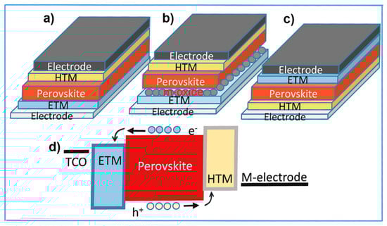
2.1. Device Configurations and Operation

Halide PSCs are typically designed with two main architectures: the conventional n-i-p heterojunction and inverted p-i-n heterojunction structures [49][50] (Figure 1a,c). The n-i-p structured PSCs consist of either mesoporous or planar absorber layer. The former is referred to as mesoporous (n-i-p) PSCs and the latter is referred to as planar (n-i-p) PSCs as shown in Figure 1a,b. While conventional n-i-p PSCs demonstrated higher efficiency to date than p-i-n structured devices, the latter are more exciting for the photovoltaic community due to their ease of fabrication, small hysteresis, and compatibility with tin-based perovskite cells, tandem cells, and flexible PSCs. In a complete device, the perovskite photo-absorber layer is sandwiched between n-type and p-type layers, which serve as electron and hole selective contacts and produce a potential gradient in the perovskite active layer that varies linearly due to the band alignment at thermodynamic equilibrium. Under illumination, the incident photons are absorbed by perovskite active layer, exciting the electron from the valence band (VB) to the conduction band (CB). Subsequently, under a short-circuit condition, a built-in electric field separates the photoexcited electron-hole pairs into free electrons and holes, driving them towards the selective contacts for efficient charge collection [49] as shown in the Figure 1d. It is crucial that the absorber layer has a long carrier lifetime and high carrier mobility to ensure that the photoexcited charge carriers are successfully transported to the respective interfaces. Perfect energy alignment of CB and VB of the perovskite with the CB of the electron transport layer (ETL) and VB of the HTL, respectively, ensures the injection of carriers from the interfaces into the respective transport layers. Finally, high hole mobility of HTL and high electron mobility of ETL guarantee the efficient and smooth extraction and collection of carriers to produce photocurrent and complete the operation of the PSC.
Figure 1. (a) Conventional planar (n-i-p) device structure. (b) Mesoporous (n-i-p) device structure. (c) Inverted (p-i-n) device structure. (d) Charge transportation process in perovskite solar cell.

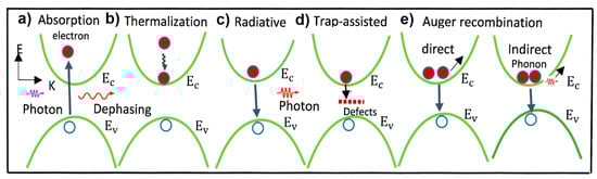
2.2. Charge Carriers’ Recombination Pathways in PSCs

After light absorption and excitation (Figure 2a), the charge carriers with energy greater than the bandgap interact with each other and lose their energy to the conduction band minimum. This process is known as thermalization (Figure 2b). The excited carrier possibly may then undergo one or more primary recombination pathways: radiative recombination (spontaneous band to band) (Figure 2c), trap-assisted Shockley–Read–Hall (SRH) recombination due to low film quality, and interface recombination originating from all the interfaces involved in cells (Figure 2d), and Auger recombination (either direct or indirect) due to electron-phonon interaction (Figure 2e). These defect-induced recombination processes not only reduce the PCE but also trigger the instability of PSCs.
Figure 2. (a) Light absorption and charge excitation process in perovskite absorber. (b) Thermalization process of charge carriers. Specified recombination channels of photo generated carriers including (c) Radiative. (d) Trap-assisted and (e) Auger recombination (both direct and indirect).
The influence of Auger recombination in the PSCs depends on the carrier concentration of the absorbing layer. In the perovskite absorbing layers with a high carrier concentration (>1017 cm−3), the contribution from Auger recombination is quite distinctive among the non-radiative recombination losses [51]. However, defect-assisted recombination, the primary source of non-radiative recombination, mainly depends on the defect density and their energy depth [52][53][54][55]. Equation (1) represents the density of photogenerated free-charge carriers (n) and their recombination mechanism in a complete PSC [56][57]
n t t = G k 3 n 3 k 2 n 2 k 1 n
In the above equation, k1, k2, k3 are rate constants for the trap-assisted, radiative, and Auger recombination, which can be determined by using pump-probe spectroscopy and photoluminescence (PL) decay, and G is the generation rate of charges. For wide-bandgap perovskites, the rate constant for Auger recombination at 1 Sun is negligible, and Auger recombination has little influence. Therefore, trap-assisted recombination dominates as the main recombination loss. Furthermore, the total effective carrier lifetime (τeff) is frequently used to describe the quality of the crystal, which can be defined as τeff = ΔnUeff (Δn is excess local charge carrier density or concentration, and Ueff is the effective recombination rate). Considering all the non-radiative recombination channels in perovskites, the overall carrier lifetime τeff can be described by Equation (2) [58]:
1 τ eff = 1 τ bulk + 1 τ surf + 1 τ Aug + 1 τ SRH +
Equation (2) indicates that the overall carrier lifetime is closely related to all the non-radiative recombination pathways (surface, bulk, interfaces, and the Auger recombination) in the PSCs [59][60]. Thus, suppressing the non-radiative recombination (caused by deep and shallow defect states in the active layer and the interfaces) increases carrier lifetime, leading to improving the device’s overall performance.

2.3. Defect-Induced Trap States and Their Origin

Consider the ideal crystal structure of perovskites, where each ion is located on its equilibrium site. However, in reality, polycrystalline perovskite thin films are fabricated using a low-cost solution process, resulting in various structural defects and unintentional impurities during the post-treatment [61]. These structural defects can be classified as deep-level defects or shallow-level defects, depending on their thermal activation energy. Defects with a thermal activation energy higher than KBT where KB and T represent Boltzmann constant and absolute temperature, respectively, are considered deep-level defects and are suspected to be the main cause of non-radiative recombination in PSCs. The lattice imperfections other than the short-range point defects are one-dimensional (1D) dislocations, 2D-grain boundary defects, 3D precipitates, and the mobile species [62].
The majority of point defects in perovskite crystals, including Ii, MAPb, VMA, VPb, MAi, PbMA, VI, and MAI, have shallow-level defects due to their low formation energies. These defects occupy a higher proportion of overall defect density in perovskite crystals than the deep-level defects. Huang et al. reported that the defects in the perovskites are more likely to be located within bands or the energy levels near the band edges due to the antibonding coupling in the valence band between the p orbital of iodine and a lone pair in s orbital of Pb [63].
Although shallow-level defects are considered benign types of defects due to their much lower charge recombination rate and their little influence on the photovoltaic performance of freshly prepared devices, they possess mobile charge species that can migrate under illumination, heat, and the built-in electric field, leading to unintentional doping effects by accumulating at interfaces [64]. Light-induced ionic redistribution or the migration of defects such as interstitials, antisites, or vacancies can also cause local band bending and impede charge transportation [65], leading to anomalous hysteresis in J-V curve [66][67], degradation of perovskites or metal electrodes [68][69][70][71], and the phase segregation [72][73][74][75]

2.4. Impact of Defect-Induced Non-Radiative Recombination on Device Parameters

The presence of trap states in perovskite thin films and at adjacent interfaces of PSCs, can severely affect their photovoltaic parameters, such as VOC, short-circuit current (JSC), and FF, thereby limiting PCE and stability. Under the bias-illumination, incident light excites electrons from the valence band into the conduction band, splitting the Fermi level (EF) into quasi-Fermi levels of electrons (EFn) and holes (EFp). The steady-state charge density, which is determined by the balance between charge generation and recombination rates, controls the quasi-Fermi level splitting (QFLS = EFn − EFp) [76]. In an ideal case with no recombination in the bulk, at the surface, grain boundaries, and interfaces, the EF of its corresponding carrier would remain constant at the quasi-Fermi level without any drop, and there would be no energy loss. In that case, the output power of the device would be equal to the QFLS [77].
However, when non-radiative recombination creates a pathway for the recombination of excess free charge carriers, it reduces the steady-state charge density and QFLS and, ultimately decreases the VOC of PSCs. Hence, non-radiative recombination is the fundamental source of the open-circuit losses [78]. The relationship between VOC, radiative and non-radiative recombination losses can be described by the external photoluminescence quantum efficiency (ηext) [79][80]:
V OC = V OC , rad + KT q ln η ext
where VOC,rad is the radiative limit of the open-circuit voltage when non-radiative recombination is fully suppressed. Therefore, the deficit in VOC due to nonreductive recombination can be expressed as [81][82]:
V OC , non , rad = V OC , rad V OC = KT q ln PLQY
or   V OC , non , rad = KT q ln EQE EL
Thus, the voltage loss due to non-radiative recombination can be quantified by measuring the photoluminescence quantum yield (PLQY) or electroluminescence quantum efficiency (EQEEL). Improvement in PLQY and EQEEL in passivated PSCs leads to an increase in VOC and a decrease in non-radioactive recombination losses, thereby improving PCE. It has been reported that a 1% improvement in PLQY of PSCs can result in a 0.12 V increase in VOC.

2.5. Defect Induced Hysteresis Behavior and Intrinsic Instability

The hysteretic behavior in the J-V characteristic of PSCs presents a challenge to accurately characterize their photovoltaic performance. Although the exact reasons for this behavior are still under debate, many studies suggest that charge defects and ions migration [83][84] are responsible for the anomalous hysteresis observed in the J-V characteristics of different scanning directions [85][86]. Despite achieving impressive PCE values, most PSCs still suffer from hysteresis [87] and instability [88], which are associated with varying amounts of active charge defect states in the perovskite thin films and device interfaces [83][84]. Ion migration induces intrinsic defects and affects the electric field distribution at interfaces. By using the time-resolved Kelvin probe force microscopy (tr-KPFM) technique, Stefan et al. demonstrated that the hysteresis in PSCs is caused by the localized positive ionic space charge at the ETL surface and negative ionic space charge across the perovskite layer. These charges form an opposite charge layer at the perovskite/ETL interface upon illuminating or applying external voltage. Thus, they attributed the hysteresis to the formation and release of ionic interface charge caused by the variation in illumination or electric field [86]. Their results also confirm that the ion migration toward the interface region impedes the smooth charge extraction and transportation. However, the interplay between ion migration and interfacial defects still requires further exploration.
Several approaches have been proposed to suppress hysteresis in PSCs. One of the most effective methods is the use of additives for the interface, GBs, and ionic defects passivation. FA-based and mixed cationic perovskites have also been found to demonstrate less hysteresis than MA-based PSCs. Another promising technique is the fabrication of 2D/3D graded junctions, which has been shown to reduce hysteresis in mixed-dimensional PSCs. Additionally, an appropriately high scanning rate and improving the crystallinity of the perovskite layer have been found to suppress hysteresis in the PSCs. However, it should be noted that sometimes, scanning direction and rate do not influence the hysteresis. 

3. Estimation of Defect-Induced Recombination Losses and Techniques for Calculating Defect Density

3.1. Calculating the Bandgap

Accurately estimating the bandgap of semiconductor materials is crucial for precise calculations of the VOC deficit caused by trap-assisted recombination occurring in bulk or device interfaces. However, the presence of a substantial number of defects and variation in perovskite film thickness can make it challenging to estimate the bandgap accurately, leading to underestimation or overestimation of recombination losses in the form of VOC deficit in PSCs. Various techniques, such as Kubelka–Munk processes, Tauc plots, and the onset of electroluminescence quantum efficiency (EQE) spectra are used to calculate the bandgap of perovskite thin-film material [89]. The Kubelka–Munk technique calculates the bandgap by measuring the reflection of incident light, while the Tauc plots method utilizes the absorption of incident light in a wide spectral range to determine the bandgap. However, the accuracy in the calculated bandgap for thicker perovskite film is less reliable due to sub-band absorption, resulting in an underestimation of its value. The observed redshift of the onset of EQE spectra is also due to the absorption by electrically active sub-bands.

3.2. Photoluminescence Quantum Efficiency

High photoluminescence quantum efficiency values approaching unity indicate suppression in non-radiative recombination, which is desirable to achieve PCEs close to the theoretically calculated values for single-junction PSCs. If the PLQE value reaches unity, it can be inferred that all non-radiative recombination pathways have been eliminated, and charges are recombining through the emission of photons. When measuring PLQE, incident photons with excitation intensity equivalent to 1 Sun excite carriers to all accessible states, ignoring any imbalance in carrier transport. The relationship between output VOC and the photoluminescence quantum yield (PLQY) is given as [79][90]: 𝑉OC=𝑉OC,rad+KTqln(PLQE). At 1 Sun and excitation density of 1015 cm−3, an increase in PLQY from 1% to unity results in 0.12 V increase in VOC. The obtained PLQY spectra depend on film quality, energy levels matching ETL or HTL with the perovskite layer, and the interfacial recombination channels, as well as other optical losses such as photon escape and parasitic absorption. As PSC is composed of a complex, layered structure, recombination losses in the intrinsic perovskite layer and at the interfaces can be quantified separately. 

3.3. External Radiative Efficiency

Estimation of VOC deficit induced by trap-assisted recombination is often performed using the external radiative efficiency (ERE) under a forward bias with an external voltage source. ERE is typically measured when the injected current under bias is equal to the illumination current. The value of ERE indicates the extent of losses due to non-radiative recombination. A high ERE value indicates low non-radiative recombination losses, suggesting that sufficiently large injected current emits the photons by radiative recombination of carriers [91]. However, the ERE of a complete PSC is generally lower than the PLQY of a perovskite active layer measured alone or in a complete device due to the inequalities in the spatial distribution of the quasi-Fermi levels. The value of ERE can only be compared with the PLQY if the distribution of QFLS remains flat in both measurements.

3.4. Photoluminescence Imaging

The defect states responsible for non-radiative recombination in perovskite absorbers are distributed randomly throughout the bulk, surface, and interfaces. However, the regions near the surface of perovskite film are believed to have a high concentration of trap states. Hyperspectral absolute photoluminescence imaging is a commonly used technique to identify the origin and spatial distribution of defect states in complete PSCs and effectively quantify the trap-assisted recombination losses caused by the defect states at bulk, bottom, and top interfaces.
By using this technique, Stolterfoht et al. [92] showed that the non-radiative recombination losses in the active area are sufficiently non-uniform, and their corresponding losses result in decreasing the QFLS. The interfacial recombination after the incorporation of each charge transport layer individually with perovskite layer (such as poly[bis(4-phenyl)(2,4,6-trimethylphenyl)amine] (PTAA) as HTL and fullerence (C60) as ETL) results in an 80 meV drop in the QFLS at each interface. It is important to note that the loss in VOC due to non-radiative recombination induced by each layer does not simply add up in complete perovskite device operation. Rather, the overall VOC deficit is attributed to the increase in the trap-assisted recombination current, which has a logarithmic relation with VOC.

3.5. Thermal Admittance Spectroscopy (TAS)

Understanding defects and the depths of their energy levels is essential for reducing non-radiative recombination losses in PSCs. TAS is used to obtain detailed information on the trap density of states (tDOS) in a complete PSC. Charged defects in the photoactive layer act as small, localized capacitors, and the trapping-detrapping of carriers in defects is related to the charge-discharge process in the capacitor. By tracing variations in junction capacitance with the frequency of applied alternating current (A.C.) voltage, the features of defects can be deduced. In its working process, first the charged defect states are thermally activated, then they release their charge within the A.C. period and capably foster the admittance signal. The discharging of defects depends on both the depth of the defect energy level and the temperature, which can be reflected by the junction capacitance at varying modulated A.C. frequency. The energy Eω of the defect energy state at a frequency (ω) could be assessed as [61][93]:
E ω = E d E v
In the above equation, Ed and Ev represent the depth of defects energy level and the valance band maximum, respectively. The defect density (Nt) derived from angular frequency-dependent capacitance is given by Equation (7):
N t E w = V bi eW dC dw ω K B T
In Equation (7), ω stands for angular frequency, and C denotes the capacitance. Vbi is a built-in potential and is derived from the capacitance-voltage (C-V) curve. W represents the depletion width, which is taken from Mott-Schottky analysis and expressed as [61][94]:
W = ε 0 ε r A C
In Equation (8), A and εr represent the contact area and relative dielectric constant. Measurements using TAS reveal a larger density of defect states (∼1018 cm−3) in a complete PSC compared to the density of defects in a sole perovskite film in isolated form. The defects induced tDOS having different energy depths usually be categorized into three bands: band 1 lies in an energy interval of 0.35–0.40 eV, band 2 lies between 0.40–0.50 eV, and band 3 lies above 0.50 eV. Some useful approaches for reducing the tDOS include coating a layer of phenyl-C61-butyric acid methyl ester (PC61BM) on the surface of the perovskite active layer, which can effectively decrease the tDOS of band 2 and band 3 almost two orders of magnitude, and surface passivation, which can substantially reduce the deep-level defect states. 

3.6. Steady-State PL Emission

In addition to electrical properties, defects can strongly affect the optical properties of perovskite semiconductors. Therefore, steady-state PL emission has been widely used to estimate the defect density in perovskite films for photovoltaic applications [61][95]. Initially, the perovskite film is photoexcited with pump fluence. After photoexcitation, either the excited charges in perovskite film emits photon through the band-to-band transition, or they become trapped in defect states, resulting in negligible or no emission. If all the defect traps are filled with the photogenerated charges in perovskite thin film, this is indicated by a turning point at low pump fluence, also known as a trap filling turning point. The trap filling turning point at low pump fluence is called a threshold trap pump fluence (𝑃𝑡𝑟𝑎𝑝𝑡) which can be determined by the intersection of the pump fluence axis and linearly extrapolated PL intensity. The total defect density ntrap can be assessed by the following equation [61][95][96]:
n t r a p = P t h t r a p × α E
The term α in Equation (9) stands for the absorption coefficient, whereas E represents the energy of a single photon at the laser pulse wavelength. A higher accuracy in calculating the total defect density can be achieved by using an increased pump fluence for PL emission.

3.7. Space Charge Limited Current (SCLC)

The SCLC technique is another widely used characterization tool for quantifying defect density and carrier mobility and understanding defect-induced trap mechanisms inside the PSCs [97][98][99][100]. In this technique, an adequately large electric field is applied to an electron- or hole-only device via Ohmic contacts and a portion of the ejected electrons/holes is trapped by the defects in perovskite, reducing the density of free charges and limiting the current by the space-charge effect. The dark J-V curves obtained from this technique exhibit three regions: the Ohmic or the linear region, trap-filling limit (TFL) region, and the SCLC region, which is trap-free. The linear region represents the Ohmic response, where current density and electric field intensity have a linear relation (IV). The trap-filling region shows a rapid increase in the current with increasing the electric field (IVn, n > 3), where defect states are continuously filled until all the defects are filled as bias increases. Subsequently, the SCLC trap-free region (IV2) occurs. The trap density (nt) can be calculated using the following equation:
n t = 2 ε ε o V TFL qL 2
where, ε represents the dielectric constants for the photoactive layer, ε0 represents the vacuum permittivity, L represents the thickness of the perovskite active layer, and q represents the elementary charge. VTFL is the bias voltage required to occur the TFL region, which can be obtained from the dark J-V by fitting. The dielectric constant of the photoactive layer (perovskite) can be calculated from Equation (11):
ε = C g L ε 0 A
where, Cg denotes the geometrical capacitance of the active layer, ε0 = 8.85 × 10⁻¹⁴ F·cm−1 is permittivity of free space, and A represents the active area of the device [101]. Note that this technique only calculates the single type of defects for electron traps or hole traps at a time.

3.8. Deep-Level Transient Spectroscopy (DLTS)

DLTS is a technique that is used to detect deep-level traps that are difficult to detect by other characterization techniques [61][102][103][104]. It is significant because of its sensitivity, ease of operation, and its ability to set a window for emission rates [103]. The DLTS utilizes the variation in defect emission rates with temperature to define the energy difference between one of the band edges and the defect states in the forbidden gap and to estimate the capture cross-section of the defects [102]. The capacitance transients are explored using the DLTS technique by evaluating the variations in capacitance with variation in temperature (from the temperature of liquid nitrogen to the room temperature or above). The defect states are filled up by the charges generated under an initial low-temperature bias pulse. In this case, the emitting rate of a trap state is much lower than its capturing rate and the former can be neglected [61]

4. Novel Defect Management Strategies to Mitigate Defect-Induced Losses and Instability Issues

4.1. Bulk or the Deep Level Defects Passivation Techniques

4.1.1. Compositional Engineering

Compositional engineering is one of the most successful techniques for regulating the optoelectronic properties of perovskite thin films, including light absorption, carrier mobility, defect density, and carrier concentration. This method allows for the modification of the perovskite film morphology and crystallinity through cationic or ionic doping [105][106].
Hence, the optoelectronic properties of perovskite are directly or indirectly influenced by A- and B-site cations and X-site anions [106]. Engineering at the cationic or anionic sites through mixed anions and cations or suitable substitution in standard perovskite structure can suppress non-radiative recombination and improve PCE and stability. 
X-site engineering: Early PSCs made with MAPbI3 exhibited low PCE due to poor crystallinity and morphology of the perovskite film. However, Jeon et al. were able to achieve a PCE of 16.2% by substituting Br for I in the perovskite composition and using the anti-solvent dipping technique to suppress defects during crystal growth [107]. Noh et al. also achieved a PCE of 12.3% by using a mixed halide MAPb(I1−xBrx)3 composition to tune the bandgap and improve the device stability [108]. The mixed composition MAPb(I1−xBrx)3 can tune the bandgap in the range from 1.53 eV to 2.97 eV and provides high-efficiency colored PSCs [108][109].
Both A and X sites engineering: The large bandgap of MAPbI3 (∼1.55 eV), which is greater than the Shockley–Queisser optimum of ∼1.4 eV for single-junction solar cells, means that it cannot absorb the full solar spectrum. Doping with the larger formamidinium (FA) cation can reduce the bandgap to around 1.48 eV, improving optical and electrical properties and leading to higher JSC and PCE of PSCs. Additionally, reports suggest that the MA cation rotation can passivate deep-level defects such as iodide and lead vacancies, making A-site cation more influential in the traps, charge transport, and light absorption of perovskite devices. FA is more thermally stable than MA cation, making it a suitable doping candidate for device stability.
Stabilizing the photoactive α-phase of FAPbI3: Compared to MAPbI3-based PSCs, FAPbI3-based PSCs have a reduced bandgap of 1.48 eV due to the slightly larger size of FA cation, which enhances light absorption and potentially leads to higher JSC and PCE closer to the SQ limit. However, their stability is comparatively lower than that of MAPbI3-based perovskite due to their tolerance factor, which falls close to the upper boundary of the Goldschmidt chart. Moreover, the structural instability of FAPbI3 at room temperature remains a challenge as it can crystallize to an undesired, photo-inactive hexagonal δ-phase with a wide bandgap [110]. The room-temperature stable hexagonal phase has a high tolerance factor and activation energy, which can be reduced by using mixed cations, anions, or additives to promote the formation of the desired stable black perovskite phase. However, even the trigonal photoactive α-phase or a black perovskite phase is also sensitive to humidity and high α-phase transition temperature, which makes this composition more challenging.

4.1.2. Bulk Passivation with Alkali Metal Cations

Defects such as iodine interstitials (Ii) in the perovskite absorber are generated during the growth process, resulting in an accelerated non-radiative recombination of photo-generated electron-hole pairs and decreased PCE of the perovskite devices. These iodine interstitials can readily migrate due to their low activation energy (0.29 eV) [111], causing undesirable current-voltage hysteresis and device instability [111][112]. Both the theoretical and experimental results confirm that the introduction of alkali metal halides (potassium iodide (KI), cesium iodide (CsI), lithium iodide (LiI), cesium chloride (CsCl), sodium fluoride (NaF, etc.) into the perovskites solution effectively suppresses bulk defects as well as defects along surface and GBs, inhibiting ions migration and anomalous hysteresis, and thereby improving carrier lifetime and the overall device performance.
Abdi-Jalebi et al. demonstrated that the addition of an optimized amount of potassium iodide (KI) solution in triple cations perovskite (Cs0.06FA0.79MA0.15)Pb(I0.85Br0.15)3 solution successfully suppresses the non-radiative recombination by passivating halide vacancies and eliminates hysteresis by suppressing photoinduced ion migration in perovskite films [72]. The improvement in luminescence yields was attributed to the decrease in bandgap and surface and GBs defects passivation by the formed layer of KI at the surface of perovskite absorber layer. The origin of hysteresis in PSCs, as confirmed by several theoretical studies, is not the migration of iodine vacancies but the formation of Iodine Frenkel (I Frenkel) defects [41]

4.1.3. Bulk Passivation with Divalent Metal Cations

Divalent metal cations such as calcium cation (Ca2+), strontium cation (Sr2+), europium cation (Eu2+) etc. are frequently used to stabilize the perovskite α-phase and improving device performance, particularly in the inorganic CsPbI2Br PSCs [113][114][115]. Han et al. [113] reported the calcium chloride (CaCl2) in CsPbI2Br for n-type doping in perovskite lattice. The Ca2+ ions passivated the GBs defects by combining with Cl ions instead of incorporating in the lattice, increasing the Fermi level splitting, and delivering a very high VOC of 1.32 V. The defect density decreased from 9.10 × 1015 cm−3 to 3.03 × 1015 cm−3 in passivated devices. Wang et al. reported the addition of europium ion pair of Eu3+-Eu2+ acting as a “redox shuttle” to oxidize deep-level Pb cluster (Pb0) defect and reduce I0 defect in a cyclical redox transition process in PSCs [115]. The redox shuttle transfers electrons to I0 defects from Pb0, where Pb0 is oxidized to Pb2+ by the Eu3+ cation and the formed Eu2+ concurrently reduces I0 to I. The passivated devices demonstrated a high PCE of 21.52% and improved long-term stability by retaining 90% of the initial efficiency after 8000 h. Similarly, the Sr2+ has been reported for partial substitution of toxic lead with less toxic doped strontium metal and its strong defects passivation in inorganic PSCs. The doped Sr enriched the CsPbI2Br surface and increased the FF and VOC by passivating the defects [114].

4.1.4. Bulk Passivation with Transition Metal Halides

Transition element halides such as NiCl2, NbF5, manganese ion (Mn2+), and cadmium iodide (CdI2), have been employed to suppress the formation of deep-level defects Pb0 and undercoordinated I ions and I-rich antisites), thereby improving the performance and structural/phase stability of PSCs [116][117][118]. These transition metals, having filling d-orbits, can form strong bonds with various ligands to create stable coordination and effectively suppress migration.

4.1.5. Bulk Passivation with Halide Anions

The halogen ions such as Cl, F, I are commonly used as additives in perovskite solutions to control the perovskite crystal growth process, suppress defects, and improve the morphology of the perovskite absorber layer [119]. These ions can be introduced by adding compounds such as ammonium chloride (NH4Cl), lead chloride (PbCl2), CsCl, CsI, MACl, lithium fluoride (LiF), formamidine chloride (FACl), NbF5, trimethylammonium chloride (TACl), and N,1-diiodoformamidine (DIFA). Among them, Cl is the most extensively studied ion, as it can improve the morphology of perovskite film by slowing down crystallization and enlarging grain size. Even though Cl can quickly escape during thermal annealing, the residue can improve device performance by passivating defects at the GBs [120][121].

4.2. Grain Boundaries Passivation

4.2.1. GBs Passivation with Alkyl Salts

The performance of p-i-n structure perovskite is generally inferior to regular n-i-p PSCs. However, Zheng et al. [122] reported the high-efficiency inverted PSCs by using trace amount (<0.3 mol.%) of long-chain alkylamine ligands (AALs) including phenethylamine (PEA), n-butylamine (BA), oleylamine (OA), and octylamine (OAm) directly in the mixed cation perovskite precursors in one-step coating method. The long alkyl chain increases moisture stability while the amine group passivates the A-side vacancy defects. Octylamine was found to have a stronger passivation effect than other alkylamine ligands, with a large improvement in carrier lifetime from 114 ns in pristine to 1049 ns in OAm passivated perovskite films. Furthermore, the passivated devices demonstrated a lower trap density of 4.4 × 10²² m−3 eV−1 at shallower energy (0.32 eV) than 1 × 10²³ m−3 eV−1 at 0.35 eV in pristine film at room temperature (300 K). The improved film quality and optoelectronic properties resulting from optimized passivation of OAm led to a significant improvement in VOC from 1.06 V to 1.17 V and PCE from 20.5% to 23.0%.

4.2.2. GBs Passivation with Zwitterions

Zwitterions are widely reported passivation agents which can coordinate with both positively charged undercoordinated Pb2+ cationic defects and negatively charged Pb-I antisite defects, because they have both electron donor and acceptor groups. Thus, they are also known as bifunctional molecules [123]. In 2017, Zheng et al. developed and reported three zwitterion molecules (L-α-phosphatidylcholine, choline chloride, and choline iodide) for passivating cationic and anionic defects in FA0.85MA0.15Pb(I0.85Br0.15)3-based PSCs [124]. All three passivators showed a remarkable improvement in VOC and increased carrier lifetimes, with choline chloride delivering the best results, demonstrating a big improvement in VOC from 1.03 V to 1.14 V with only 0.39 V deficit and PCE from 19.2% to 21.0%. The devices stored in ambient conditions showed no change in PCE after 800 h.

4.2.3. GBs Passivation by Lewis Base Molecules

A diverse range of Lew7is base molecules, including molecules, polymers, and π-conjugated materials containing electron donor sulfur (S), nitrogen (N), and oxygen (O) atoms, are employed for passivating defects in PSCs [125][126][127][128]. These molecules can effectively suppress the undercoordinated Pb2+ or Pb cluster defects at GBs or the surface of perovskite thin films by forming Lewis adducts with defective trap-states when an optimized small quantity is added in the precursor solution.
Sanith et al. [129] initiated defects passivation with Lewis bases using pyridine and thiophene as organic Lewis bases in their study. They demonstrated that the undercoordinated Pb2+ defects are passivated by the lone pair of electrons on the S atom of thiophene and the N atom of pyridine by forming coordination bonds.
Small molecules containing conjugated carboxyl (C = O) groups have also been proven to improve stability and passivate GBs defects in PSCs with their O donor carboxyl groups. For example, Wang et al. [130] introduced 1,3,7-trimethylxanthine, also known as caffeine, in MAPbI3 precursor solution to improve PCE and thermal stability of the devices. The additive has two conjugated carboxyls (C = O) groups that passivate positively charged defects by strongly interacting with Pb2+ and suppress ionic migration. 

4.2.4. GBs Passivation with Lewis Acids

Lewis acids are also often used as additives in precursor solution or incorporated in antisolvent for in-situ passivation during the deposition and crystallization of perovskite films. By adding a small amount of electron acceptor Lewis acids, electron-rich defects such as Pb-I antisite or the undercoordinated iodide (I) ions with extraneous electron pairs can be passivated. For example, fullerene (C60) and its derivatives (indene-C60 bis-adduct (ICBA), [6,6]-phenyl-C61-butyric acid methyl ester (PCBM) etc.) have shown good passivation effects due to the strong electron-accepting ability of their fullerene spherical structure. In a study by Wu et al. [131] the addition of PCBM in PbI2 precursor solution was shown to form pinhole-free perovskite thin films by a two-step deposition method. The added PCBM passivated the negatively charged vacancy defects at GBs. Although PCBM does not exist in the lattice. It was distributed along the GBs due to its too large size, as confirmed by electron energy loss spectroscopy (EELS) mapping. The improved quality and optoelectronic properties of perovskite films led to a high FF of 0.82 and a high PCE of 16%.

4.2.5. GBs Passivation with Polymers

The long-chain polymers composed of different donor functional groups are commonly used in PSCs to improve their stability and performance by passivating defects predominantly at the GBs [43][126][132]. Due to their large molecular size, they can distribute along the GBs rather than being incorporated in the perovskite lattice and prevent the moisture penetration through GBs.

4.2.6. GBs Passivation by Multifunctional Agents

The use of multifunctional passivation molecules in PSCs has become increasingly popular due to their ability to improve both device stability and performance by simultaneously passivating multiple trap-assisted recombination pathways [133]. For example, Cai et al. [134] reported 2,2-difluoropropanediamide (DFPDA), a multifunctional molecule, into the FA0.85MA0.15PbI3 precursor solution. DFPDA contains fluorine, carbonyl, and amino groups, which can passivate undercoordinated Pb2+ defects by making a chemical bond with carbonyl group, suppress ion migration by immobilizing the iodide by amino group, and increase the moisture stability by making a barrier on the perovskite film with fluorine group.

4.2.7. GBs Passivation with Ionic liquids (ILs)

Many research groups have highlighted the multifunctional role of ionic liquids (ILs) in the development of PSCs. The structure of ILs contains large cationic functional groups and organic or inorganic anions, and the strong electrostatic force between ions enables them to minimize both negative (halide vacancies) and positive defects (Pb2+), thereby improving device performance, structural, thermal, and humidity stability of the perovskite devices.

4.2.8. GBs Passivation with Quantum Dots (QDs)

Numerous reports have confirmed that effectiveness of using quantum dots (QDs) as agents for passivating surface and GBs defects passivation agents in PSCs, thereby improving and stabilizing their performance [135][136]. Carbon QDs, possessing amino, hydroxyl and the carbonyl functional groups, can passivate electronic defects at the GBs, suppressing non-radiative recombination [137][138]. For instance, Huang et al. reported the passivation of undercoordinated Pb2+ trap states at GBs by adding carbon QDs with carbonyl and hydroxyl passivation groups. The passivated perovskite films displayed extended carrier lifetime, and higher PL intensity than control perovskite thin films and the corresponding passivated devices demonstrated a higher PCE of 18.24% than that of control MAPbI3 devices (15.67%).

4.2.9. GBs Passivation with Oxides

Oxides of metals and nonmetals are found to be effective in stabilizing the performance of PSCs by passivating defects. The oxides of Group IV B and II A elements, such as silicon dioxide (SiO2), aluminium oxide (Al2O3), sodium oxide (Na2O), lithium oxide (Li2O), and boron oxide (B2O3), are especially useful due to their high thermal stability. These oxides have been reported to suppress GBs and interfacial defects, thereby improving the stability and performance of the device.

4.3. Surface Defects Passivation by Post-Treatments

4.3.1. Post-Treatment with Lewis Acids

Lewis acids can effectively passivate not only GB defects by their addition in precursor solution or in antisolvents but also electron-rich defects (undercoordinated I) on the surface through post-treatment of crystallized perovskite films. Negative defects act as Lewis bases and donate their electrons to surface passivating Lewis acid, thus forming a Lewis adduct to passivate the surface defects and improve the overall performance of the perovskite device. For instance, Huang et al. [93] coated a very thin layer of PCBM on the top surface of perovskite and confirmed through thermal admittance spectroscopy results that the fullerene derivative had passivated the defects on the surface and at the GBs. The surface treatment eliminated the photocurrent hysteresis and doubled the PCE by suppressing trap density up to two orders of magnitude.

4.3.2. Post-Treatment with Lewis Base Molecules and Functional Groups

Lewis base small molecules with N, S or O donors, long-chain polymers with 𝜋
-conjugated functional groups such as carbonyl (–C =
O) and cyanide, having delocalized electrons, and molecules with benzene rings and amino donor groups are commonly used to passivate undercoordinated Pb2+ or Pb cluster produced by halogen vacancies [128]. Post-treatments of perovskite active layers with such long-chain polymers improve both efficiency and the moisture stability of the device [139].
In perovskite solar cells, surface defects passivation with Lewis bases was first initiated by Noel et al. [129]. They employed thiophene with S donors and pyridine with N donors for surface treatment, which passivated the under-coordinate Pb2+ defects by lone pair of electrons on the S atom of thiophene and the N atom of pyridine by forming coordination bonds. Between these two additives, the pyridine demonstrated a better passivation effect than thiophene due to the higher electronegativity of the N atom than the S atom of thiophene. Therefore, the strong electron-donating ability enables pyridine to coordinate more strongly with Pb2+.

4.3.3. Post-Treatment with Hydrophobic Molecules

The long-term stability of the perovskite device is greatly affected by the intrusion of water and oxygen in the atmosphere. Hydrophobic materials are generally non-polar and do not absorb water. They can passivate charge trapping centers on the surface while enhancing the hydrophobicity of the perovskite layer with their specific passivation groups (i.e., carbonyl, fluorine). Therefore, surface treatment with the hydrophobic materials has become a promising approach to simultaneously improve the stability and the PCE of PSCs [140][141][142].

4.3.4. Post-Treatment with Hydrophilic Molecules

In contrast to the use of hydrophobic passivation agents, Park et al. [143] reported a novel bifunctional approach of spin-coating hydrophilic materials, 2-aminoethanol hydroiodide (2AEI), and 4-amino-1-butanol hydroiodide (4ABI), onto the surface of the absorber layer to simultaneously enhance stability and device performance. These hydrophilic materials form strong chemical bonds with trap states such as iodide centers and undercoordinated Pb2+ ions, suppressing the bulk and surface defects. In addition, they improve the crystallinity of the absorber layer. The excellent passivation effects of 4ABI and 2AEI are reflected by the substantial enhancement in PL, extended carrier lifetime, and reduction in defect density. The estimated defect density reduction from 1.2 × 1016 cm−3 (control) to 1.0× 1016 cm−3 (4ABI and 2AEI) and significant improvement in carrier lifetime (from 245 to 611 ns with 4ABI) demonstrate the suppression in non-radiative recombination of charge carriers.

4.3.5. Post-Treatment with Alkyl Chain Organic Cations

Another approach to manage both anionic and cationic defects on perovskite surfaces and GBs is to use alkyl chain organic cations such as alkylammonium halides as a capping layer on the top of perovskite surface through a post-treatment method. This method passivates ionic defects at the surface and GBs through electrostatic binding and can potentially form a 2D layered perovskite on the top surface of the absorber layer to suppress interfacial recombination and improve stability against moisture. However, the formation of 2D layered perovskite may affect the charge transfer process and lower the performance [144][145]. Organic cations with long alkyl chains such as NH3I(CH2)8NH3I (C8), octylammonium (OA+), and tertbutylammonium (tBA), are unable to be doped into the perovskite lattice due to their large size and high formation energy, but they can form layered perovskites to suppress defects on the surface and GBs of absorber layer [146][147].

4.3.6. Post-Treatment with Wide Band Gap Materials as Capping Layer

The use of wide band gap materials as post-treatment capping layers is another approach for surface passivation of perovskite. Typically, anions such as phosphate, sulfate, sulfur, or inorganic oxides can interact with surface dangling bonds or positive lead ions, contributing to the suppressing of non-radiative recombination and improvement in stability.

4.4. Interfacial Defect Passivation

4.4.1. Dimensionality Engineering

The mixed-dimensional perovskites have become an effective approach to improve device performance and stability for their commercialization [148]. The use of 2D/3D bilayer structure in PSCs is proposed as an efficient approach to eliminate recombination centers at interfaces, surface or GBs, and suppress electron density at HTL and perovskite layer due to electron repelling nature of wide bandgap 2D materials, thereby leading to improving the device stability and PCE [48][149]. To form a 2D/3D heterojunction, a very thin layer of aliphatic or aromatic alkyl ammonium cations is coated on the top surface of the 3D bulk perovskite layer [32], or alkylammonium salt is introduced into 3D perovskite precursor solution by in situ formations.
In 2016, Docampo et al. [150] developed a solution process using MAI and phenylethylammonium iodide (PEAI) in isopropyl alcohol (IPA) to fabricate layered 2D perovskite on the top surface of 3D MAPbI3 perovskite. The top thin layer of 2D perovskite (PEA)2(MA)4Pb5I16 serves as a moisture barrier and enables the selective charge extraction owing to the well-aligned energy band, leading to suppression of non-radiative recombination at the interface. The underlying active MAPbI3 layer guarantees full white light absorption and carrier generation. Due to the significant passivation effects of 2D layered perovskite, a realistic improvement in PCE from 13.61% in pure MAPbI3 to 16.8% in the mixed (2D/3D) perovskites was achieved. As VOC and FF values of a device are closely related to trap-assisted recombination, the improvement in VOC (from 0.99 to 1.11 V) and FF (from 0.70 to 0.73) indicates the suppression of recombination losses in PSCs with this two-layer configuration.

4.4.2. Interfacial Defects Passivation by Interlayer Engineering

PSCs consist of an absorber layer sandwiched between two charge transporting layers, which transport the photogenerated carriers [151]. The charge extraction and transport ability of these layers are equally important to the charge generation process in the active layer. Therefore, interfaces play a critically important role in the device, especially energy alignment between the absorber and charge transporting layer, which largely influences the device performance and stability. The defect density at all the interface of PSCs is reported to be one to two orders of magnitude higher than that in bulk of the photoactive layer [152].
The energy level mismatch between EFn in the perovskite layer and CB/lowest unoccupied molecular orbital (LUMO) of ETL, or between the EFp in the absorber layer and VB/HOMO of HTL, results in band bending at the interfaces [81]. This band bending reduces the QFLS of the compact device, leading to a decrease in output voltage under illumination. It has been reported that almost all charge transporting layer decrease VOC due to non-radiative interfacial recombination currents induced by them, except for high-efficiency devices that have well aligned energy bands with absorber layer.
Interfacial layer between HTL and perovskite. To realize the full potential of perovskites as photovoltaic material in PSCs, the suppression of carrier recombination at the perovskite/HTL interface is critical. This is because the built-in electric field at HTL/perovskite interface becomes weak due to the intrinsic self-doping characteristic of perovskites, which hinders the adequate transportation of carriers from the absorber to HTL [153]. Currently, the most efficient HTL is spiro-OMeTAD, which is often heavily doped to enhance its conductivity, resulting in increased recombination losses at the HTL/perovskite interface. Decreasing the doping concentration in the spiro-OMeTAD has been reported to suppress interfacial recombination, increase VOC and improve the device performance [154][155].
Interlayers between ETL and perovskite. The electron transporting layer (ETL) plays a critical role in perovskite devices, as it is essential for effective charge extraction and transportation. A well-aligned energy level between the ETL and perovskite layer and defect-free interface crucial for achieving high VOC [156]. This goal can be accomplished by introducing a thin interlayer of suitable material between the two layers. While titanium dioxide (TiO2) is the most efficient and commonly used ETL material, it is susceptible to light-induced instability, particularly under ultraviolet (UV) radiation. Light exposure generates electron-hole pairs in TiO2. The holes in the valence band recombine with available electrons on oxygen adsorption sites, leaving the positive oxygen vacancies or the Ti3+ sites on the surface of TiO2 and the free electrons in the conduction band [157]. Therefore, introducing an ultra-thin layer between ETL (TiO2) and perovskite is an efficient approach to mitigate these issues and suppress carrier traps and interfacial recombination, thereby improving stability and the performance of the devices.

5. Defects Passivation Techniques for Large Area Perovskite Solar Cells and Modules

5.1. Influence of Additives in Large-Area MAPbI3 PSCs and Modules

Li et al. [158] added a small amount of monoammonium zinc porphyrin (ZnP) additive into the perovskite precursor solution for fabricating large-area perovskite films. The ZnP compound can efficiently anchor on the surface and GBs of perovskite film, suppressing the surface and GBs defects. It also prevents the escape of volatile organic cations during thermal annealing and acts as a barrier to moisture invasion. The passivated devices exhibited excellent thermal and moisture stability. Furthermore, the addition of ZnP to the precursor solution reduced the contact angle on the substrate and facilitated full surface coverage in blade coating, resulting in pinhole-free and uniform grain size. Finally, with the remarkable passivating effect of ZnP, large-area (16 cm2) PSCs with improved thermal and moisture stability were successfully fabricated.

5.2. Influence of Additives in Roll-to-Roll Fabrication of PSCs

The optoelectronic properties of photoactive perovskite material can be altered by the mixed cationic and anionic composition, while additives can passivate defects and control the film growth process, thereby leading to improved PCE and thermal and moisture stability of large-area devices. In 2019, Kim et al. demonstrated the use of two additives, PbCl2 (2.5 mg/mL) and MACl (2.5 mg/mL) in MA0.6FA0.38Cs0.02PbI2.975Br0.025 precursor solution, along with a slightly modified PEDOT:PSS, to stabilize photovoltaic performance and improve the stability of the first fully roll-to-roll (R2R) fabricated PSCs [159]. The two additives and the polymer modification in the HTL layer improved all the performance parameters and prolonged stability. The MACl additive improved the quality of film, increased carrier life time and increased the current density of the devices [160]. Similarly, the improvement in VOC and the FF was attributed to the passivation effects of PbCl2. Furthermore, the polymer modification in HTL enables the deposition of perovskite in high humidity environment (approx. 55% RH). Finally, fully R2R slot die coated PSC with a remarkable efficiency of 11.7% was reported, except for top contact [159].

6. Conclusions

Due to the high formation energy of deep-level trap states and low-temperature fabrication of perovskite thin films, substantially reduced nonradioactive recombination sites exist in bulk. However, shallow trap states with low defect densities are easily produced at the surface and GBs of the perovskite layer due to its low-temperature solution fabrication. The existence of shallow trap states at the surface mainly causes non-radiative recombination of photogenerated carriers and results in VOC deficit and reduction in FF of the PSCs. Although the efficiency of single-junction perovskite is approaching theoretically calculated value, state-of-the-art PSCs still exhibit a VOC deficit of 0.32–0.35 V, which suggests the presence of non-radiative recombination channels at the surface, GBs, and interfaces. Photoinduced ion migration and accumulation at interfaces mostly account for the anomalous hysteresis in PSCs. Mixed composition Cs0.05(MA0.17FA0.83)0.95Pb(I0.83Br0.17)3 PSCs exhibit negligible hysteresis compared to MAPbI3 in mesoporous PSCs, making compositional engineering a feasible strategy to suppress bulk defects and improve stability and optoelectronic properties to obtain hysteresis-free devices. Similarly, a mixed perovskite 2D/3D heterojunction is a successful approach for improving stability due to high stability and defect passivation of 2D perovskite at the surface, GBs, and interface. The most stable PSCs, with a stability of over 1 year and an efficiency >

24% has been obtained through this method. However, accurate control of 2D/3D heterojunction formation and understanding the mechanisms involved remain a challenge. Therefore, it is a pressing need to explore the new 2D materials to fine-tune the 2D/3D graded junction. To achieve this, a machine learning tool can be applied, which may provide a complete analysis from materials selection to the device performance.
Interfacial layers have proven to be effective in improving the performance and stability of PSCs by reducing the band bending, ion migration, and accumulation at interfaces. The mismatch between energy levels at the interface causes band bending, leading to a reduced output voltage of PSC under illumination. Interfacial buffer layers minimize this effect, improving the charge extraction and transportation process and resulting in device efficiency up to 23.7% with improved stability. To further enhance the stability and efficiency, exploring new hydrophobic materials with proper energy level alignment and high conductivity is promising.
Chemical additives are commonly used to control perovskite crystal growth, improve thin film morphology and passivate defects, thereby eliminating hysteresis and improving stability and device performance. A variety of passivating additives are available to suppress trap-assisted non-radiative recombination in PSCs, including the alkali metal halides in perovskite solution, which effectively reduce hysteresis and passivate the point defects at the surface and GBs.
Machine learning could be a beneficial tool for designing new passivation agents along with intensive high-throughput experimental investigation. In addition to addressing trap-assisted recombination losses and stability, the scalable fabrication of devices and modules is the third significant challenge. As the coating area increases, the PCE of corresponding devices displays a significant downward shift. Large-area coating processes to produce high-quality crystals pose a challenging task. Chemical additives and physical techniques are usually applied to the large-area fabrication of perovskite films. The additives passivate the trap-assisted recombination of photogenerated charge carriers and facilitate controlling the grain growth process, which leads to improving the quality of perovskite thin films and the performance of the devices.
To further improve the efficiency, stability, and scalability of PSCs, it is crucial to gain a more in-depth comprehension of the origin and nature of non-radiative recombination losses and to judiciously select passivating molecules with the aid of machine learning tools and experimental investigation. Moreover, the combined effect of using the 2D/3D graded heterojunction materials, compositional engineering, and additives to control the crystal growth process may prove more beneficial for improving the stability and PCE of large-area devices.

References

  1. Green, M.; Dunlop, E.; Hohl-Ebinger, J.; Yoshita, M.; Kopidakis, N.; Hao, X. Solar cell efficiency tables (version 57). Prog. Photovolt. Res. Appl. 2021, 29, 3–15.
  2. Dong, Q.; Fang, Y.; Shao, Y.; Mulligan, P.; Qiu, J.; Cao, L.; Huang, J. Electron-hole diffusion lengths > 175 m in solution-grown CH3NH3PbI3 single crystals. Science 2015, 345, 967–970.
  3. Stranks, S.D.; Eperon, G.E.; Grancini, G.; Menelaou, C.; Alcocer, M.J.P.; Leijtens, T.; Herz, L.M.; Petrozza, A.; Snaith, H.J. Electron-Hole Diffusion Lengths Exceeding 1 Micrometer in an Organometal Trihalide Perovskite Absorber. Science 2013, 342, 341–344.
  4. Xing, G.; Mathews, N.; Sun, S.; Lim, S.S.; Lam, Y.M.; Grätzel, M.; Mhaisalkar, S.; Sum, T.C. Long-Range Balanced Electron- and Hole-Transport Lengths in Organic-Inorganic CH3NH3PbI3. Science 2013, 342, 344–347.
  5. Jodlowski, A.; Rodríguez-Padrón, D.; Luque, R.; de Miguel, G. Alternative Perovskites for Photovoltaics. Adv. Energy Mater. 2018, 8, 1703120.
  6. Yang, S.; Fu, W.; Zhang, Z.; Chen, H.; Li, C.-Z. Recent advances in perovskite solar cells: Efficiency, stability and lead-free perovskite. J. Mater. Chem. A 2017, 5, 11462–11482.
  7. Li, Z.; Klein, T.R.; Kim, D.H.; Yang, M.; Berry, J.J.; van Hest, M.F.A.M.; Zhu, K. Scalable fabrication of perovskite solar cells. Nat. Rev. Mater. 2018, 3, 18017.
  8. Guo, F.; Qiu, S.; Hu, J.; Wang, H.; Cai, B.; Li, J.; Yuan, X.; Liu, X.; Forberich, K.; Brabec, C.J.; et al. A Generalized Crystallization Protocol for Scalable Deposition of High-Quality Perovskite Thin Films for Photovoltaic Applications. Adv. Sci. 2019, 6, 1901067.
  9. Yamamoto, K.; Yoshikawa, K.; Uzu, H.; Adachi, D. High-efficiency heterojunction crystalline Si solar cells. Jpn. J. Appl. Phys. 2018, 57, 08RB20.
  10. Wolff, C.M.; Caprioglio, P.; Stolterfoht, M.; Neher, D. Nonradiative Recombination in Perovskite Solar Cells: The Role of Interfaces. Adv. Mater. 2019, 31, 1902762.
  11. Bisquert, J.; Juarez-Perez, E.J. The Causes of Degradation of Perovskite Solar Cells. J. Phys. Chem. Lett. 2019, 10, 5889–5891.
  12. Deretzis, I.; Smecca, E.; Mannino, G.; La Magna, A.; Miyasaka, T.; Alberti, A. Stability and Degradation in Hybrid Perovskites: Is the Glass Half-Empty or Half-Full? J. Phys. Chem. Lett. 2018, 9, 3000–3007.
  13. Smecca, E.; Numata, Y.; Deretzis, I.; Pellegrino, G.; Boninelli, S.; Miyasaka, T.; La Magna, A.; Alberti, A. Stability of solution-processed MAPbI3 and FAPbI3 layers. Phys. Chem. Chem. Phys. 2016, 18, 13413–13422.
  14. Correa-Baena, J.P.; Saliba, M.; Buonassisi, T.; Grätzel, M.; Abate, A.; Tress, W.; Hagfeldt, A. Promises and challenges of perovskite solar cells. Science 2017, 358, 739–744.
  15. Kim, H.S.; Seo, J.Y.; Park, N.G. Material and Device Stability in Perovskite Solar Cells. ChemSusChem 2016, 9, 2528–2540.
  16. Li, X.; Wang, Y.-C.; Zhu, L.; Zhang, W.; Wang, H.-Q.; Fang, J. Improving Efficiency and Reproducibility of Perovskite Solar Cells through Aggregation Control in Polyelectrolytes Hole Transport Layer. ACS Appl. Mater. Interfaces 2017, 9, 31357–31361.
  17. Meng, L.; You, J.; Yang, Y. Addressing the stability issue of perovskite solar cells for commercial applications. Nat. Commun. 2018, 9, 5265.
  18. Odabaşı, Ç.; Yıldırım, R. Assessment of Reproducibility, Hysteresis, and Stability Relations in Perovskite Solar Cells Using Machine Learning. Energy Technol. 2020, 8, 1901449.
  19. Wali, Q.; Iftikhar, F.J.; Khan, M.E.; Ullah, A.; Iqbal, Y.; Jose, R. Advances in stability of perovskite solar cells. Org. Electron. 2020, 78, 105590.
  20. Saliba, M.; Matsui, T.; Seo, J.-Y.; Domanski, K.; Correa-Baena, J.-P.; Nazeeruddin, M.K.; Zakeeruddin, S.M.; Tress, W.; Abate, A.; Hagfeldt, A.; et al. Cesium-containing triple cation perovskite solar cells: Improved stability, reproducibility and high efficiency. Energy Environ. Sci. 2016, 9, 1989–1997.
  21. Wu, B.; Nguyen, H.T.; Ku, Z.; Han, G.; Giovanni, D.; Mathews, N.; Fan, H.J.; Sum, T.C. Discerning the Surface and Bulk Recombination Kinetics of Organic–Inorganic Halide Perovskite Single Crystals. Adv. Energy Mater. 2016, 6, 1600551.
  22. Ball, J.M.; Petrozza, A. Defects in perovskite-halides and their effects in solar cells. Nat. Energy 2016, 1, 16149.
  23. Snaith, H.J.; Abate, A.; Ball, J.M.; Eperon, G.E.; Leijtens, T.; Noel, N.K.; Stranks, S.D.; Wang, J.T.-W.; Wojciechowski, K.; Zhang, W. Anomalous Hysteresis in Perovskite Solar Cells. J. Phys. Chem. Lett. 2014, 5, 1511–1515.
  24. Azpiroz, J.M.; Mosconi, E.; Bisquert, J.; De Angelis, F. Defect migration in methylammonium lead iodide and its role in perovskite solar cell operation. Energy Environ. Sci. 2015, 8, 2118–2127.
  25. Yuan, Y.; Huang, J. Ion Migration in Organometal Trihalide Perovskite and Its Impact on Photovoltaic Efficiency and Stability. Acc. Chem. Res. 2016, 49, 286–293.
  26. Yang, Y.; Peng, H.; Liu, C.; Arain, Z.; Ding, Y.; Ma, S.; Liu, X.; Hayat, T.; Alsaedi, A.; Dai, S. Bi-functional additive engineering for high-performance perovskite solar cells with reduced trap density. J. Mater. Chem. A 2019, 7, 6450–6458.
  27. Li, Y.; Fan, D.; Xu, F.; Shan, C.; Yu, J.; Li, W.; Luo, D.; Sun, Z.; Fan, H.; Zhao, M.; et al. 1 + 1 > 2: Dual strategies of quinolinic acid passivation and DMF solvent annealing for high-performance inverted perovskite solar cell. Chem. Eng. J. 2022, 435, 135107.
  28. Xiong, S.; Hou, Z.; Zou, S.; Lu, X.; Yang, J.; Hao, T.; Zhou, Z.; Xu, J.; Zeng, Y.; Xiao, W.; et al. Direct Observation on p- to n-Type Transformation of Perovskite Surface Region during Defect Passivation Driving High Photovoltaic Efficiency. Joule 2021, 5, 467–480.
  29. Huang, H.-H.; Yang, T.-A.; Su, L.-Y.; Chen, C.-H.; Chen, Y.-T.; Ghosh, D.; Lin, K.-F.; Tretiak, S.; Chueh, C.-C.; Nie, W.; et al. Thiophene-Based Polyelectrolyte Boosts High-Performance Quasi-2D Perovskite Solar Cells with Ultralow Energy Loss. ACS Mater. Lett. 2023, 5, 1384–1394.
  30. Yao, Q.; Xue, Q.; Li, Z.; Zhang, K.; Zhang, T.; Li, N.; Yang, S.; Brabec, C.J.; Yip, H.L.; Cao, Y. Graded 2D/3D Perovskite Heterostructure for Efficient and Operationally Stable MA-Free Perovskite Solar Cells. Adv. Mater. 2020, 32, e2000571.
  31. Liang, L.; Luo, H.; Hu, J.; Li, H.; Gao, P. Efficient Perovskite Solar Cells by Reducing Interface-Mediated Recombination: A Bulky Amine Approach. Adv. Energy Mater. 2020, 10, 2000197.
  32. Hu, J.; Wang, C.; Qiu, S.; Zhao, Y.; Gu, E.; Zeng, L.; Yang, Y.; Li, C.; Liu, X.; Forberich, K.; et al. Spontaneously Self-Assembly of a 2D/3D Heterostructure Enhances the Efficiency and Stability in Printed Perovskite Solar Cells. Adv. Energy Mater. 2020, 10, 2000173.
  33. Jeon, N.J.; Noh, J.H.; Yang, W.S.; Kim, Y.C.; Ryu, S.; Seo, J.; Seok, S.I. Compositional engineering of perovskite materials for high-performance solar cells. Nature 2015, 517, 476–480.
  34. Lee, M.-S.; Sarwar, S.; Park, S.; Asmat, U.; Thuy, D.T.; Han, C.-h.; Ahn, S.; Jeong, I.; Hong, S. Efficient defect passivation of perovskite solar cells via stitching of an organic bidentate molecule. Sustain. Energy Fuels 2020, 4, 3318–3325.
  35. Li, H.; Yin, L. Efficient Bidentate Molecules Passivation Strategy for High-Performance and Stable Inorganic CsPbI2Br Perovskite Solar Cells. Sol. RRL 2020, 4, 2000268.
  36. Qiu, S.; Xu, X.; Zeng, L.; Wang, Z.; Chen, Y.; Zhang, C.; Li, C.; Hu, J.; Shi, T.; Mai, Y.; et al. Biopolymer passivation for high-performance perovskite solar cells by blade coating. J. Energy Chem. 2021, 54, 45–52.
  37. Zeng, L.; Chen, Z.; Qiu, S.; Hu, J.; Li, C.; Liu, X.; Liang, G.; Brabec, C.J.; Mai, Y.; Guo, F. 2D-3D heterostructure enables scalable coating of efficient low-bandgap Sn–Pb mixed perovskite solar cells. Nano Energy 2019, 66, 10409.
  38. Li, C.; Wang, A.; Xie, L.; Deng, X.; Liao, K.; Yang, J.-a.; Li, T.; Hao, F. Emerging alkali metal ion (Li+, Na+, K+ and Rb+) doped perovskite films for efficient solar cells: Recent advances and prospects. J. Mater. Chem. A 2019, 7, 24150–24163.
  39. Li, N.; Tao, S.; Chen, Y.; Niu, X.; Onwudinanti, C.K.; Hu, C.; Qiu, Z.; Xu, Z.; Zheng, G.; Wang, L.; et al. Cation and anion immobilization through chemical bonding enhancement with fluorides for stable halide perovskite solar cells. Nat. Energy 2019, 4, 408–415.
  40. Li, Q.; Zhao, Y.; Fu, R.; Zhou, W.; Zhao, Y.; Liu, X.; Yu, D.; Zhao, Q. Efficient Perovskite Solar Cells Fabricated Through CsCl-Enhanced PbI2 Precursor via Sequential Deposition. Adv. Mater. 2018, 30, 1803095.
  41. Son, D.-Y.; Kim, S.-G.; Seo, J.-Y.; Lee, S.-H.; Shin, H.; Lee, D.; Park, N.-G. Universal Approach toward Hysteresis-Free Perovskite Solar Cell via Defect Engineering. J. Am. Chem. Soc. 2018, 140, 1358–1364.
  42. Zhou, T.; Lai, H.; Liu, T.; Lu, D.; Wan, X.; Zhang, X.; Liu, Y.; Chen, Y. Highly Efficient and Stable Solar Cells Based on Crystalline Oriented 2D/3D Hybrid Perovskite. Adv Mater 2019, 31, e1901242.
  43. Li, X.; Li, W.; Yang, Y.; Lai, X.; Su, Q.; Wu, D.; Li, G.; Wang, K.; Chen, S.; Sun, X.W.; et al. Defects Passivation With Dithienobenzodithiophene-based π-conjugated Polymer for Enhanced Performance of Perovskite Solar Cells. Sol. RRL 2019, 3, 1900029.
  44. Lee, H.B.; Kumar, N.; Devaraj, V.; Tyagi, B.; He, S.; Sahani, R.; Ko, K.-J.; Oh, J.-W.; Kang, J.-W. Trifluoromethyl-Group Bearing, Hydrophobic Bulky Cations as Defect Passivators for Highly Efficient, Stable Perovskite Solar Cells. Sol. RRL 2021, 5, 2100712.
  45. Girish, K.H. Advances in surface passivation of perovskites using organic halide salts for efficient and stable solar cells. Surf. Interfaces 2021, 26, 101420.
  46. Wen, T.Y.; Yang, S.; Liu, P.F.; Tang, L.J.; Qiao, H.W.; Chen, X.; Yang, X.H.; Hou, Y.; Yang, H.G. Surface Electronic Modification of Perovskite Thin Film with Water-Resistant Electron Delocalized Molecules for Stable and Efficient Photovoltaics. Adv. Energy Mater. 2018, 8, 1703143.
  47. Wang, Z.; Lin, Q.; Chmiel, F.P.; Sakai, N.; Herz, L.M.; Snaith, H.J. Efficient ambient-air-stable solar cells with 2D–3D heterostructured butylammonium-caesium-formamidinium lead halide perovskites. Nat. Energy 2017, 2, 17135.
  48. Li, W.; Gu, X.; Shan, C.; Lai, X.; Sun, X.W.; Kyaw, A.K.K. Efficient and stable mesoscopic perovskite solar cell in high humidity by localized Dion-Jacobson 2D-3D heterostructures. Nano Energy 2022, 91, 106666.
  49. Kim, G.-H.; Kim, D.S. Development of perovskite solar cells with >25% conversion efficiency. Joule 2021, 5, 1033–1035.
  50. Leggett, T. The Physics of Solar Cells, by Jenny Nelson. Contemp. Phys. 2012, 53, 458–459.
  51. Huang, J.; Yuan, Y.; Shao, Y.; Yan, Y. Understanding the physical properties of hybrid perovskites for photovoltaic applications. Nat. Rev. Mater. 2017, 2, 17042.
  52. Tress, W.; Marinova, N.; Inganäs, O.; Nazeeruddin, M.K.; Zakeeruddin, S.M.; Graetzel, M. Predicting the Open-Circuit Voltage of CH3NH3PbI3 Perovskite Solar Cells Using Electroluminescence and Photovoltaic Quantum Efficiency Spectra: The Role of Radiative and Non-Radiative Recombination. Adv. Energy Mater. 2014, 5, 1400812.
  53. Leijtens, T.; Eperon, G.E.; Barker, A.J.; Grancini, G.; Zhang, W.; Ball, J.M.; Kandada, A.R.S.; Snaith, H.J.; Petrozza, A. Carrier trapping and recombination: The role of defect physics in enhancing the open circuit voltage of metal halide perovskite solar cells. Energy Environ. Sci. 2016, 9, 3472–3481.
  54. Ren, X.; Wang, Z.; Sha, W.E.I.; Choy, W.C.H. Exploring the Way To Approach the Efficiency Limit of Perovskite Solar Cells by Drift-Diffusion Model. ACS Photonics 2017, 4, 934–942.
  55. Wetzelaer, G.J.A.H.; Scheepers, M.; Sempere, A.M.; Momblona, C.; Ávila, J.; Bolink, H.J. Trap-Assisted Non-Radiative Recombination in Organic–Inorganic Perovskite Solar Cells. Adv. Mater. 2015, 27, 1837–1841.
  56. Marinova, N.; Valero, S.; Delgado, J.L. Organic and perovskite solar cells: Working principles, materials and interfaces. J. Colloid Interface Sci. 2017, 488, 373–389.
  57. Wehrenfennig, C.; Eperon, G.E.; Johnston, M.B.; Snaith, H.J.; Herz, L.M. High Charge Carrier Mobilities and Lifetimes in Organolead Trihalide Perovskites. Adv. Mater. 2013, 26, 1584–1589.
  58. Staub, F.; Hempel, H.; Hebig, J.-C.; Mock, J.; Paetzold, U.W.; Rau, U.; Unold, T.; Kirchartz, T. Beyond Bulk Lifetimes: Insights into Lead Halide Perovskite Films from Time-Resolved Photoluminescence. Phys. Rev. Appl. 2016, 6, 044017.
  59. Chantana, J.; Kawano, Y.; Nishimura, T.; Mavlonov, A.; Shen, Q.; Yoshino, K.; Iikubo, S.; Hayase, S.; Minemoto, T. Impact of Auger recombination on performance limitation of perovskite solar cell. Sol. Energy 2021, 217, 342–353.
  60. Shockley, W.; Read, W.T. Statistics of the Recombinations of Holes and Electrons. Phys. Rev. 1952, 87, 835–842.
  61. Ran, C.; Xu, J.; Gao, W.; Huang, C.; Dou, S. Defects in metal triiodide perovskite materials towards high-performance solar cells: Origin, impact, characterization, and engineering. Chem. Soc. Rev. 2018, 47, 4581–4610.
  62. Zhou, Y.; Yang, M.; Vasiliev, A.L.; Garces, H.F.; Zhao, Y.; Wang, D.; Pang, S.; Zhu, K.; Padture, N.P. Growth control of compact CH3NH3PbI3 thin films via enhanced solid-state precursor reaction for efficient planar perovskite solar cells. J. Mater. Chem. A 2015, 3, 9249–9256.
  63. Huang, H.; Bodnarchuk, M.I.; Kershaw, S.V.; Kovalenko, M.V.; Rogach, A.L. Lead Halide Perovskite Nanocrystals in the Research Spotlight: Stability and Defect Tolerance. ACS Energy Lett. 2017, 2, 2071–2083.
  64. Xing, G.; Wu, B.; Chen, S.; Chua, J.; Yantara, N.; Mhaisalkar, S.; Mathews, N.; Sum, T.C. Interfacial Electron Transfer Barrier at Compact TiO2/CH3NH3PbI3Heterojunction. Small 2015, 11, 3606–3613.
  65. Yuan, Y.; Li, T.; Wang, Q.; Xing, J.; Gruverman, A.; Huang, J. Anomalous photovoltaic effect in organic-inorganic hybrid perovskite solar cells. Sci. Adv. 2017, 3, e1602164.
  66. Kang, D.H.; Park, N.G. On the Current–Voltage Hysteresis in Perovskite Solar Cells: Dependence on Perovskite Composition and Methods to Remove Hysteresis. Adv. Mater. 2019, 31, e1805214.
  67. Xing, J.; Wang, Q.; Dong, Q.; Yuan, Y.; Fang, Y.; Huang, J. Ultrafast ion migration in hybrid perovskite polycrystalline thin films under light and suppression in single crystals. Phys. Chem. Chem. Phys. 2016, 18, 30484–30490.
  68. Carrillo, J.; Guerrero, A.; Rahimnejad, S.; Almora, O.; Zarazua, I.; Mas-Marza, E.; Bisquert, J.; Garcia-Belmonte, G. Ionic Reactivity at Contacts and Aging of Methylammonium Lead Triiodide Perovskite Solar Cells. Adv. Energy Mater. 2016, 6, 1502246.
  69. Hermes, I.M.; Hou, Y.; Bergmann, V.W.; Brabec, C.J.; Weber, S.A.L. The Interplay of Contact Layers: How the Electron Transport Layer Influences Interfacial Recombination and Hole Extraction in Perovskite Solar Cells. J. Phys. Chem. Lett. 2018, 9, 6249–6256.
  70. Kim, S.; Bae, S.; Lee, S.-W.; Cho, K.; Lee, K.D.; Kim, H.; Park, S.; Kwon, G.; Ahn, S.-W.; Lee, H.-M.; et al. Relationship between ion migration and interfacial degradation of CH3NH3PbI3 perovskite solar cells under thermal conditions. Sci. Rep. 2017, 7, 1200.
  71. Wu, S.; Chen, R.; Zhang, S.; Babu, B.H.; Yue, Y.; Zhu, H.; Yang, Z.; Chen, C.; Chen, W.; Huang, Y.; et al. A chemically inert bismuth interlayer enhances long-term stability of inverted perovskite solar cells. Nat. Commun. 2019, 10, 1161.
  72. Abdi-Jalebi, M.; Andaji-Garmaroudi, Z.; Cacovich, S.; Stavrakas, C.; Philippe, B.; Richter, J.M.; Alsari, M.; Booker, E.P.; Hutter, E.M.; Pearson, A.J.; et al. Maximizing and stabilizing luminescence from halide perovskites with potassium passivation. Nature 2018, 555, 497–501.
  73. Bischak, C.G.; Hetherington, C.L.; Wu, H.; Aloni, S.; Ogletree, D.F.; Limmer, D.T.; Ginsberg, N.S. Origin of Reversible Photoinduced Phase Separation in Hybrid Perovskites. Nano Lett. 2017, 17, 1028–1033.
  74. Hoke, E.T.; Slotcavage, D.J.; Dohner, E.R.; Bowring, A.R.; Karunadasa, H.I.; McGehee, M.D. Reversible photo-induced trap formation in mixed-halide hybrid perovskites for photovoltaics. Chem. Sci. 2015, 6, 613–617.
  75. Slotcavage, D.J.; Karunadasa, H.I.; McGehee, M.D. Light-Induced Phase Segregation in Halide-Perovskite Absorbers. ACS Energy Lett. 2016, 1, 1199–1205.
  76. Chen, B.; Rudd, P.N.; Yang, S.; Yuan, Y.; Huang, J. Imperfections and their passivation in halide perovskite solar cells. Chem. Soc. Rev. 2019, 48, 3842–3867.
  77. Fakharuddin, A.; Schmidt-Mende, L.; Garcia-Belmonte, G.; Jose, R.; Mora-Sero, I. Interfaces in Perovskite Solar Cells. Adv. Energy Mater. 2017, 7, 1700623.
  78. Tvingstedt, K.; Malinkiewicz, O.; Baumann, A.; Deibel, C.; Snaith, H.J.; Dyakonov, V.; Bolink, H.J. Radiative efficiency of lead iodide based perovskite solar cells. Sci. Rep. 2014, 4, 6071.
  79. Pazos-Outón, L.M.; Xiao, T.P.; Yablonovitch, E. Fundamental Efficiency Limit of Lead Iodide Perovskite Solar Cells. J. Phys. Chem. Lett. 2018, 9, 1703–1711.
  80. Ross, R.T. Some Thermodynamics of Photochemical Systems. J. Chem. Phys. 1967, 46, 4590–4593.
  81. Chen, P.; Bai, Y.; Wang, L. Minimizing Voltage Losses in Perovskite Solar Cells. Small Struct. 2020, 2, 2000050.
  82. Yao, J.; Kirchartz, T.; Vezie, M.S.; Faist, M.A.; Gong, W.; He, Z.; Wu, H.; Troughton, J.; Watson, T.; Bryant, D.; et al. Quantifying Losses in Open-Circuit Voltage in Solution-Processable Solar Cells. Phys. Rev. Appl. 2015, 4, 014020.
  83. Jacobs, D.A.; Wu, Y.; Shen, H.; Barugkin, C.; Beck, F.J.; White, T.P.; Weber, K.; Catchpole, K.R. Hysteresis phenomena in perovskite solar cells: The many and varied effects of ionic accumulation. Phys. Chem. Chem. Phys. 2017, 19, 3094–3103.
  84. Richardson, G.; O'Kane, S.E.J.; Niemann, R.G.; Peltola, T.A.; Foster, J.M.; Cameron, P.J.; Walker, A.B. Can slow-moving ions explain hysteresis in the current–voltage curves of perovskite solar cells? Energy Environ. Sci. 2016, 9, 1476–1485.
  85. Lee, J.-W.; Kim, S.-G.; Yang, J.-M.; Yang, Y.; Park, N.-G. Verification and mitigation of ion migration in perovskite solar cells. APL Mater. 2019, 7, 041111.
  86. Weber, S.A.L.; Hermes, I.M.; Turren-Cruz, S.-H.; Gort, C.; Bergmann, V.W.; Gilson, L.; Hagfeldt, A.; Graetzel, M.; Tress, W.; Berger, R. How the formation of interfacial charge causes hysteresis in perovskite solar cells. Energy Environ. Sci. 2018, 11, 2404–2413.
  87. Chen, B.; Yang, M.; Priya, S.; Zhu, K. Origin of J–V Hysteresis in Perovskite Solar Cells. J. Phys. Chem. Lett. 2016, 7, 905–917.
  88. Wu, Y.; Shen, H.; Walter, D.; Jacobs, D.; Duong, T.; Peng, J.; Jiang, L.; Cheng, Y.B.; Weber, K. On the Origin of Hysteresis in Perovskite Solar Cells. Adv. Funct. Mater. 2016, 26, 6807–6813.
  89. Makuła, P.; Pacia, M.; Macyk, W. How To Correctly Determine the Band Gap Energy of Modified Semiconductor Photocatalysts Based on UV–Vis Spectra. J. Phys. Chem. Lett. 2018, 9, 6814–6817.
  90. Luo, D.; Su, R.; Zhang, W.; Gong, Q.; Zhu, R. Minimizing non-radiative recombination losses in perovskite solar cells. Nat. Rev. Mater. 2019, 5, 44–60.
  91. Jiang, Q.; Zhao, Y.; Zhang, X.; Yang, X.; Chen, Y.; Chu, Z.; Ye, Q.; Li, X.; Yin, Z.; You, J. Surface passivation of perovskite film for efficient solar cells. Nat. Photonics 2019, 13, 460–466.
  92. Stolterfoht, M.; Wolff, C.M.; Márquez, J.A.; Zhang, S.; Hages, C.J.; Rothhardt, D.; Albrecht, S.; Burn, P.L.; Meredith, P.; Unold, T.; et al. Visualization and suppression of interfacial recombination for high-efficiency large-area pin perovskite solar cells. Nat. Energy 2018, 3, 847–854.
  93. Shao, Y.; Xiao, Z.; Bi, C.; Yuan, Y.; Huang, J. Origin and elimination of photocurrent hysteresis by fullerene passivation in CH3NH3PbI3 planar heterojunction solar cells. Nat. Commun. 2014, 5, 5784.
  94. Kirchartz, T.; Gong, W.; Hawks, S.A.; Agostinelli, T.; MacKenzie, R.C.I.; Yang, Y.; Nelson, J. Sensitivity of the Mott–Schottky Analysis in Organic Solar Cells. J. Phys. Chem. C 2012, 116, 7672–7680.
  95. Xing, G.; Mathews, N.; Lim, S.S.; Yantara, N.; Liu, X.; Sabba, D.; Grätzel, M.; Mhaisalkar, S.; Sum, T.C. Low-temperature solution-processed wavelength-tunable perovskites for lasing. Nat. Mater. 2014, 13, 476–480.
  96. Yuan, F.; Wu, Z.; Dong, H.; Xi, J.; Xi, K.; Divitini, G.; Jiao, B.; Hou, X.; Wang, S.; Gong, Q. High Stability and Ultralow Threshold Amplified Spontaneous Emission from Formamidinium Lead Halide Perovskite Films. J. Phys. Chem. C 2017, 121, 15318–15325.
  97. Bu, T.; Liu, X.; Zhou, Y.; Yi, J.; Huang, X.; Luo, L.; Xiao, J.; Ku, Z.; Peng, Y.; Huang, F.; et al. A novel quadruple-cation absorber for universal hysteresis elimination for high efficiency and stable perovskite solar cells. Energy Environ. Sci. 2017, 10, 2509–2515.
  98. Cai, F.; Yang, L.; Yan, Y.; Zhang, J.; Qin, F.; Liu, D.; Cheng, Y.-B.; Zhou, Y.; Wang, T. Eliminated hysteresis and stabilized power output over 20% in planar heterojunction perovskite solar cells by compositional and surface modifications to the low-temperature-processed TiO2 layer. J. Mater. Chem. A 2017, 5, 9402–9411.
  99. Liu, Z.; Hu, J.; Jiao, H.; Li, L.; Zheng, G.; Chen, Y.; Huang, Y.; Zhang, Q.; Shen, C.; Chen, Q.; et al. Chemical Reduction of Intrinsic Defects in Thicker Heterojunction Planar Perovskite Solar Cells. Adv. Mater. 2017, 29, 1606774.
  100. Shi, D.; Adinolfi, V.; Comin, R.; Yuan, M.; Alarousu, E.; Buin, A.; Chen, Y.; Hoogland, S.; Rothenberger, A.; Katsiev, K.; et al. Low trap-state density and long carrier diffusion in organolead trihalide perovskite single crystals. Science 2015, 347, 519–522.
  101. Brus, V.V.; Kyaw, A.K.K.; Maryanchuk, P.D.; Zhang, J. Quantifying interface states and bulk defects in high-efficiency solution-processed small-molecule solar cells by impedance and capacitance characteristics. Prog. Photovolt. Res. Appl. 2015, 23, 1526–1535.
  102. Rosenberg, J.W.; Legodi, M.J.; Rakita, Y.; Cahen, D.; Diale, M. Laplace current deep level transient spectroscopy measurements of defect states in methylammonium lead bromide single crystals. J. Appl. Phys. 2017, 122, 145701.
  103. Lang, D.V. Deep-level transient spectroscopy: A new method to characterize traps in semiconductors. J. Appl. Phys. 1974, 45, 3023–3032.
  104. Yang, W.S.; Park, B.-W.; Jung, E.H.; Jeon, N.J.; Kim, Y.C.; Lee, D.U.; Shin, S.S.; Seo, J.; Kim, E.K.; Noh, J.H.; et al. Iodide management in formamidinium-lead-halide–based perovskite layers for efficient solar cells. Science 2017, 356, 1376–1379.
  105. Kiermasch, D.; Rieder, P.; Tvingstedt, K.; Baumann, A.; Dyakonov, V. Improved charge carrier lifetime in planar perovskite solar cells by bromine doping. Sci. Rep. 2016, 6, 39333.
  106. Liu, Y.; Yang, Z.; Cui, D.; Ren, X.; Sun, J.; Liu, X.; Zhang, J.; Wei, Q.; Fan, H.; Yu, F.; et al. Two-Inch-Sized Perovskite CH3NH3PbX3 (X = Cl, Br, I) Crystals: Growth and Characterization. Adv. Mater. 2015, 27, 5176–5183.
  107. Jeon, N.J.; Noh, J.H.; Kim, Y.C.; Yang, W.S.; Ryu, S.; Seok, S.I. Solvent engineering for high-performance inorganic–organic hybrid perovskite solar cells. Nat. Mater. 2014, 13, 897–903.
  108. Noh, J.H.; Im, S.H.; Heo, J.H.; Mandal, T.N.; Seok, S.I. Chemical Management for Colorful, Efficient, and Stable Inorganic–Organic Hybrid Nanostructured Solar Cells. Nano Lett. 2013, 13, 1764–1769.
  109. Eperon, G.E.; Stranks, S.D.; Menelaou, C.; Johnston, M.B.; Herz, L.M.; Snaith, H.J. Formamidinium lead trihalide: A broadly tunable perovskite for efficient planar heterojunction solar cells. Energy Environ. Sci. 2014, 7, 982–988.
  110. Koh, T.M.; Fu, K.; Fang, Y.; Chen, S.; Sum, T.C.; Mathews, N.; Mhaisalkar, S.G.; Boix, P.P.; Baikie, T. Formamidinium-Containing Metal-Halide: An Alternative Material for Near-IR Absorption Perovskite Solar Cells. J. Phys. Chem. C 2013, 118, 16458–16462.
  111. Minns, J.L.; Zajdel, P.; Chernyshov, D.; van Beek, W.; Green, M.A. Structure and interstitial iodide migration in hybrid perovskite methylammonium lead iodide. Nat. Commun. 2017, 8, 15152.
  112. Tong, C.-J.; Geng, W.; Prezhdo, O.V.; Liu, L.-M. Role of Methylammonium Orientation in Ion Diffusion and Current–Voltage Hysteresis in the CH3NH3PbI3 Perovskite. ACS Energy Lett. 2017, 2, 1997–2004.
  113. Han, Y.; Zhao, H.; Duan, C.; Yang, S.; Yang, Z.; Liu, Z.; Liu, S. Controlled n-Doping in Air-Stable CsPbI2Br Perovskite Solar Cells with a Record Efficiency of 16.79%. Adv. Funct. Mater. 2020, 30, 1909972.
  114. Lau, C.F.J.; Zhang, M.; Deng, X.; Zheng, J.; Bing, J.; Ma, Q.; Kim, J.; Hu, L.; Green, M.A.; Huang, S.; et al. Strontium-Doped Low-Temperature-Processed CsPbI2Br Perovskite Solar Cells. ACS Energy Lett. 2017, 2, 2319–2325.
  115. Wang, L.; Zhou, H.; Hu, J.; Huang, B.; Sun, M.; Dong, B.; Zheng, G.; Huang, Y.; Chen, Y.; Li, L.; et al. A Eu 3+ -Eu 2+ ion redox shuttle imparts operational durability to Pb-I perovskite solar cells. Science 2019, 363, 265–270.
  116. Gong, X.; Guan, L.; Pan, H.; Sun, Q.; Zhao, X.; Li, H.; Pan, H.; Shen, Y.; Shao, Y.; Sun, L.; et al. Highly Efficient Perovskite Solar Cells via Nickel Passivation. Adv. Funct. Mater. 2018, 28, 1804286.
  117. Yuan, S.; Qian, F.; Yang, S.; Cai, Y.; Wang, Q.; Sun, J.; Liu, Z.; Liu, S. NbF5: A Novel α-Phase Stabilizer for FA-Based Perovskite Solar Cells with High Efficiency. Adv. Funct. Mater. 2019, 29, 1807850.
  118. Bai, D.; Zhang, J.; Jin, Z.; Bian, H.; Wang, K.; Wang, H.; Liang, L.; Wang, Q.; Liu, S.F. Interstitial Mn2+-Driven High-Aspect-Ratio Grain Growth for Low-Trap-Density Microcrystalline Films for Record Efficiency CsPbI2Br Solar Cells. ACS Energy Lett. 2018, 3, 970–978.
  119. Guo, Y.; Yuan, S.; Zhu, D.; Yu, M.; Wang, H.-Y.; Lin, J.; Wang, Y.; Qin, Y.; Zhang, J.-P.; Ai, X.-C. Influence of the MACl additive on grain boundaries, trap-state properties, and charge dynamics in perovskite solar cells. Phys. Chem. Chem. Phys. 2021, 23, 6162–6170.
  120. Wang, Z.; Zhou, Y.; Pang, S.; Xiao, Z.; Zhang, J.; Chai, W.; Xu, H.; Liu, Z.; Padture, N.P.; Cui, G. Additive-Modulated Evolution of HC(NH2)2PbI3 Black Polymorph for Mesoscopic Perovskite Solar Cells. Chem. Mater. 2015, 27, 7149–7155.
  121. Xie, F.; Chen, C.-C.; Wu, Y.; Li, X.; Cai, M.; Liu, X.; Yang, X.; Han, L. Vertical recrystallization for highly efficient and stable formamidinium-based inverted-structure perovskite solar cells. Energy Environ. Sci. 2017, 10, 1942–1949.
  122. Zheng, X.; Hou, Y.; Bao, C.; Yin, J.; Yuan, F.; Huang, Z.; Song, K.; Liu, J.; Troughton, J.; Gasparini, N.; et al. Managing grains and interfaces via ligand anchoring enables 22.3%-efficiency inverted perovskite solar cells. Nat. Energy 2020, 5, 131–140.
  123. Zhou, W.; Li, D.; Xiao, Z.; Wen, Z.; Zhang, M.; Hu, W.; Wu, X.; Wang, M.; Zhang, W.H.; Lu, Y.; et al. Zwitterion Coordination Induced Highly Orientational Order of CH3NH3PbI3 Perovskite Film Delivers a High Open Circuit Voltage Exceeding 1.2 V. Adv. Funct. Mater. 2019, 29, 1901026.
  124. Patil, J.V.; Mali, S.S.; Hong, C.K. A thioacetamide additive-based hybrid (MA0.5FA0.5)PbI3 perovskite solar cells crossing 21 % efficiency with excellent long term stability. Mater. Today Chem. 2022, 25, 100950.
  125. Li, W.; Lai, X.; Meng, F.; Li, G.; Wang, K.; Kyaw, A.K.K.; Sun, X.W. Efficient defect-passivation and charge-transfer with interfacial organophosphorus ligand modification for enhanced performance of perovskite solar cells. Sol. Energy Mater. Sol. Cells 2020, 211, 110527.
  126. Lai, X.; Meng, F.; Zhang, Q.Q.; Wang, K.; Li, G.; Wen, Y.; Ma, H.; Li, W.; Li, X.; Kyaw, A.K.K.; et al. A Bifunctional Saddle-Shaped Small Molecule as a Dopant-Free Hole Transporting Material and Interfacial Layer for Efficient and Stable Perovskite Solar Cells. Sol. RRL 2019, 3, 1900011.
  127. Elbohy, H.; Suzuki, H.; Nishikawa, T.; Htun, T.; Tsutsumi, K.; Nakano, C.; Kyaw, A.K.K.; Hayashi, Y. Benzophenone: A Small Molecule Additive for Enhanced Performance and Stability of Inverted Perovskite Solar Cells. ACS Appl. Mater. Interfaces 2023, 15, 45177–45189.
  128. Abbas, M.; Rauf, M.; Cai, B.; Guo, F.; Yuan, X.-C.; Rana, T.R.; Mackenzie, J.D.; Kyaw, A.K.K. Enhanced Open-Circuit Voltage and Improved Stability with 3-Guanidinoproponic Acid as the Passivation Agent in Blade-Coated Inverted Perovskite Solar Cells. ACS Appl. Energy Mater. 2023, 6, 6485–6495.
  129. Noel, N.K.; Abate, A.; Stranks, S.D.; Parrott, E.S.; Burlakov, V.M.; Goriely, A.; Snaith, H.J. Enhanced Photoluminescence and Solar Cell Performance via Lewis Base Passivation of Organic–Inorganic Lead Halide Perovskites. ACS Nano 2014, 8, 9815–9821.
  130. Wang, R.; Xue, J.; Meng, L.; Lee, J.-W.; Zhao, Z.; Sun, P.; Cai, L.; Huang, T.; Wang, Z.; Wang, Z.-K.; et al. Caffeine Improves the Performance and Thermal Stability of Perovskite Solar Cells. Joule 2019, 3, 1464–1477.
  131. Chiang, C.-H.; Wu, C.-G. Bulk heterojunction perovskite–PCBM solar cells with high fill factor. Nat. Photonics 2016, 10, 196–200.
  132. Zhang, K.; Deng, Y.; Shi, X.; Li, X.; Qi, D.; Jiang, B.; Huang, Y. Interface Chelation Induced by Pyridine-Based Polymer for Efficient and Durable Air-Processed Perovskite Solar Cells. Angew. Chem. Int. Ed. 2021, 61, e202112673.
  133. Li, X.; Ibrahim Dar, M.; Yi, C.; Luo, J.; Tschumi, M.; Zakeeruddin, S.M.; Nazeeruddin, M.K.; Han, H.; Grätzel, M. Improved performance and stability of perovskite solar cells by crystal crosslinking with alkylphosphonic acid ω-ammonium chlorides. Nat. Chem. 2015, 7, 703–711.
  134. Cai, Y.; Cui, J.; Chen, M.; Zhang, M.; Han, Y.; Qian, F.; Zhao, H.; Yang, S.; Yang, Z.; Bian, H.; et al. Multifunctional Enhancement for Highly Stable and Efficient Perovskite Solar Cells. Adv. Funct. Mater. 2020, 31, 2005776.
  135. Gong, X.; Guan, L.; Li, Q.; Li, Y.; Zhang, T.; Pan, H.; Sun, Q.; Shen, Y.; Grätzel, C.; Zakeeruddin, S.M.; et al. Black phosphorus quantum dots in inorganic perovskite thin films for efficient photovoltaic application. Sci. Adv. 2020, 6, eaay5661.
  136. Zheng, X.; Troughton, J.; Gasparini, N.; Lin, Y.; Wei, M.; Hou, Y.; Liu, J.; Song, K.; Chen, Z.; Yang, C.; et al. Quantum Dots Supply Bulk- and Surface-Passivation Agents for Efficient and Stable Perovskite Solar Cells. Joule 2019, 3, 1963–1976.
  137. Guo, Q.; Yuan, F.; Zhang, B.; Zhou, S.; Zhang, J.; Bai, Y.; Fan, L.; Hayat, T.; Alsaedi, A.; Tan, Z.A. Passivation of the grain boundaries of CH3NH3PbI3 using carbon quantum dots for highly efficient perovskite solar cells with excellent environmental stability. Nanoscale 2019, 11, 115–124.
  138. Ma, Y.; Zhang, H.; Zhang, Y.; Hu, R.; Jiang, M.; Zhang, R.; Lv, H.; Tian, J.; Chu, L.; Zhang, J.; et al. Enhancing the Performance of Inverted Perovskite Solar Cells via Grain Boundary Passivation with Carbon Quantum Dots. ACS Appl. Mater. Interfaces 2018, 11, 3044–3052.
  139. Wang, X.; Sun, Y.; Wang, Y.; Ai, X.-C.; Zhang, J.-P. Lewis Base Plays a Double-Edged-Sword Role in Trap State Engineering of Perovskite Polycrystals. J. Phys. Chem. Lett. 2022, 13, 1571–1577.
  140. Tiong, V.T.; Pham, N.D.; Wang, T.; Zhu, T.; Zhao, X.; Zhang, Y.; Shen, Q.; Bell, J.; Hu, L.; Dai, S.; et al. Octadecylamine-Functionalized Single-Walled Carbon Nanotubes for Facilitating the Formation of a Monolithic Perovskite Layer and Stable Solar Cells. Adv. Funct. Mater. 2018, 28, 1705545.
  141. Aitola, K.; Sveinbjörnsson, K.; Correa-Baena, J.-P.; Kaskela, A.; Abate, A.; Tian, Y.; Johansson, E.M.J.; Grätzel, M.; Kauppinen, E.I.; Hagfeldt, A.; et al. Carbon nanotube-based hybrid hole-transporting material and selective contact for high efficiency perovskite solar cells. Energy Environ. Sci. 2016, 9, 461–466.
  142. Ihly, R.; Dowgiallo, A.-M.; Yang, M.; Schulz, P.; Stanton, N.J.; Reid, O.G.; Ferguson, A.J.; Zhu, K.; Berry, J.J.; Blackburn, J.L. Efficient charge extraction and slow recombination in organic–inorganic perovskites capped with semiconducting single-walled carbon nanotubes. Energy Environ. Sci. 2016, 9, 1439–1449.
  143. Ma, C.; Park, N.-G. Paradoxical Approach with a Hydrophilic Passivation Layer for Moisture-Stable, 23% Efficient Perovskite Solar Cells. ACS Energy Lett. 2020, 5, 3268–3275.
  144. Chen, P.; Bai, Y.; Wang, S.; Lyu, M.; Yun, J.H.; Wang, L. In Situ Growth of 2D Perovskite Capping Layer for Stable and Efficient Perovskite Solar Cells. Adv. Funct. Mater. 2018, 28, 1706923.
  145. Tsai, H.; Nie, W.; Blancon, J.-C.; Stoumpos, C.C.; Asadpour, R.; Harutyunyan, B.; Neukirch, A.J.; Verduzco, R.; Crochet, J.J.; Tretiak, S.; et al. High-efficiency two-dimensional Ruddlesden–Popper perovskite solar cells. Nature 2016, 536, 312–316.
  146. Zhao, T.C.; Chen, Q.; Rajagopal, A.; Jen, A.K.-Y. Defect Passivation of Organic–Inorganic Hybrid Perovskites by Diammonium Iodide toward High-Performance Photovol-taic Devices. ACS Energy Lett. 2016, 1, 757–763.
  147. Bu, T.; Li, J.; Huang, W.; Mao, W.; Zheng, F.; Bi, P.; Hao, X.; Zhong, J.; Cheng, Y.-B.; Huang, F. Surface modification via self-assembling large cations for improved performance and modulated hysteresis of perovskite solar cells. J. Mater. Chem. A 2019, 7, 6793–6800.
  148. Xue, L.; Li, W.; Gu, X.; Chen, H.; Zhang, Y.; Li, G.; Zhang, R.; Fan, D.; He, F.; Zheng, N.; et al. High-performance quasi-2D perovskite solar cells with power conversion effciency over 20% fabricated in humidity-controlled ambient air. Chem. Eng. J. 2022, 427, 130949.
  149. Gao, P.; Bin Mohd Yusoff, A.R.; Nazeeruddin, M.K. Dimensionality engineering of hybrid halide perovskite light absorbers. Nat. Commun. 2018, 9, 5028.
  150. Hu, Y.; Schlipf, J.; Wussler, M.; Petrus, M.L.; Jaegermann, W.; Bein, T.; Müller-Buschbaum, P.; Docampo, P. Hybrid Perovskite/Perovskite Heterojunction Solar Cells. ACS Nano 2016, 10, 5999–6007.
  151. Liang, X.; Guo, Y.; Yuan, S.; Zhu, D.; Wang, Y.; Qin, Y.; Zhang, J.-P.; Ai, X.-C. Simultaneous Transport Promotion and Recombination Suppression in Perovskite Solar Cells by Defect Passivation with Li-Doped Graphitic Carbon Nitride. J. Phys. Chem. C 2021, 125, 5525–5533.
  152. Ni, Z.; Bao, C.; Liu, Y.; Jiang, Q.; Wu, W.-Q.; Chen, S.; Dai, X.; Chen, B.; Hartweg, B.; Yu, Z.; et al. Resolving spatial and energetic distributions of trap states in metal halide perovskite solar cells. Science 2020, 367, 1352–1358.
  153. Bi, C.; Shao, Y.; Yuan, Y.; Xiao, Z.; Wang, C.; Gao, Y.; Huang, J. Understanding the formation and evolution of interdiffusion grown organolead halide perovskite thin films by thermal annealing. J. Mater. Chem. A 2014, 2, 18508–18514.
  154. Correa-Baena, J.-P.; Tress, W.; Domanski, K.; Anaraki, E.H.; Turren-Cruz, S.-H.; Roose, B.; Boix, P.P.; Grätzel, M.; Saliba, M.; Abate, A.; et al. Identifying and suppressing interfacial recombination to achieve high open-circuit voltage in perovskite solar cells. Energy Environ. Sci. 2017, 10, 1207–1212.
  155. Yang, Y.; Yang, M.; Moore, D.T.; Yan, Y.; Miller, E.M.; Zhu, K.; Beard, M.C. Top and bottom surfaces limit carrier lifetime in lead iodide perovskite films. Nat. Energy 2017, 2, 16207.
  156. Yuan, S.; Wang, H.-Y.; Lou, F.; Wang, X.; Wang, Y.; Qin, Y.; Ai, X.-C.; Zhang, J.-P. Polarization-Induced Trap States in Perovskite Solar Cells Revealed by Circuit-Switched Transient Photoelectric Technique. J. Phys. Chem. C 2022, 126, 3696–3704.
  157. Leijtens, T.; Eperon, G.E.; Pathak, S.; Abate, A.; Lee, M.M.; Snaith, H.J. Overcoming ultraviolet light instability of sensitized TiO2 with meso-superstructured organometal tri-halide perovskite solar cells. Nat. Commun. 2013, 4, 2885.
  158. Li, C.; Yin, J.; Chen, R.; Lv, X.; Feng, X.; Wu, Y.; Cao, J. Monoammonium Porphyrin for Blade-Coating Stable Large-Area Perovskite Solar Cells with >18% Efficiency. J. Am. Chem. Soc. 2019, 141, 6345–6351.
  159. Kim, J.E.; Kim, S.S.; Zuo, C.; Gao, M.; Vak, D.; Kim, D.Y. Humidity-Tolerant Roll-to-Roll Fabrication of Perovskite Solar Cells via Polymer-Additive-Assisted Hot Slot Die Deposition. Adv. Funct. Mater. 2019, 29, 1809194.
  160. Liao, H.C.; Guo, P.; Hsu, C.P.; Lin, M.; Wang, B.; Zeng, L.; Huang, W.; Soe, C.M.M.; Su, W.F.; Bedzyk, M.J.; et al. Enhanced Efficiency of Hot-Cast Large-Area Planar Perovskite Solar Cells/Modules Having Controlled Chloride Incorporation. Adv. Energy Mater. 2016, 7, 1601660.
More
Information
Contributors MDPI registered users' name will be linked to their SciProfiles pages. To register with us, please refer to https://encyclopedia.pub/register : , , ,
View Times: 116
Revisions: 3 times (View History)
Update Date: 29 Feb 2024
1000/1000