Your browser does not fully support modern features. Please upgrade for a smoother experience.
Submitted Successfully!
 +1 credit
Thank you for your contribution! You can also upload a video entry or images related to this topic.
For video creation, please contact our Academic Video Service.
| Version | Summary | Created by | Modification | Content Size | Created at | Operation |
|---|---|---|---|---|---|---|
| 1 | Tatsuo Yoshinobu | -- | 1651 | 2024-02-02 12:37:22 | | | |
| 2 | Rita Xu | Meta information modification | 1651 | 2024-02-04 02:41:56 | | |
Video Upload Options
We provide professional Academic Video Service to translate complex research into visually appealing presentations. Would you like to try it?
Cite
If you have any further questions, please contact Encyclopedia Editorial Office.
Yoshinobu, T.; Miyamoto, K.; Wagner, T.; Schöning, M.J. Artificial Olfactory Images. Encyclopedia. Available online: https://encyclopedia.pub/entry/54706 (accessed on 24 June 2026).
Yoshinobu T, Miyamoto K, Wagner T, Schöning MJ. Artificial Olfactory Images. Encyclopedia. Available at: https://encyclopedia.pub/entry/54706. Accessed June 24, 2026.
Yoshinobu, Tatsuo, Ko-Ichiro Miyamoto, Torsten Wagner, Michael J. Schöning. "Artificial Olfactory Images" Encyclopedia, https://encyclopedia.pub/entry/54706 (accessed June 24, 2026).
Yoshinobu, T., Miyamoto, K., Wagner, T., & Schöning, M.J. (2024, February 02). Artificial Olfactory Images. In Encyclopedia. https://encyclopedia.pub/entry/54706
Yoshinobu, Tatsuo, et al. "Artificial Olfactory Images." Encyclopedia. Web. 02 February, 2024.
Copy Citation
The artificial olfactory image was proposed by Lundström et al. in 1991 as a new strategy for an electronic nose system which generated a two-dimensional mapping to be interpreted as a fingerprint of the detected gas species.
artificial olfactory image
gas sensor
electronic nose
metal-oxide-semiconductor structure
1. Introduction
The concept of an artificial olfactory image was proposed by Lundström et al. in 1991 [1]. Following the discovery of the sensitivity of a Pd-gate metal–oxide–semiconductor (MOS) transistor to hydrogen in 1973, Prof. Ingemar Lundström paved the way for the realization and understanding of various gas sensors based on field-effect structures with catalytic metal gates and their applications to sensor arrays, electronic noses, and artificial olfactory images [2][3].
An artificial olfactory image is an image generated by a field-effect sensor device to be classified by pattern recognition to identify the composition of the gas sample under testing. From a technical point of view, it is realized by combining two technologies: a catalytic field-effect device, which generates a potential difference in response to the gas, and the scanned light pulse technique (SLPT) [4], which reads the two-dimensional distribution of the surface potential in the field-effect structure.
In some contexts, the artificial olfactory image is said to be the first example of a two-dimensional extension of the light-addressable potentiometric sensor (LAPS) proposed by Hafeman et al. in 1988 [5], a chemical sensor based on a mechanism of signal generation similar to that of the SLPT. It should be noted, however, that an artificial olfactory image does not carry information on the spatial distribution of the analyte. Unlike other imaging technologies based on a LAPS [6][7][8][9], in which the obtained image represents a map of the spatial distribution of the analyte, an artificial olfactory image is not a spatial map but a fingerprint of the gas. Despite this essential difference, the feasibility of image generation demonstrated in [1] inspired and promoted, directly and indirectly, the development of various chemical imaging technologies based on a semiconductor field-effect structure scanned by a light beam.
2. From SLPT to LAPS and Artificial Olfactory Images—How It Started
The SLPT is a method to visualize two-dimensional distributions of interface properties, such as the flat-band voltage and the interface state density in a metal–insulator–semiconductor (MIS) structure, as shown in Figure 1a [4]. A bias voltage Vbias is applied to the MIS structure so that the majority carriers in the semiconductor layer are driven away from the insulator–semiconductor interface to form a space charge layer (SCL). Under this situation, the semiconductor layer is illuminated with a chopped light beam with a photon energy larger than the bandgap of the semiconductor. When the light is switched on, the electrons and holes generated by the internal photoelectric effect in the semiconductor are separated by the electric field inside the SCL and a transient current flows in the external circuit until a steady state is reached. When the light is switched off, a transient current flows in the reverse direction. The amplitude of this alternating current Isig is recorded in the external circuit as a function of Vbias, and a current–voltage (Isig–Vbias) curve, as shown in Figure 1b, is obtained at each illuminated position. The amplitude of the current increases with the SCL’s thickness until strong inversion is reached. The in-plane distribution of the flat-band voltage in the MIS structure, for example, can be obtained by recording the horizontal shift in the Isig−Vbias curve at each position, or equivalently, by recording the change in Isig under a fixed value of Vbias chosen within the transition region of the curve.
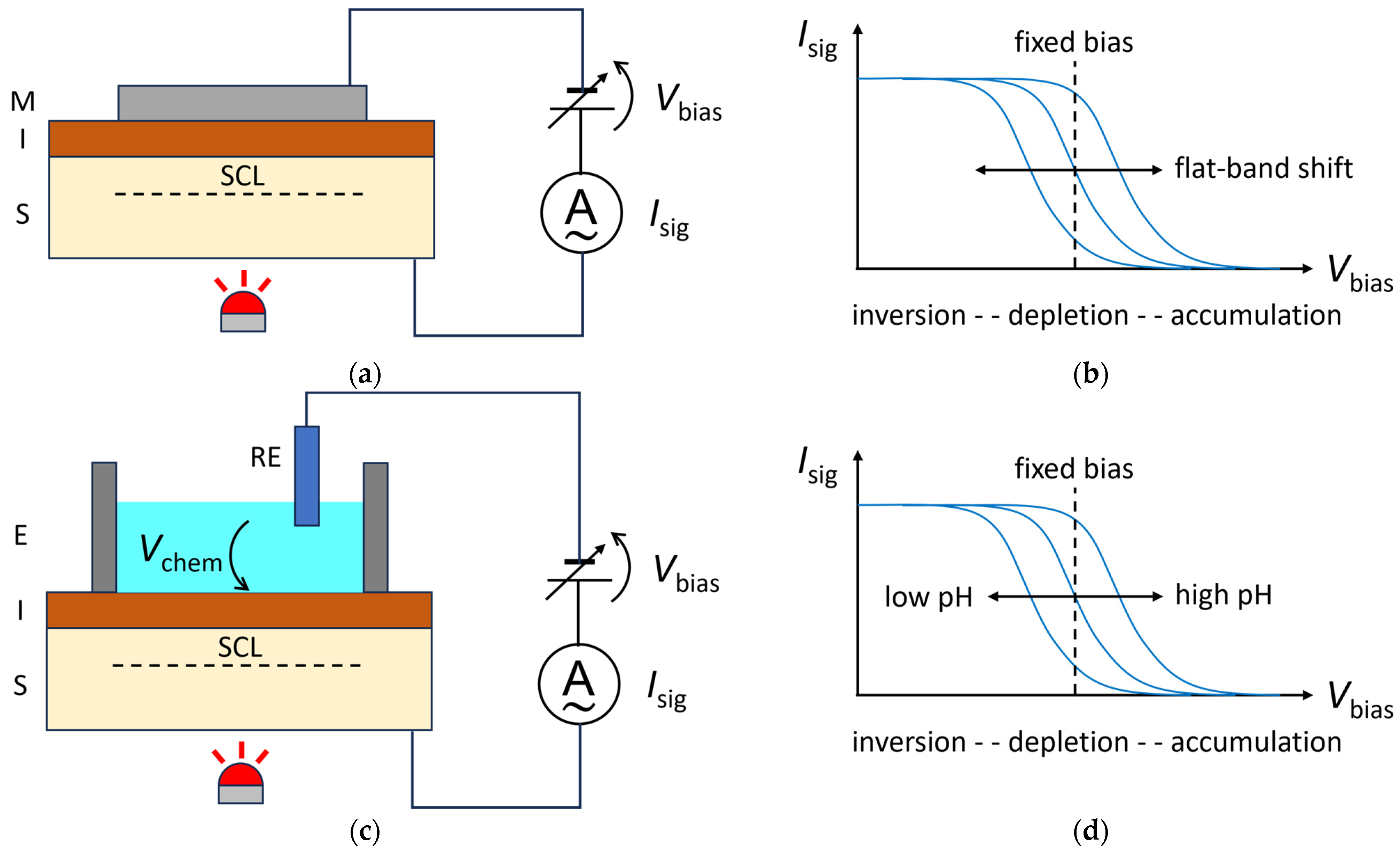
Figure 1. Comparison of SLPT (top) and LAPS (bottom) principles. (a) In SLPT, a chopped light beam illuminates an MIS structure under a bias voltage Vbias, and the amplitude of the photocurrent Isig is recorded. (b) The Isig−Vbias curve of SLPT shifts horizontally depending on the flat-band voltage of the MIS structure. Under a fixed value of Vbias, the current signal Isig varies depending on the local value of the flat-band voltage. (c) The sensing surface of a LAPS is the surface of the insulator, which is in contact with the solution under test, forming an electrolyte–insulator–semiconductor (EIS) structure. A potential difference Vchem is built up between the solution and the sensing surface, depending on the activity of the target analyte. The semiconductor layer is illuminated with a chopped light beam to generate the current signal Isig. (d) The Isig−Vbias curve of a LAPS shifts horizontally depending on the activity of the target analyte. Under a fixed value of Vbias, the current signal Isig varies depending on the local value of the activity of the target analyte.
The operating principle of a LAPS is closely related to that of the SLPT. As shown in Figure 1c, a LAPS consists of a semiconductor plate covered with an insulator, and its surface is in contact with the solution under test, forming an electrolyte–insulator–semiconductor (EIS) structure, which is common to the gate region of an ion-sensitive field-effect transistor (ISFET) [10]. The surface of the insulator layer serves as the sensing surface, typically by selectively capturing the target ions, which builds up a potential difference Vchem between the solution and the sensing surface, as shown in Figure 1c, depending on the activity of the target species. Since Vchem is in series with the externally applied Vbias, their sum will be the effective bias voltage applied to the EIS structure. The measurement process hereafter is identical to that of the SLPT. The semiconductor layer is illuminated by a chopped light beam and the amplitude of the alternating current Isig is measured as a function of Vbias. The horizontal shift in the Isig−Vbias curve represents the change in Vchem, which can be translated into the activity or the concentration of the target ion in the solution. Figure 1d shows an example of a shift in the Isig−Vbias curve of a LAPS that responds to pH changes. As a member of the family of semiconductor-based chemical sensors with a field-effect structure, the LAPS shares many features in common with other such sensors such as the ISFET and capacitive EIS sensor [6]. They have essentially the same response in the surface potential to the activity of target analytes, and the surface modification technologies and materials developed for one can easily be applied to others. In this way, various ions have been measured by a LAPS furnished with ion-selective membranes, and the application of a LAPS to biosensing has also been extensively studied [11][12][13]. For example, enzymes immobilized on a LAPS surface can catalyze a reaction involving the substrate, enabling detection of a pH change. In an affinity-type of biosensing LAPS, the variation in the surface potential due to selective bindings, such as those between antibodies and antigens or even cells, between aptamers and proteins, or between complementary single-stranded DNAs, has been detected successfully.
Artificial olfactory images were realized by applying the SLPT to a gas sensor comprising an MOS structure with a catalytic metal gate [1][2][3]. The history of the development of catalytic field-effect devices, from a hydrogen sensor based on a Pd-gate MOS transistor [14] to electronic noses [15] and artificial olfactory images [1], is described in [3]. In a catalytic field-effect device, the top metal layer in the MOS structure is composed of a catalytic metal, which catalyzes the reaction of the target gas, like hydrogen, on the surface. As a result, a potential difference due to atomic hydrogen is produced at the metal–oxide interface. A variation in this potential difference is observed as a change in the flat-band voltage, which can be read by the SLPT. To obtain an artificial olfactory image as a fingerprint of the gas species, different catalytic metals (Pd, Ir, and Pt) were deposited on the surface, and a temperature gradient was formed along one direction of the sensor plate. In this way, measurements at different positions on the sensing surface can be carried out under different conditions, and therefore, each pixel on the sensing surface can be regarded as an independent sensor that constitutes a large virtual array of sensors, whose output forms the input to the electronic nose system. Examples of artificial olfactory images for different gases such as ammonia, hydrogen, and ethanol were obtained in [1]. These images can be fed as inputs to an electronic nose system or used to train a machine learning system, such as an artificial neural network (ANN), which will be able to recognize and identify unknown gas samples. In [1], the authors also point out the similarity between the proposed method and the olfactory recognition mechanism in our brain, where the signals from olfactory receptor neurons are once encoded into a two-dimensional image.
Whereas a conventional electronic nose system relying on an array of discrete gas sensors can be bulky, an artificial olfactory image can be recorded with a single sensor chip. In addition, as the sensor chip has a temperature gradient in one direction, the response of each catalytic metal at different temperatures is embedded in an artificial olfactory image. The richness of information to be fed into machine learning is an additional benefit of artificial olfactory images.
Kanai et al. [16] applied the same concept to generate taste images. In this electronic tongue system, five different lipid membranes (oleic acid, lecithin, cholesterol, phosphatidyl-ethanolamine, and dioctyl phosphate) were deposited on the sensing surface, which was brought into contact with the sample solution. Photocurrent images were obtained as fingerprints of taste substances such as NaCl for saltiness, HCl for sourness, quinine-HCl for bitterness, saccharose for sweetness, and sodium glutamate monohydrate for umami, as well as several beverages such as coffee, black tea, and beer. Furthermore, Shimizu et al. [17] applied the same technique to biosensing, integrating photopolymer membranes containing enzymes such as urease and glucose oxidase on the sensing surface. Their response was acquired in the form of photocurrent images, which demonstrated the feasibility of monolithically integrated biosensors with a plurality of enzymes.
References
- Lundström, I.; Erlandsson, R.; Frykman, U.; Hedborg, E.; Spetz, A.; Sundgren, H.; Welin, S.; Winquist, F. Artificial ‘olfactory’ images from a chemical sensor using a light pulse technique. Nature 1991, 352, 47–50.
- Winquist, F.; Sundgren, H.; Hedborg, E.; Spetz, A.; Lundström, I. Visual images of gas mixtures produced with field-effect structures. Sens. Actuators B 1992, 6, 157–161.
- Lundström, I.; Svensson, C.; Spetz, A.; Sundgren, H.; Winquist, F. From hydrogen sensors to olfactory images—Twenty years with catalytic field-effect devices. Sens. Actuators B 1993, 13, 16–23.
- Engström, O.; Carlsson, A. Scanned light pulse technique for the investigation of insulator–semiconductor interfaces. J. Appl. Phys. 1983, 54, 5245–5251.
- Hafeman, D.G.; Parce, J.W.; McConnell, H.M. Light-addressable potentiometric sensor for biochemical systems. Science 1988, 240, 1182–1185.
- Yoshinobu, T.; Miyamoto, K.; Werner, C.F.; Poghossian, A.; Wagner, T.; Schöning, M.J. Light-addressable potentiometric sensors for quantitative spatial imaging of chemical species. Annu. Rev. Anal. Chem. 2017, 10, 225–246.
- Liu, Y.; Zhu, P.; Liu, S.; Chen, Y.; Liang, D.; Wang, M.; Du, L.; Wu, C. The Light-addressable potentiometric sensor and its application in biomedicine towards chemical and biological sensing. Chemosensors 2022, 10, 156.
- Meng, Y.; Chen, F.; Wu, C.; Krause, S.; Wang, J.; Zhang, D.-W. Light-addressable electrochemical sensors toward spatially resolved biosensing and imaging applications. ACS Sens. 2022, 7, 1791–1807.
- Luo, J.; Liu, S.; Chen, Y.; Tan, J.; Zhao, W.; Zhang, Y.; Li, G.; Du, Y.; Zheng, Y.; Li, X.; et al. Light addressable potentiometric sensors for biochemical imaging on microscale: A review on optimization of imaging speed and spatial resolution. ACS Omega 2023, 8, 42028–42044.
- Bergveld, P. Development of an ion-sensitive solid-state device for neurophysiological measurements. IEEE Trans. Biomed. Eng. 1970, 17, 70–71.
- Wagner, T.; Schöning, M.J. Light-addressable potentiometric sensors (LAPS): Recent trends and applications. In Electrochemical Sensor Analysis; Alegret, S., Merkoçi, A., Eds.; Elsevier: Amsterdam, The Netherlands, 2007; pp. 87–128.
- Liang, T.; Qiu, Y.; Gan, Y.; Sun, J.; Zhou, S.; Wan, H.; Wang, P. Recent developments of high-resolution chemical imaging systems based on light-addressable potentiometric sensors (LAPSs). Sensors 2019, 19, 4294.
- Yoshinobu, T.; Schöning, M.J. Light-addressable potentiometric sensors for cell monitoring and biosensing. Curr. Opin. Electrochem. 2021, 28, 100727.
- Lundström, I.; Shivaraman, M.S.; Svensson, C.M. A hydrogen-sensitive Pd-gate MOS transistor. J. Appl. Phys. 1975, 6, 3876–3881.
- Sundgren, H.; Lundström, I.; Winquist, F.; Lukkari, I.; Carlsson, R.; Wold, S. Evaluation of multiple gas mixture with a simple MOSFET gas sensor array and pattern recognition. Sens. Actuators B 1990, 2, 115–123.
- Kanai, Y.; Shimizu, M.; Uchida, H.; Nakahara, H.; Zhou, C.G.; Maekawa, H.; Katsube, T. Integrated taste sensor using surface photovoltage technique. Sens. Actuators B 1994, 20, 175–179.
- Shimizu, M.; Kanai, Y.; Uchida, H.; Katsube, T. Integrated biosensor employing a surface photovoltage technique. Sens. Actuators B 1994, 20, 187–192.
More
Information
Subjects:
Engineering, Chemical
Contributors
MDPI registered users' name will be linked to their SciProfiles pages. To register with us, please refer to https://encyclopedia.pub/register
:
View Times:
559
Revisions:
2 times
(View History)
Update Date:
04 Feb 2024
Table of Contents


Notice
You are not a member of the advisory board for this topic. If you want to update advisory board member profile, please contact office@encyclopedia.pub.
OK
Confirm
Only members of the Encyclopedia advisory board for this topic are allowed to note entries. Would you like to become an advisory board member of the Encyclopedia?
Yes
No
${ textCharacter }/${ maxCharacter }
Submit
Cancel
Back
Comments
${ item }
|
${ item.createdUser.fullName }
${ item.createdAt }
${ item.vote }
${ item.reply }
Delete
${ reply.createdUser.fullName }
${ reply.createdAt }
${ reply.vote }
Delete
There is no reply to this comment~
${ item.replyTextCharacter }/${ item.replyMaxCharacter }
Submit
Cancel
More
No more~
There is no comment~
${ textCharacter }/${ maxCharacter }
Submit
Cancel
${ selectedItem.replyTextCharacter }/${ selectedItem.replyMaxCharacter }
Submit
Cancel
Confirm
Are you sure to Delete?
Yes
No