Your browser does not fully support modern features. Please upgrade for a smoother experience.
Submitted Successfully!
 +1 credit
Thank you for your contribution! You can also upload a video entry or images related to this topic.
For video creation, please contact our Academic Video Service.
| Version | Summary | Created by | Modification | Content Size | Created at | Operation |
|---|---|---|---|---|---|---|
| 1 | Daquan Yu | -- | 2204 | 2024-01-17 11:48:04 | | | |
| 2 | Sirius Huang | Meta information modification | 2204 | 2024-01-18 01:56:45 | | |
Video Upload Options
We provide professional Academic Video Service to translate complex research into visually appealing presentations. Would you like to try it?
Cite
If you have any further questions, please contact Encyclopedia Editorial Office.
Yu, C.; Wu, S.; Zhong, Y.; Xu, R.; Yu, T.; Zhao, J.; Yu, D. Application of Through Glass Via Technology. Encyclopedia. Available online: https://encyclopedia.pub/entry/53970 (accessed on 12 July 2026).
Yu C, Wu S, Zhong Y, Xu R, Yu T, Zhao J, et al. Application of Through Glass Via Technology. Encyclopedia. Available at: https://encyclopedia.pub/entry/53970. Accessed July 12, 2026.
Yu, Chen, Shaocheng Wu, Yi Zhong, Rongbin Xu, Tian Yu, Jin Zhao, Daquan Yu. "Application of Through Glass Via Technology" Encyclopedia, https://encyclopedia.pub/entry/53970 (accessed July 12, 2026).
Yu, C., Wu, S., Zhong, Y., Xu, R., Yu, T., Zhao, J., & Yu, D. (2024, January 17). Application of Through Glass Via Technology. In Encyclopedia. https://encyclopedia.pub/entry/53970
Yu, Chen, et al. "Application of Through Glass Via Technology." Encyclopedia. Web. 17 January, 2024.
Copy Citation
Glass has emerged as a highly versatile substrate for various sensor and MEMS (microelectromechanical systems) packaging applications, including electromechanical, thermal, optical, biomedical, and RF devices, due to its exceptional properties such as high geometrical tolerances, outstanding heat and chemical resistance, excellent high-frequency electrical properties, and the ability to be hermetically sealed. In these applications, Through Glass Via (TGV) technology plays a vital role in manufacturing and packaging by creating electrical interconnections through glass substrates.
Through Glass Via
MEMS sensors
sensor manufacturing
sensor packaging
1. Introduction
Due to the progress of 5G, smart cars, medical gadgets, and other industries, electronic products are designed to be more portable and convenient. Much research has been invested in the fabrication, integration, and packaging of sensors, aiming to improve performance and dependability and cut down costs. The packaging of MEMS sensors can constitute up to 30% of the cost of producing a device [1], and the sealing capacity and interconnectivity significantly impact device performance, which subsequently affects the production and application of sensors. Wafer-level packaging, exhibiting manufacturing efficiency and excellent device performance, has advantages in reducing the size and saving costs compared to device-level packaging [2].
Through Glass Via (TGV) is the vertical electrical interconnection through the glass substrate, which corresponds to TSV. Glass substrates possess superior electrical properties and lower parasitic capacitance than common silicon and SOI substrates, facilitating the extension of high-frequency signal transmission [3]. The excellent optical properties of glass make it more suitable for optical applications such as Micro-Opto-Electro-Mechanical Systems (MOEMS) [4]. Adjusting the composition of the glass and optimizing surface treatments can modify the coefficient of thermal expansion (CTE) and mechanical strength of the substrate. This results in improved metal adhesion, stress control, and reliability [5][6]. TGV technology supports a wide range of thicknesses (from 50 µm to 900 µm) and large wafer sizes (from 6″ to 12″) and panels (from 510 × 515 mm to 1500 × 800 mm). The glass-based process is more straightforward, without the need to deposit an insulating layer on the inner wall of the TGV, making the manufacturing cost of glass package substrates much lower than that of silicon substrates. Glass can be bonded to substrates, including silicon and other glasses, using techniques such as anodic bonding and direct bonding. These methods create a stable vacuum environment suitable for inertial sensors like accelerometers and gyroscopes [1][2][5][7][8][9][10][11]. The TGV process provides the fabrication and metallization of high-density, high-aspect-ratio glass vias, enabling a reduction in device size while maintaining high-performance electrical interconnects. Intel says glass substrate technology can increase the chip area in a single package by 50%, allowing more chiplets to be crammed in. It reduces the thickness by about half compared to ABF plastic, providing higher signaling speeds and power efficiencies [12].
2. Application of TGV for Sensors’ Manufacturing and Packaging
Packaging serves to isolate sensitive and fragile internal and external environments, protect internal space, and facilitate signal transmission. The cost of packaging MEMS sensors accounts for more than 30% of the total manufacturing cost. The optimization and enhancement of the packaging process can assist the sensors in achieving superior performance whilst reducing costs.
The packaging process is essential for sensors, particularly MEMS sensors. Wafer bonding technology and vertical interconnect technology are the key technologies for wafer-level packaging technology, which is of great value in achieving a smaller device size, lower manufacturing cost, and lower power consumption [10]. Glass has been widely used in sensors’ packaging due to its unique properties such as high mechanical stability, high sealing performance, high transparency, and low thermal conductivity. It can serve as a cap substrate to create a highly vacuum-sealed environment through anodic bonding, direct bonding, or metal bonding with silicon, SOI, glass, or other substrates in sensor packaging. Moreover, the development of TGV technology, mainly including vias’ formation and metallization, has made glass substrates more preferred in sensor packaging due to their superior performance advantages. As shown in Figure 1, this section provides detailed information on the application and performance of the TGV process for different types of sensors according to the performances of glass.
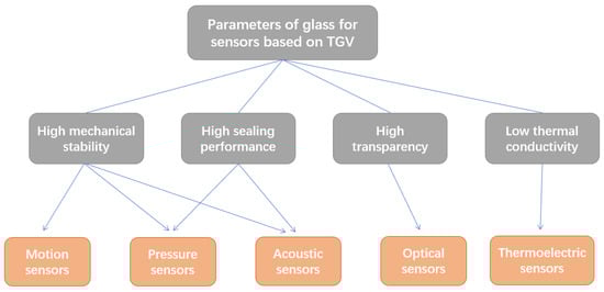
Figure 1. Parameters of glass for sensors based on TGV technology.
2.1. Motion Sensors
Motion sensors are typically used for motion detection and acceleration measurement. Chips require sufficient impact resistance to protect the internal microstructure. Glass has strong mechanical properties that can improve the impact resistance of sensors. TGV technology has great potential for motion sensing applications.
Ma et al. [5] used a glass adapter plate as a top cover to solve the stress problem of TSV technology. A symmetrical sandwich structure for MEMS inertial sensors based on the bulk silicon process was constructed. Blind vias were formed on a 400 µm thick glass substrate by powder blasting, and TGVs were formed by backside grinding and polishing. Al was deposited by sputtering to provide electrical interconnections in the TGVs. A redistribution layer was formed on both sides of the adapter plate by photolithography. BCB was used as an adhesive layer to bond the adapter plate to the MEMS accelerometer wafer for the wafer-level packaging of the accelerometer.
Fu et al. [7] proposed a comb structure accelerometer, in which the glass cover plate with TGV was bonded to the accelerometer anode to form a sealing and interconnection structure. Laser ablation was used to create square vias with 300 µm thickness on BF33 glass. The TGV-metallization process was performed using metal mold method [13]. Yang et al. [8] used the powder blasting method to fabricate biconical vias with a diameter of about 600 µm on a 500 µm thick glass substrate. Cr/Cu was sputtered onto the substrate as a seed layer, which was then filled with TGVs through a PPR copper plating process. Following polishing, the TGV substrate was obtained, from which shock threshold sensors were fabricated. During testing, reliable switching signals were obtained at a shock velocity of 1000 g.
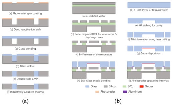
Yang et al. [2] processed Pyrex 7740 glass using a picosecond laser at a wavelength of 532 nm and obtained vias with an entrance diameter of 90 µm, an exit diameter of 48 µm, and a depth of 300 µm. Vertical electrical interconnections were achieved using electron beam evaporated metal filler to cover the inside of the TGV, and the TGV substrate was bonded to the gyroscope to complete the package. The devices were tested to maintain a vacuum of 1 Pa for over two years. Zhang et al. [9] fabricated glass caps with low-resistance silicon as the conductive column using a glass reflow process and completed the hermetic encapsulation of the capacitive gyroscope by anodic bonding. The quality factor of the tested device exceeded 220,000, which is an order of magnitude greater than that of the unencapsulated gyroscope; the process flow of glass caps is shown in Figure 2a. Kuang et al. [2][10][11] conducted an initial investigation into the process mechanism of glass reflow, followed by the successful sealing of a gyroscope using this method. This proved the feasibility of wafer-level vacuum packaging using TGV technology in combination with triple-anode bonding.
2.2. Pressure Sensors
Pressure sensors can be categorized as capacitive pressure sensors, piezoelectric pressure sensors, or resonant pressure sensors, which can be used in aerospace inspection and atmospheric pressure sensing. These sensors are typically vacuum-sealed, such as micro-resonators, where the mechanical quality factor deteriorates with increasing ambient pressure due to air damping effects. The potential of the TGV process for applications such as capacitive pressure sensors has been demonstrated. Haque et al. [15] produced capacitive pressure sensors using the glass reflow method. The wafer was heated inside a tube furnace, and the grooves were filled with melted glass to form silicon conductive vias. This process completed the sealing of the sensor and provided electrical lead-in, eliminating the need to install bond wires on the front.
Kim et al. [16] used glass reflow technology to fabricate silicon–glass structured wafers for electrical interconnects, proving that glass provides good electrical isolation and minimizes parasitic capacitance. Zhenyu et al. [14] used laser drilling in Pyrex 7740 glass to fabricate glass caps. The resonant pressure sensors were fabricated by combining glass caps with TGVs on SOI wafers. The glass cap with TGV achieved both vacuum sealing and electrical lead-out, which can be seen in Figure 2b. The manufactured micro-pressure sensor was verified to have a Q-factor greater than 22,000 and was stable for 5 months, confirming the reliability of the vacuum package and electrical connection.
2.3. Acoustic Sensors
Changes in the external environment (such as temperature, pressure, humidity, etc.) have an impact on the properties of sensor materials, thereby affecting the propagation characteristics of sound waves (mainly the sound speed). By utilizing this principle, changes in the sound speed can be detected to determine changes in the external environment.
Chen et al. [17] designed a new three-dimensional wafer-level packaging (3-D WLP) solution to improve the performance and reliability of surface acoustic wave (SAW) filter packages with large cavities. Glass capping and vertical interconnects were realized using TGV, which can avoid the outgassing problem and prevent the contamination of the interdigital transducers (IDTs).
The application of TGV technology in acoustic sensors is still relatively limited, mainly focusing on CMUT. Ultrasonic transducers have potential applications in the medical and underwater exploration fields [18]. Capacitive micromachined ultrasonic transducers (CMUTs) offer an alternative to piezoelectric technology for producing two-dimensional ultrasonic transducer arrays with typical integrated circuit manufacturing processes. CMUT arrays can be integrated with front-end ICs through flip-chip bonding and TSV processing. TSV processing is a complex procedure with high parasitic capacitance and roughness, which can cause additional stress and degrade CMUT performance. As a result, TGV technology presents itself as a promising alternative.
Zhang et al. [19] developed a procedure to create vacuum-sealed CMUTs through anodic bonding on borosilicate glass substrates. They then extended this process using TGV interconnects. Laser ablation was employed to generate via holes, with 70 µm diameter at the entry and 50 µm at the exit on 700 µm thick borosilicate glass. Copper paste was used to fill the vias, which were subsequently sintered and polished to form the TGVs. CMUT array fabrication was completed, and performance tests were conducted to demonstrate the devices’ basic functionality, although they were not vacuum-sealed. Zhang et al. [3][19][20] reported a fabrication process for vacuum-sealed CMUTs on borosilicate glass substrates using anodic bonding and completed the fabrication process. A process of fabricating using sacrificial etching was demonstrated to overcome the restriction of employing glass substrates that are compatible with anodic bonding.
2.4. Optical Sensors
There are still limited optical components and systems utilizing the wafer-level packaging method. Glass, which has remarkable optical and electrical characteristics, is particularly appropriate for packaging optical sensors. Brusberg et al. [21][22] used a laser drilling process to fabricate TGVs in D263T glass for 3D interconnections and integrated Mach-Zehnder interferometer (MZI) waveguides, fluidic channels, optoelectronic elements, and silicon dies to form optical sensor. Stenchly et al. [4] introduced a modular packaging system suitable for optical components and systems. The system comprised a TGV interposer and a glass cover plate. A specialized process can fabricate an optical window on the glass cover plate, achieving tilting by way of structural tilting through thermally induced stresses during high-temperature baking. TGV adaptor plates can be integrated into a glass adaptor plate body through techniques like glass reflow, with low-resistance silicon or copper serving as the interconnect material. Optical sensors or laser diodes can be packaged by bonding the glass cover plate and adapter plate. This modular design has sizable industrial potential and can be utilized in various applications.
2.5. Thermoelectric Sensors
Based on the adjustable thermal conductivity, glass has attracted considerable attention in the application of thermoelectric sensors. Thermoelectric sensors can convert temperature changes into electrical changes, allowing them to be applied to fabricate thermoelectric generators and wind sensors.
Thermoelectric generators can transform temperature difference or low-grade waste heat into electricity. This has a great application prospect in portable electronics, wireless sensors, and medical devices. As glass boasts low thermal conductivity, it can effectively increase the temperature difference between the hot and cold ends of micro-thermocouples, enhancing the thermoelectric conversion capability, in combination with high-aspect-ratio TGVs. Liu et al. [23] fabricated micro-thermoelectric generators based on Bi2Te3 and Sb2Te3 using 200 µm thick glass substrates. The vias were formed by laser ablation, and Bi2Te3 and Sb2Te3 were deposited in the vias at both ends of the device. The 200 µm thick glass was capable of generating a temperature difference of 138 K, which, in turn, provided an output voltage of 40.89 mV and an output power of 19.72 µW. Compared to photoresist masks, thermal sensors produced on glass substrates offer technical and cost benefits by allowing for more flexible control of the device’s output voltage and power. Wind sensors are commonly used in areas such as agricultural production, transportation, and energy harvesting. The wind force can be estimated by detecting subtle temperature changes caused by the wind with sensors. Miniaturized hot air sensors offer high initial sensitivity and low processing costs, but their reliance on heating for measurement results in high energy consumption. Glass is a low-thermal-conductivity material that can effectively reduce heat loss. Relying on TGV technology allows for electrical connections without the need for external wiring, meeting the requirements of reliability and high performance. Zhu et al. [24][25][26][27] proposed a thermal wind sensor packaging scheme, implemented using glass reflow technology. Drawing upon the performance benefits of the glass substrate and TGVs, the total heating power consumption of the sensor amounted to a mere 14.5 mW.
References
- Yang, F.; Han, G.; Yang, J.; Zhang, M.; Ning, J.; Yang, F.; Si, C. Research on Wafer-Level MEMS Packaging with Through-Glass Vias. Micromachines 2018, 10, 15.
- Kuang, Y.B.; Hou, Z.Q.; Zhuo, M.; Xu, Q.; Li, Q.S.; Xiao, B.; Shan, H.; Xiao, D.B.; Wu, X.Z. Research of Wafer-Level Vacuum Packaging Based on TGV Technology for MEMS Devices. In Proceedings of the 33rd IEEE International Conference on Micro Electro Mechanical Systems (MEMS), Vancouver, BC, Canada, 18–22 January 2020; pp. 988–991.
- Adelegan, O.J.; Coutant, Z.A.; Zhang, X.; Yamaner, F.Y.; Oralkan, O. A 2D Capacitive Micromachined Ultrasonic Transducer (CMUT) Array with Through-Glass-Via Interconnects Fabricated Using Sacrificial Etching Process. In Proceedings of the IEEE International Ultrasonics Symposium (IUS), Glasgow, UK, 6–9 October 2019; pp. 1205–1208.
- Stenchly, V.; Reinert, W.; Quenzer, H.J. Modular packaging concept for MEMS and MOEMS. In Proceedings of the 28th Micromechanics and Microsystems Europe Workshop (MME), Uppsala, Sweden, 23–25 August 2017.
- Ma, S.L.; Ren, K.L.; Xia, Y.M.; Yan, J.; Luo, R.F.; Cai, H.; Jin, Y.F.; Ma, M.J.; Jin, Z.H.; Chen, J. Process Development of a New TGV Interposer for Wafer Level Package of Inertial MEMS Device. In Proceedings of the 17th International Conference on Electronic Packaging Technology (ICEPT), Wuhan, China, 16–19 August 2016; pp. 983–987.
- Wang, Y.X.; Ma, S.L.; Liu, X.Q.; Zhao, J.H. Partially filled TGV based on Double Sides Cu Conformal Electroplating Process for MEMS Vacuum Packaging. In Proceedings of the International Conference on Electronics Packaging (ICEP), Sapporo, Japan, 11–14 May 2022; pp. 53–54.
- Fu, Y.C.; Han, G.W.; Gu, J.B.; Zhao, Y.M.; Ning, J.; Wei, Z.Y.; Yang, F.H.; Si, C.W. A High-Performance MEMS Accelerometer with an Improved TGV Process of Low Cost. Micromachines 2022, 13, 1071.
- Yang, Z.; Wang, Y.; Wang, H.; Wang, Y.; Dai, X.; Ding, G.; Zhao, X. High-g MEMS shock threshold sensor integrated on a copper filling through-glass-via (TGV) substrate for surface mount application. In Proceedings of the 18th International Conference on Solid-State Sensors, Actuators and Microsystems (TRANSDUCERS), Anchorage, AK, USA, 21–25 June 2015; pp. 291–294.
- Zhang, M.; Yang, J.; He, Y.R.; Yang, F.; Yang, F.H.; Han, G.W.; Si, C.W.; Ning, J. Research on a 3D Encapsulation Technique for Capacitive MEMS Sensors Based on Through Silicon Via. Sensors 2019, 19, 93.
- Kuang, Y.B.; Xiao, D.B.; Zhou, J.; Li, W.Y.; Hou, Z.Q.; Cui, H.J.; Wu, X.Z. Theoretical model of glass reflow process for through glass via (TGV) wafer fabrication. J. Micromech. Microeng. 2018, 28, 095004.
- Kuang, Y.B.; Xiao, D.B.; Zhou, J.; Zhuo, M.; Li, W.Y.; Hou, Z.Q.; Cui, H.J.; Wu, X.Z. Enhancing airtightness of TGV through regulating interface energy for wafer-level vacuum packaging. Microsyst. Technol. -Micro-Nanosyst.-Inf. Storage Process. Syst. 2018, 24, 3645–3649.
- Intel Shows off Work on Next-Gen Glass Core Substrates, Plans Deployment Later in Decade. Available online: https://www.anandtech.com/show/20058/intel-shows-off-glass-core-substrate-plans-deployment-late-decade (accessed on 18 September 2023).
- Gu, J.B.; Xia, X.Y.; Zhang, W.B.; Li, X.X. A Modified MEMS-Casting Based TSV Filling Method with Universal Nozzle Piece That Uses Surface Trenches as Nozzles. In Proceedings of the 19th International Conference on Electronic Packaging Technology (ICEPT), Shanghai, China, 8–11 August 2018; pp. 536–539.
- Luo, Z.; Chen, D.; Wang, J.; Li, Y.; Chen, J. A High-Q Resonant Pressure Microsensor with Through-Glass Electrical Interconnections Based on Wafer-Level MEMS Vacuum Packaging. Sensors 2014, 14, 24244–24257.
- Kim, J.-K.; Baek, C.-W. Capacitive pressure sensor with wafer-through silicon vias using SOI-Si direct wafer bonding and glass reflow technique. IEICE Electron. Express 2013, 10, 20130453.
- Haque, R.-u.M.; Wise, K.D. A Glass-in-Silicon Reflow Process for Three-Dimensional Microsystems. J. Microelectromechanical Syst. 2013, 22, 1470–1477.
- Chen, Z.H.; Yu, D.Q.; Jiang, F. Development of 3-D Wafer Level Packaging for SAW Filters Using Thin Glass Capping Technology. IEEE Trans. Compon. Packag. Manuf. Technol. 2022, 12, 375–381.
- Herickhoff, C.D.; van Schaijk, R. cMUT technology developments. Z. Fur Med. Phys. 2023, 33, 256–266.
- Zhang, X.; Yamaner, F.Y.; Oralkan, O.; IEEE. Fabrication of Capacitive Micromachined Ultrasonic Transducers with Through-Glass-Via Interconnects. In Proceedings of the IEEE International Ultrasonics Symposium (IUS), Taipei, Taiwan, 21–24 October 2015.
- Adelegan, O.J.; Coutant, Z.A.; Zhang, X.; Yamaner, F.Y.; Oralkan, O. Fabrication of 2D Capacitive Micromachined Ultrasonic Transducer (CMUT) Arrays on Insulating Substrates with Through-Wafer Interconnects Using Sacrificial Release Process. J. Microelectromechanical Syst. 2020, 29, 553–561.
- Brusberg, L.; Schröder, H.; Töpper, M.; Arndt-Staufenbiel, N.; Röder, J.; Lutz, M.; Reichl, H. Thin Glass Based Packaging Technologies for Optoelectronic Modules. In Proceedings of the 59th Electronic Components and Technology Conference, San Diego, CA, USA, 26–29 May 2009; pp. 207–212.
- Brusberg, L.; Schröder, H.; Töpper, M.; Reichl, H. Photonic System-in-Package Technologies Using Thin Glass Substrates. In Proceedings of the 11th Electronics Packaging Technology Conference, Singapore, 9–11 December 2009; pp. 930–935.
- Liu, S.; Hu, B.; Liu, D.; Li, F.; Li, J.-F.; Li, B.; Li, L.; Lin, Y.-H.; Nan, C.-W. Micro-thermoelectric generators based on through glass pillars with high output voltage enabled by large temperature difference. Appl. Energy 2018, 225, 600–610.
- Zhu, Y.Q.; Chen, B.; Qin, M.; Huang, J.Q.; Huang, Q.A. A Self-packaged Self-heated Thermal Wind Sensor with High Reliability and Low Power Consumption. In Proceedings of the IEEE 10th International Conference on Nano/Micro Engineered and Molecular Systems (NEMS), Xi’an, China, 7–11 April 2015; pp. 193–196.
- Zhu, Y.Q.; Chen, B.; Qin, M.; Huang, Q.A.; Huang, J.Q. Development of A Robust 2-D Thermal Wind Sensor Using Glass Reflow Process for Low Power Applications. In Proceedings of the IEEE 65th Electronic Components and Technology Conference (ECTC), San Diego, CA, USA, 26–29 May 2015; pp. 1633–1639.
- Zhu, Y.Q.; Chen, B.; Gao, D.; Qin, M.; Huang, Q.A.; Huang, J.Q. A robust and low-power 2-D thermal wind sensor based on a glass-in-silicon reflow process. Microsyst. Technol. -Micro-Nanosyst. -Inf. Storage Process. Syst. 2016, 22, 151–162.
- Zhu, Y.Q.; Qin, M.; Ye, Y.Z.; Yi, Z.X.; Long, K.W.; Huang, Q.A. Modelling and characterization of a robust, low-power and wide-range thermal wind sensor. Microsyst. Technol.-Micro-Nanosyst. -Inf. Storage Process. Syst. 2017, 23, 5571–5585.
More
Information
Subjects:
Physics, Mathematical
Contributors
MDPI registered users' name will be linked to their SciProfiles pages. To register with us, please refer to https://encyclopedia.pub/register
:
View Times:
1.6K
Revisions:
2 times
(View History)
Update Date:
18 Jan 2024
Table of Contents


Notice
You are not a member of the advisory board for this topic. If you want to update advisory board member profile, please contact office@encyclopedia.pub.
OK
Confirm
Only members of the Encyclopedia advisory board for this topic are allowed to note entries. Would you like to become an advisory board member of the Encyclopedia?
Yes
No
${ textCharacter }/${ maxCharacter }
Submit
Cancel
Back
Comments
${ item }
|
${ item.createdUser.fullName }
${ item.createdAt }
${ item.vote }
${ item.reply }
Delete
${ reply.createdUser.fullName }
${ reply.createdAt }
${ reply.vote }
Delete
There is no reply to this comment~
${ item.replyTextCharacter }/${ item.replyMaxCharacter }
Submit
Cancel
More
No more~
There is no comment~
${ textCharacter }/${ maxCharacter }
Submit
Cancel
${ selectedItem.replyTextCharacter }/${ selectedItem.replyMaxCharacter }
Submit
Cancel
Confirm
Are you sure to Delete?
Yes
No