Submitted Successfully!
To reward your contribution, here is a gift for you: A free trial for our video production service.
Thank you for your contribution! You can also upload a video entry or images related to this topic.
Version Summary Created by Modification Content Size Created at Operation
1 -- 2322 2024-01-12 03:12:21 |
2 layout -5 word(s) 2317 2024-01-12 04:03:04 |

Video Upload Options

Do you have a full video?

Confirm

Are you sure to Delete?
Cite
If you have any further questions, please contact Encyclopedia Editorial Office.
Jin, G.; Kim, S.; Han, H. Synthesis Methodologies of Topological Nanomaterials. Encyclopedia. Available online: https://encyclopedia.pub/entry/53768 (accessed on 19 May 2024).
Jin G, Kim S, Han H. Synthesis Methodologies of Topological Nanomaterials. Encyclopedia. Available at: https://encyclopedia.pub/entry/53768. Accessed May 19, 2024.
Jin, Gangtae, Seo-Hyun Kim, Hyeuk-Jin Han. "Synthesis Methodologies of Topological Nanomaterials" Encyclopedia, https://encyclopedia.pub/entry/53768 (accessed May 19, 2024).
Jin, G., Kim, S., & Han, H. (2024, January 12). Synthesis Methodologies of Topological Nanomaterials. In Encyclopedia. https://encyclopedia.pub/entry/53768
Jin, Gangtae, et al. "Synthesis Methodologies of Topological Nanomaterials." Encyclopedia. Web. 12 January, 2024.
Synthesis Methodologies of Topological Nanomaterials
Edit

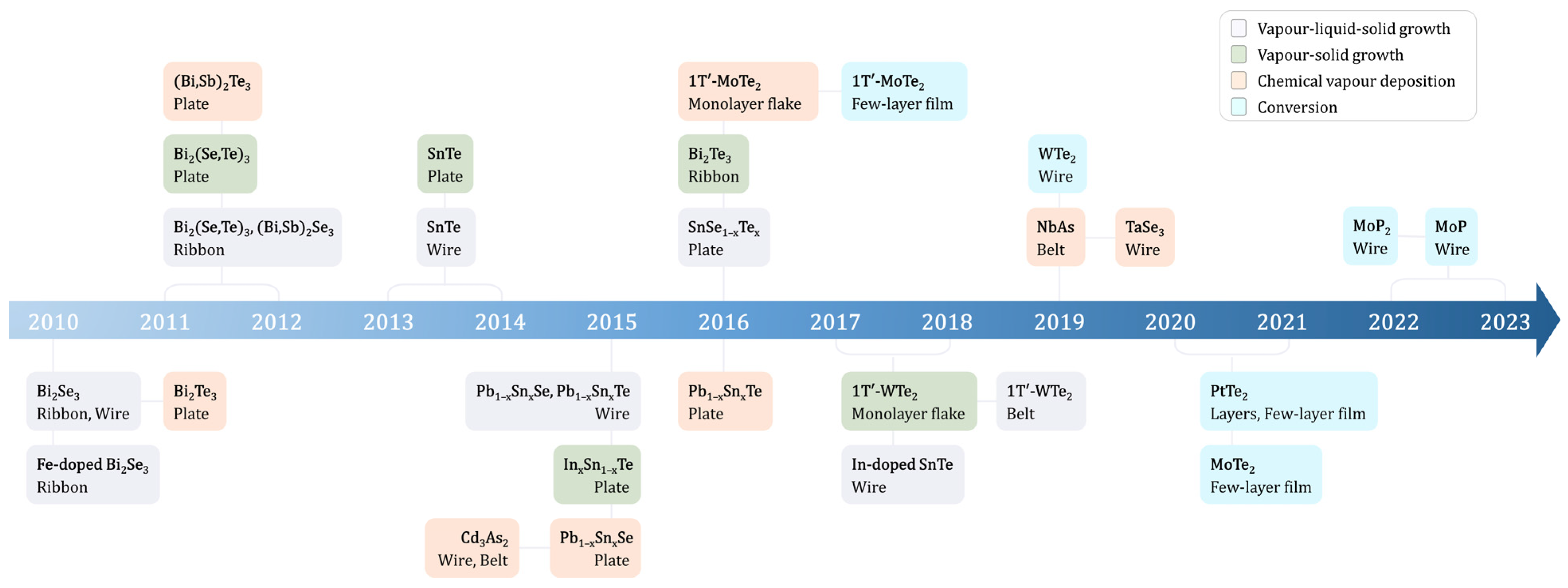
The discovery of topological materials has opened up new areas in condensed matter physics. These materials are noted for their distinctive electronic properties, unlike conventional insulators and metals. This discovery has not only spurred new research areas but also offered innovative approaches to electronic device design. A key aspect of these materials is now that transforming them into nanostructures enhances the presence of surface or edge states, which are the key components for their unique electronic properties. Synthesis methods are discussed, including vapor–liquid–solid (VLS) growth, chemical vapor deposition (CVD), and chemical conversion techniques. Moreover, the scaling down of topological nanomaterials has revealed new electronic and magnetic properties due to quantum confinement.

topological materials nanostructures synthesis

1. Introduction

To harness the potential of topological materials in electronics, it is essential to precisely manage and detect their states in nanostructures [1][2]. Nanostructures can amplify topological states due to their significantly large surface area-to-volume ratio, enhancing the contribution of the topological surface or edge states. This research delves into the synthesis of topological nanostructures ranging from topological insulators to semimetal/metal nanostructures of the Weyl and Dirac types and their application in electronics.
In the past decade, the field of condensed matter physics has seen the emergence of a novel class of materials known as topological materials [3]. These materials, characterized by their unique electronic band structures, diverge significantly from conventional insulators and metals [4][5][6]. Their distinct band topology gives rise to the robust, helical transport of the electrons, exhibiting a linear energy–momentum relationship at the material’s edge or surface. These materials exhibit topologically protected surface states that bring exotic electronic properties. In topological insulators (TIs), these surface states result from the inversion of the bulk bands due to the strong spin–orbit coupling and are protected by time reversal symmetry. The scope of topological materials has recently expanded to encompass topological semimetals (TSMs), notably Weyl and Dirac semimetals [7]. Weyl and Dirac semimetals are three-dimensional (3D) systems with gapless bulk states consisting of relativistic chiral fermions close to nodal points and Fermi arc surface states. The 3D Weyl and Dirac equations describe these systems, respectively. The early development of topological materials, including experimental and theoretical findings to TIs, and TSMs, have been extensively covered in several review articles [2][8][9][10][11][12].
Topologically protected surface states in materials provide attractive electronic properties for future advanced electronic applications. For example, the linear dispersion between momentum and energy in these materials is promising for high-speed electronics, as it allows for faster electron transport [13][14][15]. Additionally, the locking of spin and momentum in topological materials makes them ideal for spintronics, which involves the manipulation of electron spins for information storage and processing [16][17][18][19][20]. Furthermore, the directional motion of electrons in topological materials can enable the development of low-dissipation electronics, reducing energy loss and improving efficiency [21][22][23]. These advantages make topological materials highly attractive for advanced electronic applications. These distinct characteristics of the topological surface states have been extensively studied in bulk systems through surface-sensitive techniques; nevertheless, these properties have not been thoroughly studied in nanostructures [24][25][26][27][28].
Investigating the topological surface states within nanostructures offers a significant advantage, as the nanostructures enhance the role of the topological surface state transport and minimize the effect of bulk electronic states in transport measurements. Many TIs and TSMs have been successfully transformed into nanostructures. In early studies of layered TIs, Bi2Se3 and Bi2Te3 were achieved through direct synthesis or mechanical exfoliation. This transformation has broadened the horizons of quantum computing and spintronics. The reduced scaling of these materials allows unique quantum confinement effects [29][30], leading to new electronic and magnetic properties [18].
Among the various techniques mentioned, the vapor–liquid–solid (VLS) method is particularly favored for its ability to produce high-quality, single-crystalline nanostructures. On the other hand, chemical vapor deposition (CVD) offers scalability and versatility, making it suitable for large-scale production. Conversion methods, while less prevalent, provide an alternative route for obtaining topological nanomaterials from preexisting structures. The selection of a synthesis method is crucial, since it can significantly influence the quality, morphology, and properties of the resulting topological nanomaterials.

2. Synthesis Methodologies 

Numerous TIs and TSMs have been transformed into nanostructures. While some are derived from bulk layered crystals via mechanical exfoliation, researchers' focus here is on their direct synthesis. The VLS and CVD growth techniques are the predominant methods employed for crafting these nanostructures, especially for studying electrical transport attributes. Figure 1 provides a comprehensive timeline of the significant achievements in synthesizing nanomaterials, including topological insulators (TIs) and topological crystalline insulators (TCIs), as well as Weyl and Dirac semimetals.
Figure 1. Timeline of the development of topological nanomaterials with various synthesis methods, such as vapor–liquid–solid, chemical vapor deposition growth, and conversion techniques.
In the realm of experimental demonstrations, the exploration of topological materials has predominantly centered around their bulk forms, achieved through specialized single-crystal growth techniques. These methods include Bridgman growth, the Czochralski method, the floating zone technique, and chemical vapor transport (CVT) [31]. These techniques have traditionally yielded high-quality single crystals of topological materials [32][33][34], revealing valuable insights into their unique topology and band structures. However, there are notable challenges with these traditional single-crystal growth methods, including difficulties in easily integrating them into nanoscale devices with moderate processing temperatures, achieving high conformality, and controlling nucleation and crystallizations on arbitrary interfaces. This is particularly true when producing nanostructured forms of scalable topological materials. Consequently, the potential applications of topological materials in the domain of quantum computation and other cutting-edge technologies have been hindered by a practical gap in controlled fabrication.
To control nanoscale crystallization, nanostructured topological materials can be confined one-dimensionally (1D) using VLS growth [1]. In VLS growth, metal nanoparticles, often composed of gold, act as catalysts to initiate growth. Source materials in a vapor phase are introduced into the system in a CVD process. When the growth temperature is reached, the metal catalyst enters a liquid state, causing gas phase atoms of the precursor to dissolve into the liquid metal particles. As the concentration of precursor atoms in the liquid metal becomes higher than the thermodynamic solubility limit at the growth temperature, these dissolved atoms aggregate and crystallize at one end of the liquid metal particle. By sustaining a constant supply of source vapor, an equilibrium state is achieved. During this phase, the metal particle expels excess dissolved atoms to uphold the solubility limit concentration, consequently extending the nanowire’s length.
A distinctive aspect of VLS growth is that the nanowire’s diameter is precisely dictated by the dimensions of the metal nanoparticle, which is essential to determine the diameter-dependent electron scatterings, especially for evaluating low-dissipation interconnects using TSMs. Cobalt silicide (CoSi) nanowires with a maximum current density of 1.6 × 10⁸ A·cm−2 were grown with a 2 nm thick Au catalyst. An Au–Si eutectic alloy was formed at the growth temperature, serving as a Si source [35]. In diameter confined CoSi slabs with 8~40 atomic layers, the calculated resistance area product of the nanoslabs is significantly lower than that of the bulk. However, contrary to theoretical calculations regarding the surface state’s dominant transport of CoSi nanoslabs [36], the resistivity values of VLS-grown 1D CoSi (326 μΩ·cm) and MOCVD-grown 1D Co-Si NWs (~510 μΩ·cm) without any catalyst exhibited markedly higher values compared to that of the bulk crystal (180 μΩ·cm), despite their high surface-to-volume ratio [35][37].
By manipulating the thickness of the gold catalyst layer below 15 nm, Weyl semimetal Niobium arsenide (NbA) nanobelts were grown, showing a typical width in the range of hundreds of nanometers and a thickness around ~200 nm. An increase in the initial gold thickness to 40 nm only led to the growth of NbA nanowires. In the case of the NbA nanobelts, there was an anomalous resistivity reduction from 35 μΩ·cm (bulk crystals) to 3 μΩ·cm at room temperature, governed by the surface state’s dominant transport. In the nanobelt configuration, the confinement along the z-direction minimally affected the surface transport properties. However, the transformation into NbA nanowires exposed surface carriers to experience boundary scatterings due to strong in-plane confinement, which led to a degradation in mobility and higher sheet resistance (>100 Ω) of the NbA nanobelts with a thickness of ~100 nm. This phenomenon poses challenges for scaling down towards low-resistivity interconnects based on NbAs [38].
The 1D confinement effect may still lead to even richer physics due to the increased contribution from the topological surface states. In the topological crystalline insulator SnTe, 1D confinement affects the ferroelectric transition temperature, as systemically revealed in in situ cryogenic transmission electron microscopy [39]. Surface defects in the 1D geometry also can be utilized as trap sites for photogenerated electrons in cadmium arsenide (Cd3As2) nanowires [40].
Next, two-dimensional (2D) confinement also needs to be considered for utilizing the modification of band structures, in-plane anisotropic transport, and Fermi arc state-dominated electrical conduction with decreasing thickness. To achieve the desired 2D-confined thin films in controlled growth mode using molecular beam epitaxy (MBE), metal–organic chemical vapor deposition (MOCVD), and co-sputtering depositions, researchers need to consider two key factors. The first factor involves thermodynamic variables such as Gibbs free energy, equilibrium, and phase diagrams. The second factor encompasses kinetic variables like diffusion rates, enabling preferential diffusion along the a and b axes (in-plane direction) compared to the c axis (vertical direction). Consequently, achieving optimal thin film growth requires a balance of both thermodynamic and kinetic control [41][42]. To host topological surface states in thin films, the ideal Fermi level should inherently be positioned within the bulk bandgap due to the charge balance of these materials. This can be accomplished by minimizing the presence of doping from defects, including vacancies, interstitial atoms, or impurities. Consequently, the Fermi level shifts from its ideal position, moving closer to either the conduction or valence bands. This balance can be effectively achieved through advanced deposition techniques such as MBE, MOCVD, and co-sputtering techniques.
The MOCVD technique includes a wide range of metal–organic precursor flow rates within reactors and is achieved through electrical pressure controllers and mass flow controllers, enabling high-throughput and the mass production of exotic quantum materials [43][44][45]. In MBE, the precise supply of source materials is employed by effusion cells to achieve the controlled evaporation and deposition of thin films. As the precursor material vaporizes, it forms a directed flux of atoms or molecules within the effusion cell in straight lines without colliding with other particles, ultimately allowing complex thin films with controlled heterointerfaces, symmetry, and minimized contaminants under UHV conditions [46].
Targeting lower-resistance area products of CoSi thin films for topological semimetal interconnects, which host larger contributions of topologically protected Fermi arc conduction compared to that of the bulk, high-quality textured Co1−xSix was grown in the range of BEOL-compatible 175–400 °C via MBE. However, the sensitivity of MBE-grown Co1−xSix thin films to structural and chemical disorder poses a challenge for the practical implementation of topological metals in nanoscale interconnects and topological devices [47][48]. Epitaxial 9–70 nm thick NbP thin films revealed topological surface states with a linear dispersion, along with a Fermi-level shift of −0.2 eV due to Nb vacancies, which helped to stabilize thin films with a larger lattice constant (1%) and P-rich stoichiometry compared to the bulk crystals [49]. These techniques provide tunable growth environments and parameters, allowing precise control over both thermodynamics and kinetics to guide the growth process.
Additionally, co-sputtering offers several advantages. By applying a high-frequency electromagnetic field to an inert gas in the chamber, the RF source generates plasma. This plasma contains high-energy ions from the gas and, also, from the target materials due to sputtering, causing atoms to be ejected from their surfaces to form thin films. When using multiple targets, it allows the composition of the deposited film to be precisely controlled by adjusting the power applied to each target, making it possible to quickly screen diverse materials with specific compositions [50]. Co-sputtering stands out as a powerful method for precisely adjusting the Fermi level within the band structure compared to traditional bulk crystal synthesis. Notably, the unique properties of TIs [51], topological crystalline insulators, and 3D Dirac/Weyl semimetals become pronounced when the Fermi level aligns with specific points such as 2D Dirac or 3D Dirac/Weyl, ensuring the dominance of nontrivial states. Furthermore, achieving topological superconducting phases by hosting Majorana fermions relies on positioning the Fermi level within the energy gap’s midpoint in topological superconductors. The Weyl semimetal Co3Sn2S2 with the kagome lattice can induce flat bands near the Fermi level connecting two Weyl cones by electronic correlations, as reported using the co-sputtering technique [52][53].
Chemical conversion, is a process used to transform materials in the confined dimensions of templates, often involving the conversion of transition metal oxide or chalcogenide (such as sulfides, selenides, and tellurides) compounds into different chalcogenides or phosphides or oxides as well. This transformation is achieved through the replacement of arbitrary host lattice elements by the careful control of temperature; pressure; and gaseous reactants (e.g., ozone, phosphine, arsine, and hydrogen chalcogenide) to ensure a successful substitution of atoms while maintaining the desired crystal structure. During the chemical conversion, the confined environment of the nanocrystal can impact the reaction kinetics and thermodynamics due to surface energy considerations and dimensional confinements. As a result, the chemical conversion process may lead to the formation of unique nanocrystalline structures with exotic properties compared to their bulk equivalents.
Utilizing phosphine gas, a 1D template of MoO3 was successfully converted to low resistivity molybdenum phosphide (MoP) metal lines and showed superior dimensional scaling with respect to Cu with a TaN barrier, which is not an available phase in the CVD growth of MoP2 compounds and the nano-molded metastable Mo4P3 phase [54][55][56]. A conversion method for WP using 2D chalcogenide templates was also reported, but it resulted in a distorted tungsten phosphide sheet due to the considerable lattice mismatch between WS2 and WP. By precisely controlling the hydrogen plasma gases, the specific positions of chalcogens can be substituted to realize a highly crystalline Janus monolayer of topological semiconductors [57][58]. To enhance our comprehension of chemical conversion, diffusion on particular substrates and the reactivity of transition metals and chalcogens must be carefully considered [59].

References

  1. Liu, P.; Williams, J.R.; Cha, J.J. Topological Nanomaterials. Nat. Rev. Mater. 2019, 4, 479–496.
  2. Han, H.J.; Liu, P.; Cha, J.J. 1D Topological Systems for Next-Generation Electronics. Matter 2021, 4, 2596–2598.
  3. König, M.; Wiedmann, S.; Brüne, C.; Roth, A.; Buhmann, H.; Molenkamp, L.W.; Qi, X.-L.; Zhang, S.-C. Quantum Spin Hall Insulator State in HgTe Quantum Wells. Science 2007, 318, 766–770.
  4. Kane, C.L.; Mele, E.J. Z2 Topological Order and the Quantum Spin Hall Effect. Phys. Rev. Lett. 2005, 95, 146802.
  5. Fu, L.; Kane, C.L. Time Reversal Polarization and a Z2 Adiabatic Spin Pump. Phys. Rev. B 2006, 74, 195312.
  6. Qi, X.-L.; Zhang, S.-C. Topological Insulators and Superconductors. Rev. Mod. Phys. 2011, 83, 1057–1110.
  7. Armitage, N.P.; Mele, E.J.; Vishwanath, A. Weyl and Dirac Semimetals in Three-Dimensional Solids. Rev. Mod. Phys. 2018, 90, 15001.
  8. Gilbert, M.J. Topological Electronics. Commun. Phys. 2021, 4, 70.
  9. He, Q.L.; Hughes, T.L.; Armitage, N.P.; Tokura, Y.; Wang, K.L. Topological Spintronics and Magnetoelectronics. Nat. Mater. 2022, 21, 15–23.
  10. Breunig, O.; Ando, Y. Opportunities in Topological Insulator Devices. Nat. Rev. Phys. 2022, 4, 184–193.
  11. Heremans, J.P.; Cava, R.J.; Samarth, N. Tetradymites as Thermoelectrics and Topological Insulators. Nat. Rev. Mater. 2017, 2, 17049.
  12. Tian, W.; Yu, W.; Shi, J.; Wang, Y. The Property, Preparation and Application of Topological Insulators: A Review. Materials 2017, 10, 814.
  13. Mishra, S.K.; Satpathy, S.; Jepsen, O. Electronic Structure and Thermoelectric Properties of Bismuth Telluride and Bismuth Selenide. J. Phys. Condens. Matter 1997, 9, 461.
  14. Xu, J.-L.; Sun, Y.-J.; He, J.-L.; Wang, Y.; Zhu, Z.-J.; You, Z.-Y.; Li, J.-F.; Chou, M.M.C.; Lee, C.-K.; Tu, C.-Y. Ultrasensitive Nonlinear Absorption Response of Large-Size Topological Insulator and Application in Low-Threshold Bulk Pulsed Lasers. Sci. Rep. 2015, 5, 14856.
  15. Yang, J.; Yu, W.; Pan, Z.; Yu, Q.; Yin, Q.; Guo, L.; Zhao, Y.; Sun, T.; Bao, Q.; Zhang, K. Ultra-Broadband Flexible Photodetector Based on Topological Crystalline Insulator SnTe with High Responsivity. Small 2018, 14, 1802598.
  16. Hsieh, D.; Xia, Y.; Wray, L.; Qian, D.; Pal, A.; Dil, J.H.; Osterwalder, J.; Meier, F.; Bihlmayer, G.; Kane, C.L.; et al. Observation of Unconventional Quantum Spin Textures in Topological Insulators. Science 2009, 323, 919–922.
  17. Tian, J.; Miotkowski, I.; Hong, S.; Chen, Y.P. Electrical Injection and Detection of Spin-Polarized Currents in Topological Insulator Bi2Te2Se. Sci. Rep. 2015, 5, 14293.
  18. Pesin, D.; MacDonald, A.H. Spintronics and Pseudospintronics in Graphene and Topological Insulators. Nat. Mater. 2012, 11, 409–416.
  19. Ando, Y.; Hamasaki, T.; Kurokawa, T.; Ichiba, K.; Yang, F.; Novak, M.; Sasaki, S.; Segawa, K.; Ando, Y.; Shiraishi, M. Electrical Detection of the Spin Polarization Due to Charge Flow in the Surface State of the Topological Insulator Bi1.5Sb0.5Te1.7Se1.3. Nano Lett. 2014, 14, 6226–6230.
  20. Tian, J.; Hong, S.; Miotkowski, I.; Datta, S.; Chen, Y.P. Observation of Current-Induced, Long-Lived Persistent Spin Polarization in a Topological Insulator: A Rechargeable Spin Battery. Sci. Adv. 2023, 3, e1602531.
  21. Fan, Y.; Kou, X.; Upadhyaya, P.; Shao, Q.; Pan, L.; Lang, M.; Che, X.; Tang, J.; Montazeri, M.; Murata, K.; et al. Electric-Field Control of Spin–Orbit Torque in a Magnetically Doped Topological Insulator. Nat. Nanotechnol. 2016, 11, 352–359.
  22. Kandala, A.; Richardella, A.; Rench, D.W.; Zhang, D.M.; Flanagan, T.C.; Samarth, N. Growth and Characterization of Hybrid Insulating Ferromagnet-Topological Insulator Heterostructure Devices. Appl. Phys. Lett. 2013, 103, 202409.
  23. Yao, J.; Shao, J.; Wang, Y.; Zhao, Z.; Yang, G. Ultra-Broadband and High Response of the Bi2Te3–Si Heterojunction and Its Application as a Photodetector at Room Temperature in Harsh Working Environments. Nanoscale 2015, 7, 12535–12541.
  24. Xia, Y.; Qian, D.; Hsieh, D.; Wray, L.; Pal, A.; Lin, H.; Bansil, A.; Grauer, D.; Hor, Y.S.; Cava, R.J.; et al. Observation of a Large-Gap Topological-Insulator Class with a Single Dirac Cone on the Surface. Nat. Phys. 2009, 5, 398–402.
  25. Chen, Y.L.; Analytis, J.G.; Chu, J.-H.; Liu, Z.K.; Mo, S.-K.; Qi, X.L.; Zhang, H.J.; Lu, D.H.; Dai, X.; Fang, Z.; et al. Experimental Realization of a Three-Dimensional Topological Insulator, Bi2Te3. Science 2009, 325, 178–181.
  26. Arakane, T.; Sato, T.; Souma, S.; Kosaka, K.; Nakayama, K.; Komatsu, M.; Takahashi, T.; Ren, Z.; Segawa, K.; Ando, Y. Tunable Dirac Cone in the Topological Insulator Bi2−xSbxTe3-ySey. Nat. Commun. 2012, 3, 636.
  27. Nayak, J.; Fecher, G.H.; Ouardi, S.; Shekhar, C.; Tusche, C.; Ueda, S.; Ikenaga, E.; Felser, C. Temperature-Induced Modification of the Dirac Cone in the Tetradymite Topological Insulator Bi2Te2Se. Phys. Rev. B 2018, 98, 75206.
  28. Xu, Y.; Miotkowski, I.; Liu, C.; Tian, J.; Nam, H.; Alidoust, N.; Hu, J.; Shih, C.-K.; Hasan, M.Z.; Chen, Y.P. Observation of Topological Surface State Quantum Hall Effect in an Intrinsic Three-Dimensional Topological Insulator. Nat. Phys. 2014, 10, 956–963.
  29. Cen, C.; Thiel, S.; Hammerl, G.; Schneider, C.W.; Andersen, K.E.; Hellberg, C.S.; Mannhart, J.; Levy, J. Nanoscale Control of an Interfacial Metal–Insulator Transition at Room Temperature. Nat. Mater. 2008, 7, 298–302.
  30. Annadi, A.; Cheng, G.; Lee, H.; Lee, J.-W.; Lu, S.; Tylan-Tyler, A.; Briggeman, M.; Tomczyk, M.; Huang, M.; Pekker, D.; et al. Quantized Ballistic Transport of Electrons and Electron Pairs in LaAlO3/SrTiO3 Nanowires. Nano Lett. 2018, 18, 4473–4481.
  31. Kumar, N.; Guin, S.N.; Manna, K.; Shekhar, C.; Felser, C. Topological Quantum Materials from the Viewpoint of Chemistry. Chem. Rev. 2020, 121, 2780–2815.
  32. Shekhar, C.; Nayak, A.K.; Sun, Y.; Schmidt, M.; Nicklas, M.; Leermakers, I.; Zeitler, U.; Skourski, Y.; Wosnitza, J.; Liu, Z.; et al. Extremely Large Magnetoresistance and Ultrahigh Mobility in the Topological Weyl Semimetal Candidate NbP. Nat. Phys. 2015, 11, 645–649.
  33. Lv, B.Q.; Feng, Z.-L.; Xu, Q.-N.; Gao, X.; Ma, J.-Z.; Kong, L.-Y.; Richard, P.; Huang, Y.-B.; Strocov, V.N.; Fang, C.; et al. Observation of Three-Component Fermions in the Topological Semimetal Molybdenum Phosphide. Nature 2017, 546, 627–631.
  34. Kumar, N.; Sun, Y.; Xu, N.; Manna, K.; Yao, M.; Süss, V.; Leermakers, I.; Young, O.; Förster, T.; Schmidt, M.; et al. Extremely High Magnetoresistance and Conductivity in the Type-II Weyl Semimetals WP2 and MoP2. Nat. Commun. 2017, 8, 1642.
  35. Hsin, C.-L.; Yu, S.; Wu, W.-W. Cobalt Silicide Nanocables Grown on Co Films: Synthesis and Physical Properties. Nanotechnology 2010, 21, 485602.
  36. Lien, S.-W.; Garate, I.; Bajpai, U.; Huang, C.-Y.; Hsu, C.-H.; Tu, Y.-H.; Lanzillo, N.; Bansil, A.; Chang, T.-R.; Liang, G.; et al. Unconventional Resistivity Scaling in Topological Semimetal CoSi. NPJ Quantum Mater. 2023, 8, 3.
  37. Schmitt, A.L.; Zhu, L.; Schmeiβer, D.; Himpsel, F.J.; Jin, S. Metallic Single-Crystal CoSi Nanowires via Chemical Vapor Deposition of Single-Source Precursor. J. Phys. Chem. B 2006, 110, 18142–18146.
  38. Zhang, C.; Ni, Z.; Zhang, J.; Yuan, X.; Liu, Y.; Zou, Y.; Liao, Z.; Du, Y.; Narayan, A.; Zhang, H.; et al. Ultrahigh Conductivity in Weyl Semimetal NbAs Nanobelts. Nat. Mater. 2019, 18, 482–488.
  39. Liu, P.; Han, H.J.; Wei, J.; Hynek, D.; Hart, J.L.; Han, M.G.; Trimble, C.J.; Williams, J.; Zhu, Y.; Cha, J.J. Synthesis of Narrow SnTe Nanowires Using Alloy Nanoparticles. ACS Appl. Electron. Mater. 2021, 3, 184–191.
  40. Park, K.; Jung, M.; Kim, D.; Bayogan, J.R.; Lee, J.H.; An, S.J.; Seo, J.; Seo, J.; Ahn, J.-P.; Park, J. Phase Controlled Growth of Cd3As2 Nanowires and Their Negative Photoconductivity. Nano Lett. 2020, 20, 4939–4946.
  41. De Yoreo, J.J.; Vekilov, P.G. Principles of Crystal Nucleation and Growth. Rev. Mineral. Geochem. 2003, 54, 57–93.
  42. Zhang, Z.; Lagally, M.G. Atomistic Processes in the Early Stages of Thin-Film Growth. Science 1997, 276, 377–383.
  43. Jin, G.; Lee, C.-S.; Okello, O.F.N.; Lee, S.-H.; Park, M.Y.; Cha, S.; Seo, S.-Y.; Moon, G.; Min, S.Y.; Yang, D.-H.; et al. Heteroepitaxial van Der Waals Semiconductor Superlattices. Nat. Nanotechnol. 2021, 16, 1092–1098.
  44. Alegria, L.; Yao, N.; Petta, J. MOCVD Synthesis of Compositionally Tuned Topological Insulator Nanowires. Phys. Status Solidi RRL. 2014, 8, 991–996.
  45. Jin, G.; Lee, C.S.; Liao, X.; Kim, J.; Wang, Z.; Okello, O.F.N.; Park, B.; Park, J.; Han, C.; Heo, H.; et al. Atomically Thin Three-Dimensional Membranes of van Der Waals Semiconductors by Wafer-Scale Growth. Sci. Adv. 2019, 5, eaaw3180.
  46. Brahlek, M.; Lapano, J.; Lee, J.S. Topological Materials by Molecular Beam Epitaxy. J. Appl. Phys. 2020, 128, 210902.
  47. Molinari, A.; Balduini, F.; Rocchino, L.; Wawrzyńczak, R.; Sousa, M.; Bui, H.; Lavoie, C.; Stanic, V.; Jordan-Sweet, J.; Hopstaken, M.; et al. Disorder-Induced Magnetotransport Anomalies in Amorphous and Textured Co1−xSix Semimetal Thin Films. ACS Appl. Electron. Mater. 2023, 5, 2624–2637.
  48. Yanez-Parreno, W.; Huang, Y.-S.; Ghosh, S.; Islam, S.; Steinebronn, E.; Richardella, A.; Mkhoyan, K.; Samarth, N. Thin Film Growth of the Weyl Semimetal NbAs. arXiv 2023, arXiv:2304.13959.
  49. Bedoya-Pinto, A.; Pandeya, A.K.; Liu, D.; Deniz, H.; Chang, K.; Tan, H.; Han, H.; Jena, J.; Kostanovskiy, I.; Parkin, S.S.P. Realization of Epitaxial NbP and TaP Weyl Semimetal Thin Films. ACS Nano 2020, 14, 4405–4413.
  50. Sohn, S.; Jung, Y.; Xie, Y.; Osuji, C.; Schroers, J.; Cha, J.J. Nanoscale Size Effects in Crystallization of Metallic Glass Nanorods. Nat. Commun. 2015, 6, 8157.
  51. Pilidi, A.; Speliotis, T.; Litsardakis, G. Structural and Magnetotransport Characterization of Magnetron Sputtered Co-Doped Bi2Te3 Thin Films. J. Magn. Magn. Mater. 2020, 511, 166971.
  52. Fujiwara, K.; Ikeda, J.; Shiogai, J.; Seki, T.; Takanashi, K.; Tsukazaki, A. Ferromagnetic Co3Sn2S2 Thin Films Fabricated by Co-Sputtering Technique. Jpn. J. Appl. Phys. 2019, 58, 050912.
  53. Xu, Y.; Zhao, J.; Yi, C.; Wang, Q.; Yin, Q.; Wang, Y.; Hu, X.; Wang, L.; Liu, E.; Xu, G.; et al. Electronic Correlations and Flattened Band in Magnetic Weyl Semimetal Candidate Co3Sn2S2. Nat. Commun. 2020, 11, 3985.
  54. Han, H.J.; Kumar, S.; Jin, G.; Ji, X.; Hart, J.L.; Hynek, D.J.; Sam, Q.P.; Hasse, V.; Felser, C.; Cahill, D.G.; et al. Topological Metal MoP Nanowire for Interconnect. Adv. Mater. 2023, 2208965, 2208965.
  55. Jin, G.; Han, H.J.; Hart, J.L.; Sam, Q.P.; Kiani, M.T.; Hynek, D.J.; Hasse, V.; Felser, C.; Cha, J.J. Vapor Phase Synthesis of Topological Semimetal MoP2 Nanowires and Their Resistivity. Appl. Phys. Lett. 2022, 121, 113105.
  56. Kiani, M.T.; Sam, Q.P.; Jin, G.; Pamuk, B.; Han, H.J.; Hart, J.L.; Stauff, J.R.; Cha, J.J. Nanomolding of Metastable Mo4P3. Matter 2023, 6, 1894–1902.
  57. Guo, Y.; Lin, Y.; Xie, K.; Yuan, B.; Zhu, J.; Shen, P.-C.; Lu, A.-Y.; Su, C.; Shi, E.; Zhang, K.; et al. Designing Artificial Two-Dimensional Landscapes via Atomic-Layer Substitution. Proc. Natl. Acad. Sci. USA 2021, 118, e2106124118.
  58. Shi, J.; Haowei, X.; Heide, C.; HuangFu, C.; Xia, C.; Quesada, F.; Shen, H.; Zhang, T.; Yu, L.; Johnson, A.; et al. Giant Room-Temperature Nonlinearities from a Monolayer Janus Topological Semiconductor. Nat. Commun. 2023, 14, 4953.
  59. Hynek, D.; Onder, E.; Hart, J.; Jin, G.; Wang, M.; Singhania, R.; Davis, B.; Strandwitz, N.; Cha, J. Substrate Effects on Growth Dynamics of WTe2 Thin Films. Adv. Mater. Interfaces 2023, 10, 2202397.
More
Information
Contributors MDPI registered users' name will be linked to their SciProfiles pages. To register with us, please refer to https://encyclopedia.pub/register : , ,
View Times: 353
Revisions: 2 times (View History)
Update Date: 12 Jan 2024
1000/1000