Your browser does not fully support modern features. Please upgrade for a smoother experience.
Submitted Successfully!
 +1 credit
Thank you for your contribution! You can also upload a video entry or images related to this topic.
For video creation, please contact our Academic Video Service.
Video Upload Options
We provide professional Academic Video Service to translate complex research into visually appealing presentations. Would you like to try it?
Cite
If you have any further questions, please contact Encyclopedia Editorial Office.
Diao, Y.; Zhang, Y.; Li, Y.; Jiang, J. Metal-Oxide Heterojunction. Encyclopedia. Available online: https://encyclopedia.pub/entry/53175 (accessed on 26 July 2026).
Diao Y, Zhang Y, Li Y, Jiang J. Metal-Oxide Heterojunction. Encyclopedia. Available at: https://encyclopedia.pub/entry/53175. Accessed July 26, 2026.
Diao, Yu, Yaoxuan Zhang, Yanran Li, Jie Jiang. "Metal-Oxide Heterojunction" Encyclopedia, https://encyclopedia.pub/entry/53175 (accessed July 26, 2026).
Diao, Y., Zhang, Y., Li, Y., & Jiang, J. (2023, December 27). Metal-Oxide Heterojunction. In Encyclopedia. https://encyclopedia.pub/entry/53175
Diao, Yu, et al. "Metal-Oxide Heterojunction." Encyclopedia. Web. 27 December, 2023.
Copy Citation
As technologies like the Internet, artificial intelligence, and big data evolve at a rapid pace, computer architecture is transitioning from compute-intensive to memory-intensive. The emulation of the behaviors of a synapse at the device level by ionic/electronic devices has shown promising potential in future neural-inspired and compact artificial intelligence systems.
metal oxide
heterojunction
memristor
transistor
1. Introduction
Since the invention of the computer, technological progress has led to continuous improvements in computer performance and device function. Especially in recent years, the rapid technological developments for the Internet of Things and artificial intelligence (AI) have significantly increased the requirements for computer data processing [1][2][3]. Traditional von Neumann architectures could successfully solve the structural problem [4], but they encounter substantial challenges in contemporary computing, which are named the von Neumann bottleneck. At present, there are growing developments of new algorithms, such as artificial neural networks and deep learning [5][6]. Meanwhile, since the complementary metal-oxide semiconductor (CMOS) transistor may have reached its limit in terms of size, Moore’s law may begin to break down [7]. In contrast, the human brain, with a high parallelism, has a low power of 20 W because the average synaptic power consumption is only about 10 fJ [8][9][10]. Therefore, brain-inspired neuromorphic devices have attracted increasing interest as a potential solution for breaking the von Neumann bottleneck [11].
At the same time, metal-oxide materials may provide an ideal platform for the development of multifunctional neuromorphic devices due to their low power consumption, high stability, versatility, low cost, etc. [12][13][14]. Moreover, as basic building blocks, metal-oxide heterojunctions have an intriguing performance due to their higher charge mobility, lower leakage current, and faster response time ascribed to interfacial states and band bending [15][16][17][18]. Such heterojunctions allow the combination of different types of metal oxides to achieve more functionalities and better performances. Therefore, neuromorphic devices based on metal-oxide heterojunctions may provide a great opportunity for next-generation computing technologies.
2. Metal-Oxide Heterojunction
2.1. Preparation of Metal-Oxide Materials
The synthesis and preparation of metal-oxide materials can be classified into two main categories: bottom-up and top-down approaches.
2.1.1. Bottom-Up Approaches
-
Solution-Deposition Method: Solution-deposition methods include a variety of methods (Figure 1a). Solution techniques allow for the deposition of films at atmospheric pressure with minimal equipment cost. Scalable deposition methods that allow for uniform, large-area coverage are important for high-throughput industrial applications [19]. Researchers highlight the sol–gel method and inkjet printing method. The latter method mainly involves transforming the desired precursor material into an inkjet state and then distributing it for printing in the same way as other solution-deposition methods. A new kind of fully inkjet-printed InP/ZnSe QD/SnO2 heterostructure thin film transistor (TFT) was fabricated with a bottom-gate, top-contact configuration by Liang et al. [20]. The fully printed device on a glass substrate exhibited a high optical transparency in the visible spectrum. This chemical method allows the formation of metal oxides using a colloidal solution (sol) approach. This method can well control composition and structure at the nanoscale. However, this process is always slow and often requires post-synthesis calcination [21].
-
Chemical Vapor Deposition: Chemical vapor deposition is a process in which the substrate is exposed to one or more volatile precursors, and then reaction and decomposition are performed on the substrate surface to create the desired thin film. In typical CVD (Figure 1b), precursor gases are fed into the reaction chamber at ambient temperature. When they pass or come in contact with the heated substrate, they react or decompose to form a solid phase and then are deposited on the substrate. As shown in Figure 1c, the substrate temperature is very important and can affect the reactions that will take place. Compared to sol–gel methods, it typically offers a high degree of compositional and crystal structure control for precise material design. As a result, CVD has attracted growing interest in the semiconductor industry due to its large-area growth ability [22][23][24].
-
Electrodeposition: Electrodeposition is a method for depositing ions from a solution onto an electrode’s surface through an electrochemical reaction [25]. For example, Yin et al. easily prepared Cu2O thin films using the electrodeposition method, thereby creating P-type Cu-based metal-oxide materials with excellent photoelectrochemical water splitting capability [25]. Unlike CVD, electrodeposition typically does not require high-temperature treatment or hazardous gases, making it environment-friendly. Moreover, it is a cost-effective way as it does not necessitate high-vacuum equipment or expensive precursors. These advantages make it an emerging favorite for the electronic materials [25][26].
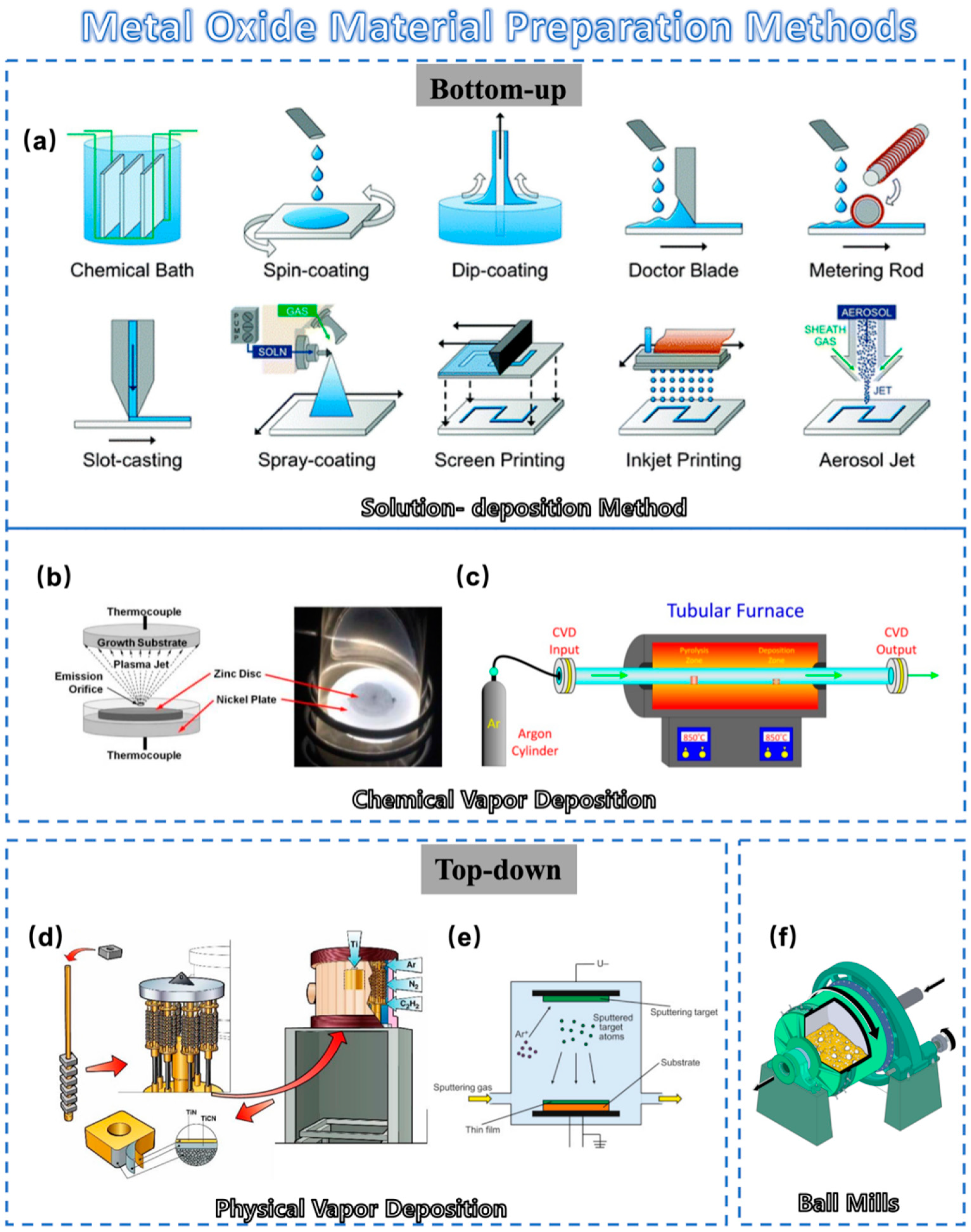
Figure 1. Schematic diagram of metal-oxide material preparation method: (a) Schematic of various solution-deposition processes: direct material growth without additional processing and liquid coating with additional processing to remove the solvent. (b) Schematic cross-section of a thermal plasma chemical vapor deposition (CVD) system used to deposit ZnO nanocrystal thin films. (c) A scheme showing the setup used to grow carbon nanotubes inside nanoporous anodic alumina templates by CVD. (d) Schematic diagram of conventional physical vapor deposition (PVD) process. (e) Schematic illustration of the PVD process. (f) A section cut-through of a ball mill.
2.1.2. Top-Down Approaches
-
Mechanical Milling: Mechanical milling is a very traditional and simple method of making metal-oxide powders. In this approach, metal-oxide powders are directly generated by mechanically grinding the bulk materials using a ball mill, as shown in Figure 1f. The electrical properties of metal oxides can easily be altered by adding other materials such as metals in this traditional method, as reported by Mikio et al. [27]. Using this method, Ag particles were added to NaxCo2O4 thermoelectric oxide. A mechanical milling process was included for uniform dispersion of Ag particles in the NaxCo2O4 matrix phase. Mechanical milling is also effective in reducing grain size, which is expected to affect the electrical resistivity and thermal conductivity of the product. However, it often lacks the capability of precise control over particle size distribution [27].
-
Physical Vapor Deposition: As one of the most common processes on the market (Figure 1d), PVD offers distinct advantages compared to other methods for preparing metal-oxide materials [28]. It excels in its precision at the micro- and nanoscale, resulting in high-quality, uniformly dense films (Figure 2e). Moreover, PVD operates at lower temperatures, reducing the risk of thermal stress [29]. PVD films are high-purity, environment-friendly, and compatible with most materials and substrates. These attributes render PVD highly sought after in electronic/optical coatings and material enhancement [30][31]. PVD methods for preparing metal-oxide materials encompass magnetron sputtering, laser deposition, ion beam deposition, molecular beam epitaxy, thermal evaporation, etc. These techniques play an important role in preparing metal-oxide films with desired structural properties [32][33][34][35][36][37].
2.2. The Advantages of Heterojunctions
2.2.1. Types of Heterojunctions
Researchers classify heterojunctions into all-organic heterojunctions, mixed organic–inorganic heterojunctions, and all-inorganic heterojunctions based on the type of material. All-organic heterojunctions usually have better processability and bendability [38], and substrate selection and growth techniques play a large role in achieving the desired material properties [39]. With high stability and high electron mobility, all-inorganic heterojunctions allow for device performance and are less flexible. These materials usually require high temperatures or complex preparation processes. Organic–inorganic hybrid heterojunctions combine the processability of organic materials with the high stability and high electron mobility of inorganic materials [40]. This structure allows for a better balance of electron and hole transport, improving the performance of electronic devices. However, the combination of such heterojunctions often requires a high degree of matching [41]. The choice of which heterojunction to use depends largely on the needs of the particular application, such as flexibility, stability, processing difficulty, and cost. Due to the presence of some micro/nano interactions such as surface and interface engineering, quantum confinement effects, strain engineering, chemical interactions, and doping [42][43][44][45][46], all kinds of heterojunctions have something in common; that is, the formation of heterojunctions allows the material properties to be improved dramatically, which is the basis of why heterojunctions involving metal oxides can be used in a wide range of applications, and this provides enlightenment for metal-oxide heterojunctions in neuromorphic applications.
2.2.2. Applications of Heterojunctions
Researchers have already introduced the superior properties of heterojunctions, and when metal-oxide materials are involved in heterojunctions, they often have their own unique advantages. Researchers will introduce the properties and applications of heterojunctions with the participation of metal oxides in some common areas.
-
Electrode materials for supercapacitors (SCs)
In recent years, transition-metal oxides (TMOs) have often been considered as the main cathode material for supercapacitors because of their versatile redox reactions, high theoretical capacitance, and economic feasibility [47][48]. However, TMOs always possess relatively low electrical conductivity, which leads to poor electrochemical performance, such as low specific capacitance, rate performance, and cycling stability [49].
Zhang et al. proposed a unique ZNCS/ZNCO heterostructure (Figure 2a) obtained by vulcanization of ZNCO for positive electrodes of SCs [50]. The resulting flower-like ZNCS/ZNCO composite exhibits several noteworthy advantages, including excellent conductivity, robust structural stability, and enhanced redox reactions. Therefore, the incorporation of oxide heterostructures has a positive impact on the performance of SCs.
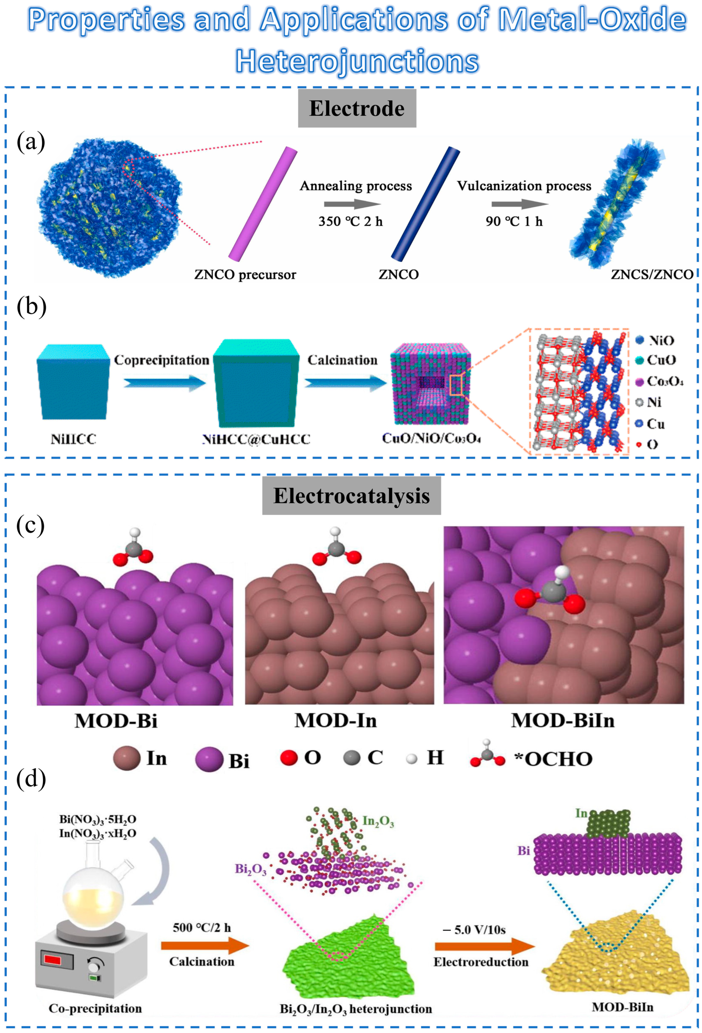
Figure 2. Schematic diagram of the preparation method for metal-oxide heterojunction and its applications: (a) Schematic formation process of ZNCS/ZNCO heterostructure composites. (b) Schematic diagram of the procedure for a hollow CuO/NiO/Co3O4 heterostructure. (c) The illustration of the fabrication process for Bi2O3/In2O3 heterojunction (MOD-BiIn) hybrid material. (d) The overview schematic of *OCHO on MOD-Bi, MOD-In, and MOD-BiIn surfaces.
In another work, Ju et al. proposed a ternary hollow CuO/ NiO/Co3O4 heterostructure (Figure 2b) [51]. Core–shell-structured Prussian blue analogs (PBAs) (NiHCC@CuHCC) with Ni-based PBAs (NiHCC) as the core and Cu-based PBAs (CuHCC) as the shell were prepared using the crystal seed method. The enhanced electrochemical performance could benefit from the following characteristics: (1) The hollow structure can provide more active sites, reduce the structural strain, and keep the electrode from collapsing. (2) The electronic structure of CuO/NiO heterojunction can be well tuned and finally facilitate the electron/ion migration [51].
In general, the synergetic effect between various metal oxides in a heterostructure facilitates electron/ion migration. More importantly, heterostructures often combine the advantages of all materials to achieve multiple advantages in various physical and chemical properties [51][52][53].
-
Excellent properties for electrocatalysis
The unique features of metal-oxide heterojunctions also confer substantial advantages in electrocatalytic applications.
Traditionally, catalysts with high CO2 reduction reaction (CO2RR) selectivity have relied on weak metal–hydrogen bonds to suppress hydrogen evolution reaction activity [54][55][56]. In recent years, materials derived from metal oxides or sulfides have been found to exhibit better electrocatalytic activity than their corresponding pure metal counterparts [57][58]. Specifically, Bi-based materials such as Bi-MOF, Bi2O3, or Bi2O2CO3 are commonly used as precursors for efficient electrocatalysts. However, these metal-oxide materials do not enhance the performance or maintain high selectivity [59]. However, indium-based metal-oxide heterojunctions can promote selectivity, especially when indium atoms are introduced at the metal sites of a heterojunction (Figure 2c) [60][61][62].
As shown in Figure 2d, Ye et al. synthesized a material containing partial bimetallic oxides (InxBi2-xO3) and heterojunctions (In2O3-Bi2O3) [59]. It was shown that heterojunctions can improve performance while maintaining high formate selectivity. This demonstrated that metal-oxide heterostructures have great potential for electrocatalysis. Furthermore, the role of heterojunctions can be also considered as an enlightening contribution in neuromorphic applications.
References
- Marjani, M.; Nasaruddin, F.; Gani, A.; Karim, A.; Hashem, I.A.T.; Siddiqa, A.; Yaqoob, I. Big IoT Data Analytics: Architecture, Opportunities, and Open Research Challenges. IEEE Access 2017, 5, 5247–5261.
- Gibney, E. Google AI Algorithm Masters Ancient Game of Go. Nature 2016, 529, 445–446.
- Yu, S. Neuro-Inspired Computing with Emerging Nonvolatile Memorys. Proc. IEEE 2018, 106, 260–285.
- Neumann, J. von First Draft of a Report on the EDVAC. IEEE Ann. Hist. Comput. 1993, 15, 27–75.
- Najafabadi, M.M.; Villanustre, F.; Khoshgoftaar, T.M.; Seliya, N.; Wald, R.; Muharemagic, E. Deep Learning Applications and Challenges in Big Data Analytics. J. Big Data 2015, 2, 1.
- Wu, Y.; Feng, J. Development and Application of Artificial Neural Network. Wirel. Pers. Commun. 2018, 102, 1645–1656.
- Moore, G.E. Cramming More Components onto Integrated Circuits, Reprinted from Electronics, Volume 38, Number 8, April 19, 1965, pp.114 ff. IEEE Solid-State Circuits Soc. Newsl. 2006, 11, 33–35.
- Kandel, E.R.; Koester, J.D.; Mack, S.H.; Siegelbaum, S.A. Principles of Neural Science, 6th ed.; McGraw Hill: New York, NY, USA, 2021.
- Oh, C.; Jo, M.; Son, J. All-Solid-State Synaptic Transistors with High-Temperature Stability Using Proton Pump Gating of Strongly Correlated Materials. ACS Appl. Mater. Interfaces 2019, 11, 15733–15740.
- He, Y.; Yang, Y.; Nie, S.; Liu, R.; Wan, Q. Electric-Double-Layer Transistors for Synaptic Devices and Neuromorphic Systems. J. Mater. Chem. C 2018, 6, 5336–5352.
- Merolla, P.A.; Arthur, J.V.; Alvarez-Icaza, R.; Cassidy, A.S.; Sawada, J.; Akopyan, F.; Jackson, B.L.; Imam, N.; Guo, C.; Nakamura, Y.; et al. A Million Spiking-Neuron Integrated Circuit with a Scalable Communication Network and Interface. Science 2014, 345, 668–673.
- Kim, Y.-H.; Heo, J.-S.; Kim, T.-H.; Park, S.; Yoon, M.-H.; Kim, J.; Oh, M.S.; Yi, G.-R.; Noh, Y.-Y.; Park, S.K. Flexible Metal-Oxide Devices Made by Room-Temperature Photochemical Activation of Sol–Gel Films. Nature 2012, 489, 128–132.
- Banger, K.K.; Yamashita, Y.; Mori, K.; Peterson, R.L.; Leedham, T.; Rickard, J.; Sirringhaus, H. Low-Temperature, High-Performance Solution-Processed Metal Oxide Thin-Film Transistors Formed by a ‘Sol–Gel on Chip’ Process. Nat. Mater. 2011, 10, 45–50.
- Yu, X.; Marks, T.J.; Facchetti, A. Metal Oxides for Optoelectronic Applications. Nat. Mater. 2016, 15, 383–396.
- Gai, L.-Y.; Lai, R.-P.; Dong, X.-H.; Wu, X.; Luan, Q.-T.; Wang, J.; Lin, H.-F.; Ding, W.-H.; Wu, G.-L.; Xie, W.-F. Recent Advances in Ethanol Gas Sensors Based on Metal Oxide Semiconductor Heterojunctions. Rare Met. 2022, 41, 1818–1842.
- Yao, Y.; Sang, D.; Duan, S.; Wang, Q.; Liu, C. Review on the Properties of Boron-Doped Diamond and One-Dimensional-Metal-Oxide Based P-N Heterojunction. Molecules 2021, 26, 71.
- Zhang, N.; Jiang, R. Interfacial Engineering of Metal/Metal Oxide Heterojunctions toward Oxygen Reduction and Evolution Reactions. ChemPlusChem 2021, 86, 1586–1601.
- Li, T.; Zeng, W.; Wang, Z. Quasi-One-Dimensional Metal-Oxide-Based Heterostructural Gas-Sensing Materials: A Review. Sens. Actuators B Chem. 2015, 221, 1570–1585.
- Pasquarelli, R.; Ginley, D.; O’Hayre, R. ChemInform Abstract: Solution Processing of Transparent Conductors: From Flask to Film. Chem. Soc. Rev. 2011, 40, 5406–5441.
- Liang, K.; Wang, R.; Huo, B.; Ren, H.; Li, D.; Wang, Y.; Tang, Y.; Chen, Y.; Song, C.; Li, F.; et al. Fully Printed Optoelectronic Synaptic Transistors Based on Quantum Dot–Metal Oxide Semiconductor Heterojunctions. ACS Nano 2022, 16, 8651–8661.
- Sakka, S.; Kozuka, H.; Zhao, G. Sol-Gel Preparation of Metal Particle/Oxide Nanocomposites. In Proceedings of the Sol-Gel Optics III; SPIE: Bellingham, WA, USA, 1994; Volume 2288, pp. 108–119.
- Ou, N.C.; Su, X.; Bock, D.C.; McElwee-White, L. Precursors for Chemical Vapor Deposition of Tungsten Oxide and Molybdenum Oxide. Coord. Chem. Rev. 2020, 421, 213459.
- Zhao, Q.; Zhao, D.; Zhao, J.; Fei, L. The Song Dynasty Shipwreck Monitoring and Analysis Using Acoustic Emission Technique. Forests 2019, 10, 767.
- Malandrino, G. Chemical Vapour Deposition. Precursors, Processes and Applications. Angew. Chem. Int. Ed. 2009, 48, 7478–7479.
- Yin, T.-H.; Liu, B.-J.; Lin, Y.-W.; Li, Y.-S.; Lai, C.-W.; Lan, Y.-P.; Choi, C.; Chang, H.-C.; Choi, Y. Electrodeposition of Copper Oxides as Cost-Effective Heterojunction Photoelectrode Materials for Solar Water Splitting. Coatings 2022, 12, 1839.
- Hu, R.; Liao, Y.; Qiao, H.; Li, J.; Wang, K.; Huang, Z.; Qi, X. Electrochemical Method Integrating Exfoliation and In-Situ Growth to Synthesize MoS2 Nanosheets/MnO2 Heterojunction for Performance-Enhanced Supercapacitor. Ceram. Int. 2022, 48, 23498–23503.
- Ito, M.; Furumoto, D. Effects of Mechanical Milling and Ag Addition on Thermoelectric Properties of NaxCo2O4. Scr. Mater. 2006, 55, 533–536.
- Reports, W.M. Physical Vapor Deposition Market Will Reach New Heights in the Upcoming Year 2022–2029. Oerlikon Balzers (Oerlikon Group), IHI Corporation, Silfex Inc. (Lam Research Corp.). Available online: https://www.openpr.com/news/2741878/physical-vapor-deposition-market-will-reach-new-heights-in (accessed on 27 October 2023).
- Campbell, S.A. The Science and Engineering of Microelectronic Fabrication; Oxford University Press: New York, NY, USA, 2001; ISBN 978-0-19-513605-0.
- O’Sullivan, J.; Burgess, S.; Rimmer, N. Metal Lift-off Using Physical Vapour Deposition. Microelectron. Eng. 2002, 64, 473–478.
- Radulescu, F.; Miller, P.; Cunnane, L.; Harris, M.; Lam, H.; Bowers, C. Complete Sputtering Metallization for High-Volume Manufacturing. III-Vs Rev. 2002, 15, 42–45.
- Wong, Y.H.; Cheong, K.Y. ZrO2 Thin Films on Si Substrate. J. Mater. Sci. Mater. Electron. 2010, 21, 980–993.
- Chin, W.C.; Cheong, K.Y.; Hassan, Z. Sm2O3 Gate Dielectric on Si Substrate. Mater. Sci. Semicond. Process. 2010, 13, 303–314.
- Nakazawa, H.; Sudoh, A.; Suemitsu, M.; Yasui, K.; Itoh, T.; Endoh, T.; Narita, Y.; Mashita, M. Mechanical and Tribological Properties of Boron, Nitrogen-Coincorporated Diamond-like Carbon Films Prepared by Reactive Radio-Frequency Magnetron Sputtering. Diam. Relat. Mater. 2010, 19, 503–506.
- Wasa, K.; Kitabatake, M.; Adachi, H. 4—Sputtering Systems. In Thin Film Materials Technology; Wasa, K., Kitabatake, M., Adachi, H., Eds.; William Andrew Publishing: Norwich, NY, USA, 2004; pp. 115–189. ISBN 978-0-8155-1483-1.
- Wasa, K.; Kitabatake, M.; Adachi, H. 5—Deposition of Compound Thin Films. In Thin Film Materials Technology; Wasa, K., Kitabatake, M., Adachi, H., Eds.; William Andrew Publishing: Norwich, NY, USA, 2004; pp. 191–403. ISBN 978-0-8155-1483-1.
- Wasa, K.; Kitabatake, M.; Adachi, H. 6—Structural Control of Compound Thin Films: Perovskite and Nanometer Oxide Thin Films. In Thin Film Materials Technology; Wasa, K., Kitabatake, M., Adachi, H., Eds.; William Andrew Publishing: Norwich, NY, USA, 2004; pp. 405–463. ISBN 978-0-8155-1483-1.
- Ni, Y.; Liu, L.; Liu, J.; Xu, W. A High-Strength Neuromuscular System That Implements Reflexes as Controlled by a Multiquadrant Artificial Efferent Nerve. ACS Nano 2022, 16, 20294–20304.
- Sassella, A.; Campione, M.; Raimondo, L.; Tavazzi, S.; Borghesi, A.; Goletti, C.; Bussetti, G.; Chiaradia, P. Epitaxial Growth of Organic Heterostructures: Morphology, Structure, and Growth Mode. Surf. Sci. 2007, 601, 2571–2575.
- Zhang, Y.; Gao, Y.; Carvalho, W.S.P.; Fang, C.; Serpe, M.J. Microgel-Based Stretchable Reservoir Devices for Elongation Enhanced Small Molecule Release Rate. ACS Appl. Mater. Interfaces 2020, 12, 19062–19068.
- Harhouz, A.; Hocini, A.; Tayoub, H. Ultracompact Gas-Sensor Based on a 2D Photonic Crystal Waveguide Incorporating with Tapered Microcavity. IOP Conf. Ser. Mater. Sci. Eng. 2021, 1046, 012001.
- Liu, Z.; Li, M.; Sun, Y.; Wang, H.; Chen, H.; Tian, Y.; Wang, H.; Ding, Y.; Chen, Z. Integrating Surface and Interface Engineering to Improve Optoelectronic Performance and Environmental Stability of MXene-Based Heterojunction towards Broadband Photodetection. Nano Res. 2023, 16, 10148–10155.
- Shen, R.; Jiang, C.; Xiang, Q.; Xie, J.; Li, X. Surface and Interface Engineering of Hierarchical Photocatalysts. Appl. Surf. Sci. 2019, 471, 43–87.
- Koretomo, D.; Hamada, S.; Magari, Y.; Furuta, M. Quantum Confinement Effect in Amorphous In–Ga–Zn–O Heterojunction Channels for Thin-Film Transistors. Materials 2020, 13, 1935.
- Shi, J.; Starr, M.B.; Wang, X. Band Structure Engineering at Heterojunction Interfaces via the Piezotronic Effect. Adv. Mater. 2012, 24, 4683–4691.
- Lu, L.; Xu, T.; Chen, W.; Lee, J.M.; Luo, Z.; Jung, I.H.; Park, H.I.; Kim, S.O.; Yu, L. The Role of N-Doped Multiwall Carbon Nanotubes in Achieving Highly Efficient Polymer Bulk Heterojunction Solar Cells. Nano Lett. 2013, 13, 2365–2369.
- Lemmermann, T.; Becker, M.; Stehle, M.; Drache, M.; Beuermann, S.; Bogar, M.S.; Gohs, U.; Fittschen, U.E.A.; Turek, T.; Kunz, U. In Situ and in Operando Detection of Redox Reactions with Integrated Potential Probes during Vanadium Transport in Ion Exchange Membranes. J. Power Source 2022, 533, 231343.
- Ge, Y.; Liu, Z.; Wu, Y.; Holze, R. On the Utilization of Supercapacitor Electrode Materials. Electrochim. Acta 2021, 366, 137390.
- Lu, W.; Shen, J.; Zhang, P.; Zhong, Y.; Hu, Y.; Lou, X.W. Construction of CoO/Co-Cu-S Hierarchical Tubular Heterostructures for Hybrid Supercapacitors. Angew. Chem. 2019, 131, 15587–15593.
- Zhang, Y.; Huang, L.; Lei, X.; Huang, H.; Guo, W.; Wang, S. Hierarchical Ternary Zn-Ni-Co Sulfide/Oxide Heterostructure for High Specific Energy Hybrid Supercapacitor. J. Alloys Compd. 2023, 962, 171201.
- Ju, H.; Tang, Q.; Xu, Y.; Bai, X.; Pu, C.; Liu, T.; Liu, S.; Zhang, L. Prussian Blue Analogue-Derived Hollow Metal Oxide Heterostructure for High-Performance Supercapacitors. Dalton Trans. 2023, 52, 12948–12957.
- Rajak, R.; Saraf, M.; Mobin, S.M. Robust Heterostructures of a Bimetallic Sodium–Zinc Metal–Organic Framework and Reduced Graphene Oxide for High-Performance Supercapacitors. J. Mater. Chem. A 2019, 7, 1725–1736.
- Zhang, Y.; Li, L.; Su, H.; Huang, W.; Dong, X. Binary Metal Oxide: Advanced Energy Storage Materials in Supercapacitors. J. Mater. Chem. A 2015, 3, 43–59.
- Jia, J.; Hao, X.; Chang, Y.; Jia, M.; Wen, Z. Rational Design of Cu3PdN Nanocrystals for Selective Electroreduction of Carbon Dioxide to Formic Acid. J. Colloid Interface Sci. 2021, 586, 491–497.
- Zhu, W.; Zhao, K.; Liu, S.; Liu, M.; Peng, F.; An, P.; Qin, B.; Zhou, H.; Li, H.; He, Z. Low-Overpotential Selective Reduction of CO2 to Ethanol on Electrodeposited CuxAuy Nanowire Arrays. J. Energy Chem. 2019, 37, 176–182.
- Dai, W.; Long, J.; Yang, L.; Zhang, S.; Xu, Y.; Luo, X.; Zou, J.; Luo, S. Oxygen Migration Triggering Molybdenum Exposure in Oxygen Vacancy-Rich Ultra-Thin Bi2MoO6 Nanoflakes: Dual Binding Sites Governing Selective CO2 Reduction into Liquid Hydrocarbons. J. Energy Chem. 2021, 61, 281–289.
- Wang, S.; Kou, T.; Baker, S.E.; Duoss, E.B.; Li, Y. Recent Progress in Electrochemical Reduction of CO2 by Oxide-Derived Copper Catalysts. Mater. Today Nano 2020, 12, 100096.
- Li, F.; Chen, L.; Xue, M.; Williams, T.; Zhang, Y.; MacFarlane, D.R.; Zhang, J. Towards a Better Sn: Efficient Electrocatalytic Reduction of CO2 to Formate by Sn/SnS2 Derived from SnS2 Nanosheets. Nano Energy 2017, 31, 270–277.
- Ye, R.; Zhu, J.; Tong, Y.; Feng, D.; Chen, P. Metal Oxides Heterojunction Derived Bi-In Hybrid Electrocatalyst for Robust Electroreduction of CO2 to Formate. J. Energy Chem. 2023, 83, 180–188.
- Tan, D.; Lee, W.; Kim, Y.E.; Ko, Y.N.; Youn, M.H.; Jeon, Y.E.; Hong, J.; Park, J.E.; Seo, J.; Jeong, S.K.; et al. In–Bi Electrocatalyst for the Reduction of CO2 to Formate in a Wide Potential Window. ACS Appl. Mater. Interfaces 2022, 14, 28890–28899.
- Wu, M.; Xiong, Y.; Hu, B.; Zhang, Z.; Wei, B.; Li, L.; Hao, J.; Shi, W. Indium Doped Bismuth Subcarbonate Nanosheets for Efficient Electrochemical Reduction of Carbon Dioxide to Formate in a Wide Potential Window. J. Colloid Interface Sci. 2022, 624, 261–269.
- Wang, Q.; Yang, X.; Zang, H.; Chen, F.; Wang, C.; Yu, N.; Geng, B. Metal–Organic Framework-Derived BiIn Bimetallic Oxide Nanoparticles Embedded in Carbon Networks for Efficient Electrochemical Reduction of CO2 to Formate. Inorg. Chem. 2022, 61, 12003–12011.
More
Information
Subjects:
Engineering, Electrical & Electronic
Contributors
MDPI registered users' name will be linked to their SciProfiles pages. To register with us, please refer to https://encyclopedia.pub/register
:
View Times:
781
Revisions:
2 times
(View History)
Update Date:
28 Dec 2023
Table of Contents


Notice
You are not a member of the advisory board for this topic. If you want to update advisory board member profile, please contact office@encyclopedia.pub.
OK
Confirm
Only members of the Encyclopedia advisory board for this topic are allowed to note entries. Would you like to become an advisory board member of the Encyclopedia?
Yes
No
${ textCharacter }/${ maxCharacter }
Submit
Cancel
Back
Comments
${ item }
|
${ item.createdUser.fullName }
${ item.createdAt }
${ item.vote }
${ item.reply }
Delete
${ reply.createdUser.fullName }
${ reply.createdAt }
${ reply.vote }
Delete
There is no reply to this comment~
${ item.replyTextCharacter }/${ item.replyMaxCharacter }
Submit
Cancel
More
No more~
There is no comment~
${ textCharacter }/${ maxCharacter }
Submit
Cancel
${ selectedItem.replyTextCharacter }/${ selectedItem.replyMaxCharacter }
Submit
Cancel
Confirm
Are you sure to Delete?
Yes
No