Your browser does not fully support modern features. Please upgrade for a smoother experience.
Please note this is a comparison between Version 1 by Jie Jiang and Version 2 by Rita Xu.
As technologies like the Internet, artificial intelligence, and big data evolve at a rapid pace, computer architecture is transitioning from compute-intensive to memory-intensive. The emulation of the behaviors of a synapse at the device level by ionic/electronic devices has shown promising potential in future neural-inspired and compact artificial intelligence systems.
- metal oxide
- heterojunction
- memristor
- transistor
1. Introduction
Since the invention of the computer, technological progress has led to continuous improvements in computer performance and device function. Especially in recent years, the rapid technological developments for the Internet of Things and artificial intelligence (AI) have significantly increased the requirements for computer data processing [1][2][3][1,2,3]. Traditional von Neumann architectures could successfully solve the structural problem [4], but they encounter substantial challenges in contemporary computing, which are named the von Neumann bottleneck. At present, there are growing developments of new algorithms, such as artificial neural networks and deep learning [5][6][5,6]. Meanwhile, since the complementary metal-oxide semiconductor (CMOS) transistor may have reached its limit in terms of size, Moore’s law may begin to break down [7]. In contrast, the human brain, with a high parallelism, has a low power of 20 W because the average synaptic power consumption is only about 10 fJ [8][9][10][8,9,10]. Therefore, brain-inspired neuromorphic devices have attracted increasing interest as a potential solution for breaking the von Neumann bottleneck [11].
At the same time, metal-oxide materials may provide an ideal platform for the development of multifunctional neuromorphic devices due to their low power consumption, high stability, versatility, low cost, etc. [12][13][14][12,13,14]. Moreover, as basic building blocks, metal-oxide heterojunctions have an intriguing performance due to their higher charge mobility, lower leakage current, and faster response time ascribed to interfacial states and band bending [15][16][17][18][15,16,17,18]. Such heterojunctions allow the combination of different types of metal oxides to achieve more functionalities and better performances. Therefore, neuromorphic devices based on metal-oxide heterojunctions may provide a great opportunity for next-generation computing technologies.
2. Metal-Oxide Heterojunction
2.1. Preparation of Metal-Oxide Materials
The synthesis and preparation of metal-oxide materials can be classified into two main categories: bottom-up and top-down approaches.2.1.1. Bottom-Up Approaches
-
Solution-Deposition Method: Solution-deposition methods include a variety of methods (Figure 1a). Solution techniques allow for the deposition of films at atmospheric pressure with minimal equipment cost. Scalable deposition methods that allow for uniform, large-area coverage are important for high-throughput industrial applications [19][22]. ResearchWers highlight the sol–gel method and inkjet printing method in this section. The latter method mainly involves transforming the desired precursor material into an inkjet state and then distributing it for printing in the same way as other solution-deposition methods. A new kind of fully inkjet-printed InP/ZnSe QD/SnO2 heterostructure thin film transistor (TFT) was fabricated with a bottom-gate, top-contact configuration by Liang et al. [20][27]. The fully printed device on a glass substrate exhibited a high optical transparency in the visible spectrum. This chemical method allows the formation of metal oxides using a colloidal solution (sol) approach. This method can well control composition and structure at the nanoscale. However, this process is always slow and often requires post-synthesis calcination [21][28].
-
Chemical Vapor Deposition: Chemical vapor deposition is a process in which the substrate is exposed to one or more volatile precursors, and then reaction and decomposition are performed on the substrate surface to create the desired thin film. In typical CVD (Figure 1b), precursor gases are fed into the reaction chamber at ambient temperature. When they pass or come in contact with the heated substrate, they react or decompose to form a solid phase and then are deposited on the substrate. As shown in Figure 1c, the substrate temperature is very important and can affect the reactions that will take place. Compared to sol–gel methods, it typically offers a high degree of compositional and crystal structure control for precise material design. As a result, CVD has attracted growing interest in the semiconductor industry due to its large-area growth ability [22][23][24][29,30,31].
-
Electrodeposition: Electrodeposition is a method for depositing ions from a solution onto an electrode’s surface through an electrochemical reaction [25][32]. For example, Yin et al. easily prepared Cu2O thin films using the electrodeposition method, thereby creating P-type Cu-based metal-oxide materials with excellent photoelectrochemical water splitting capability [25][32]. Unlike CVD, electrodeposition typically does not require high-temperature treatment or hazardous gases, making it environment-friendly. Moreover, it is a cost-effective way as it does not necessitate high-vacuum equipment or expensive precursors. These advantages make it an emerging favorite for the electronic materials [25][26][32,33].
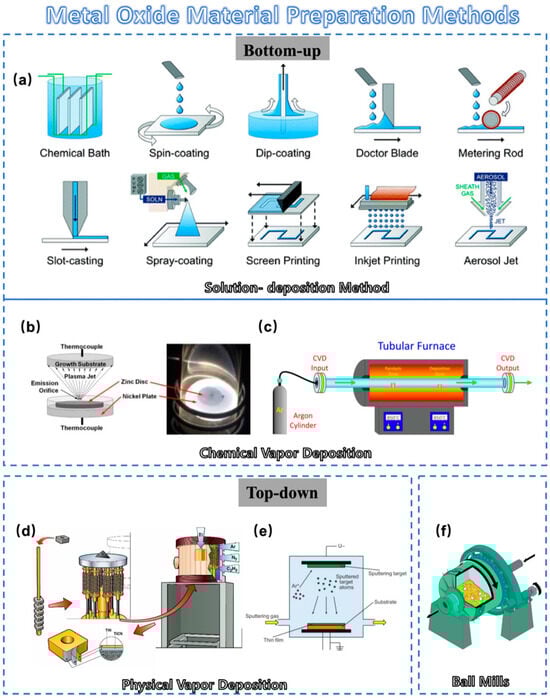
Figure 1. Schematic diagram of metal-oxide material preparation method: (a) Schematic of various solution-deposition processes: direct material growth without additional processing and liquid coating with additional processing to remove the solvent. (b) Schematic cross-section of a thermal plasma chemical vapor deposition (CVD) system used to deposit ZnO nanocrystal thin films. (c) A scheme showing the setup used to grow carbon nanotubes inside nanoporous anodic alumina templates by CVD. (d) Schematic diagram of conventional physical vapor deposition (PVD) process. (e) Schematic illustration of the PVD process. (f) A section cut-through of a ball mill.
2.1.2. Top-Down Approaches
-
Mechanical Milling: Mechanical milling is a very traditional and simple method of making metal-oxide powders. In this approach, metal-oxide powders are directly generated by mechanically grinding the bulk materials using a ball mill, as shown in Figure 1f. The electrical properties of metal oxides can easily be altered by adding other materials such as metals in this traditional method, as reported by Mikio et al. [27][38]. Using this method, Ag particles were added to NaxCo2O4 thermoelectric oxide. A mechanical milling process was included for uniform dispersion of Ag particles in the NaxCo2O4 matrix phase. Mechanical milling is also effective in reducing grain size, which is expected to affect the electrical resistivity and thermal conductivity of the product. However, it often lacks the capability of precise control over particle size distribution [27][38].
-
Physical Vapor Deposition: As one of the most common processes on the market (Figure 1d), PVD offers distinct advantages compared to other methods for preparing metal-oxide materials [28][36]. It excels in its precision at the micro- and nanoscale, resulting in high-quality, uniformly dense films (Figure 2e). Moreover, PVD operates at lower temperatures, reducing the risk of thermal stress [29][39]. PVD films are high-purity, environment-friendly, and compatible with most materials and substrates. These attributes render PVD highly sought after in electronic/optical coatings and material enhancement [30][31][40,41]. PVD methods for preparing metal-oxide materials encompass magnetron sputtering, laser deposition, ion beam deposition, molecular beam epitaxy, thermal evaporation, etc. These techniques play an important role in preparing metal-oxide films with desired structural properties [32][33],43[34],44[35][36],45[37][42,46,47].
2.2. The Advantages of Heterojunctions
2.2.1. Types of Heterojunctions
RWesearchers classify heterojunctions into all-organic heterojunctions, mixed organic–inorganic heterojunctions, and all-inorganic heterojunctions based on the type of material. All-organic heterojunctions usually have better processability and bendability [38][48], and substrate selection and growth techniques play a large role in achieving the desired material properties [39][49]. With high stability and high electron mobility, all-inorganic heterojunctions allow for device performance and are less flexible. These materials usually require high temperatures or complex preparation processes. Organic–inorganic hybrid heterojunctions combine the processability of organic materials with the high stability and high electron mobility of inorganic materials [40][50]. This structure allows for a better balance of electron and hole transport, improving the performance of electronic devices. However, the combination of such heterojunctions often requires a high degree of matching [41][51]. The choice of which heterojunction to use depends largely on the needs of the particular application, such as flexibility, stability, processing difficulty, and cost. Due to the presence of some micro/nano interactions such as surface and interface engineering, quantum confinement effects, strain engineering, chemical interactions, and doping [42][43][44][45][46][52,53,54,55,56], all kinds of heterojunctions have something in common; that is, the formation of heterojunctions allows the material properties to be improved dramatically, which is the basis of why heterojunctions involving metal oxides can be used in a wide range of applications, and this provides enlightenment for metal-oxide heterojunctions in neuromorphic applications.2.2.2. Applications of Heterojunctions
ResWearchers have already introduced the superior properties of heterojunctions, and when metal-oxide materials are involved in heterojunctions, they often have their own unique advantages. ResearchersWe will introduce the properties and applications of heterojunctions with the participation of metal oxides in some common areas.-
Electrode materials for supercapacitors (SCs)
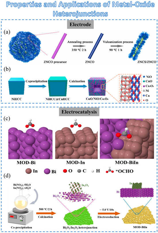
Figure 2. Schematic diagram of the preparation method for metal-oxide heterojunction and its applications: (a) Schematic formation process of ZNCS/ZNCO heterostructure composites. (b) Schematic diagram of the procedure for a hollow CuO/NiO/Co3O4 heterostructure. (c) The illustration of the fabrication process for Bi2O3/In2O3 heterojunction (MOD-BiIn) hybrid material. (d) The overview schematic of *OCHO on MOD-Bi, MOD-In, and MOD-BiIn surfaces.
-
Excellent properties for electrocatalysis