Your browser does not fully support modern features. Please upgrade for a smoother experience.
Submitted Successfully!
 +1 credit
Thank you for your contribution! You can also upload a video entry or images related to this topic.
For video creation, please contact our Academic Video Service.
| Version | Summary | Created by | Modification | Content Size | Created at | Operation |
|---|---|---|---|---|---|---|
| 1 | Stefano Stassi | -- | 6072 | 2023-12-22 14:40:58 | | | |
| 2 | Jason Zhu | -4 word(s) | 6068 | 2023-12-25 02:53:53 | | | | |
| 3 | Jason Zhu | + 13 word(s) | 6081 | 2023-12-29 03:56:32 | | |
Video Upload Options
We provide professional Academic Video Service to translate complex research into visually appealing presentations. Would you like to try it?
Cite
If you have any further questions, please contact Encyclopedia Editorial Office.
Arduino, D.; Stassi, S.; Spano, C.; Scaltrito, L.; Ferrero, S.; Bertana, V. Silicon and Silicon Carbide Recrystallization by Laser Annealing. Encyclopedia. Available online: https://encyclopedia.pub/entry/53072 (accessed on 25 July 2026).
Arduino D, Stassi S, Spano C, Scaltrito L, Ferrero S, Bertana V. Silicon and Silicon Carbide Recrystallization by Laser Annealing. Encyclopedia. Available at: https://encyclopedia.pub/entry/53072. Accessed July 25, 2026.
Arduino, Daniele, Stefano Stassi, Chiara Spano, Luciano Scaltrito, Sergio Ferrero, Valentina Bertana. "Silicon and Silicon Carbide Recrystallization by Laser Annealing" Encyclopedia, https://encyclopedia.pub/entry/53072 (accessed July 25, 2026).
Arduino, D., Stassi, S., Spano, C., Scaltrito, L., Ferrero, S., & Bertana, V. (2023, December 22). Silicon and Silicon Carbide Recrystallization by Laser Annealing. In Encyclopedia. https://encyclopedia.pub/entry/53072
Arduino, Daniele, et al. "Silicon and Silicon Carbide Recrystallization by Laser Annealing." Encyclopedia. Web. 22 December, 2023.
Copy Citation
Modifying material properties within a specific spatial region is a pivotal stage in the fabrication of microelectronic devices. Laser annealing emerges as a compelling technology, offering precise control over the crystalline structure of semiconductor materials and facilitating the activation of doping ions in localized regions. This obviates the necessity for annealing the entire wafer or device.
laser annealing
silicon
silicon carbide
crystallization
integrated devices
1. Introduction
The rapid diffusion of microelectronics and their advancement toward improved performance and reduced size has necessitated the development of new technological processes for selectively modifying material properties in specific regions without affecting others. For instance, there is a need to locally crystallize amorphous materials to achieve new properties or activate dopant ions that have been previously implanted in a semiconductor region. This can be accomplished through semiconductor annealing. Traditional annealing methods involve heating samples to high temperatures (above 1000 °C) using furnaces to repair lattice damage and electrically activate dopants.
Thermal annealing is a critical step in semiconductor device fabrication that is typically performed after other processes. Subjecting the entire sample to high temperatures can have undesirable side effects on device functionality, including impurity redistribution and damage to implanted ion disposition [1]. Moreover, it is incompatible with prior metal deposition, as the elevated temperature can cause metal connections to melt and redistribute.
In recent years, various alternatives to thermal annealing in furnaces have been explored, with laser annealing emerging as one of the most effective technologies [2]. Depending on the light frequency, laser annealing offers the advantage of intense absorption on a thin surface layer (a few nanometers deep). This capability allows for the generation of the extremely high temperatures necessary for annealing lattice damage or crystallizing amorphous films in a precisely localized region. Importantly, this occurs without affecting the rest of the sample, mitigating the risk of unwanted alterations to the device [3].
During the laser annealing process, the material phase (crystallinity), optical properties (refractive index, light absorption), and electrical properties (conductivity, energy bandgap, direct or indirect bandgap) of the samples are altered through light absorption [4]. The incident laser energy is absorbed through electronic excitations and rapidly transferred to the lattice, resulting in the melting of the crystal to a certain depth and inducing lattice damage. Subsequently, liquid phase epitaxial regrowth occurs from the undamaged substrate underneath, leading to recrystallization of the melted region into nearly perfect single-crystal material, with dopants occupying substitutional sites in the lattice, thereby activating the implanted ions [5].
Laser annealing is a versatile technique applicable to various types of semiconductors, including group IV semiconductors like silicon, germanium [6], and silicon carbide, as well as III-V compound semiconductors like gallium arsenide [7][8].
Laser thermal annealing is an ultrafast and low thermal budget process solution for the passivation of backside illuminated sensors and power devices. Laser annealing can be a solution for the backside contact of those chips with a vertical flow of electrical current, where an ohmic contact and/or collector on the wafer backside are required [9][10], including SiC power Metal-Oxide-Semiconductor Field Effect Transistors (MOSFET) [11], Insulated Gate Bipolar Transistor (IGBT) [12], and high voltage diodes [13][14]. Moreover, this process can also be useful for the ohmic contact formation process in SiC Schottky diodes, causing a negligible impact on the device’s front side [15][16]. The laser annealing process has also been used to activate doping ions in the source and drain region of MOSFET to avoid damage to the channel region induced by global device heating processes such as rapid thermal annealing (RTA) [17][18][19]. A scheme of laser annealing processes in semiconductor devices is reported in Figure 1. The high-temperature annealing region is restricted to thin layers while keeping underlying layers at low temperatures. An ultrafast annealing time and proper laser parameters may achieve high performance and high yields, locking in the surface properties without damaging buried device layers [20].
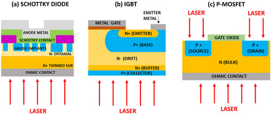
Figure 1. Scheme of the laser annealing process exploited to (a) form ohmic contact on the Schottky diode, (b) activate doping on the collector layer of IGBT, and (c) activate doping in the source and drain region and form ohmic contact in a MOSFET (in this case a pMOSFET, although the process is the same for nMOSFET).
2. Laser Annealing Theory
Laser annealing is a technique that involves using light absorption to deliver energy to a material. Typically, laser annealing is limited to thin surface layers because the intensity of the incident light decreases as it penetrates the material, based on the material’s absorption coefficient, α. The Beer–Lambert law describes this decay of intensity with depth z using the equation:
where I0 is the intensity on the surface.
The optical penetration or absorption depth, defined as the depth at which the transmitted light’s intensity drops to 1/e (about 37%) of its initial value on the surface, is denoted as δ = 1/α. Both α and δ depend on the semiconductor type, laser wavelength, and temperature.
Since energy absorption is primarily confined to the absorption depth, this parameter is applicable to all beam profiles, even though it was originally developed for plane waves. Consequently, it is possible to locally modify surface properties without altering the bulk material by using laser wavelengths with short absorption depths [21].
In continuous wave (CW) or nanosecond laser pulses, it is generally assumed that single-photon interactions account for most of the absorption. However, in the case of picosecond (ps) and femtosecond (fs) lasers, the absorption depths can be reduced due to phenomena such as optical breakdown and multiphoton absorption, which result from the extremely high instantaneous intensity of these lasers [22].
The absorption of laser light in insulators and semiconductors is typically achieved through resonant excitations, such as transitions of valence band electrons to the conduction band (interband transitions, Figure 2) or within bands (intersubband transitions) [23].
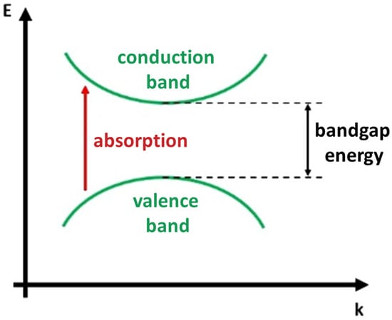
Figure 2. Scheme of the material interband photon absorption.
Typically, photons interact with the electronic or vibrational states present in a material based on their energy. Laser photons of energy greater than that of the band gap generate electron-hole pairs promoted to states of higher kinetic energy in the conduction and valence band. These excited electronic states can subsequently transfer energy to lattice phonons, becoming heat. If there are no other factors such as impurity or defect states or multiphoton absorption, photons with energy lower than the material’s band gap will not be absorbed. This generally corresponds to light wavelengths within the infrared to visible spectrum for semiconductors and within the vacuum ultraviolet range (below 200 nm) for insulators.
The laser field to the electronic system is quickly transferred to phonons in less than 1 picosecond, leading to the melting of the near-surface region [24]. The near-surface region of a sample can melt and stay molten for a thermalization time depending on the material treated, during which dopant diffusion in the liquid state and nonequilibrium segregation occur together with ultrarapid recrystallization [25]. The crystallization process can be described in terms of models based on macroscopic diffusion equations for heat and mass transport. The mechanism can be explained in terms of a molten layer that extends all over the amorphous thickness and whose subsequent solidification occurs on a crystalline seed, like a liquid phase epitaxy [24]. In this way, the laser treatment allows the annealing and treatment of the lattice damage caused by ion implantation, diffuse surface-deposited dopant films, and recrystallized doped amorphous films deposited on the substrate [25].
The specific material and its mechanisms determine the time required for excited electronic states to transfer energy to phonons and thermalize. For non-metals, the thermalization time can be from 10−8 s to 10−6 s, while it is around 10−12–10−10 s for metals [22]. If the laser-induced excitation rate is lower than the thermalization rate, the transient electronically excited states are not significant and the absorbed laser energy can be considered directly converted into heat. This process is known as photothermal (pyrolytic) processing and is commonly observed in semiconductor laser processing with long pulse times (>ns). During this process, material response can be analyzed purely in thermal terms [21].
However, when the laser-induced excitation rate exceeds the thermalization rate, significant excitations can accumulate in the intermediate states. This can lead to direct bond-breaking due to the excitation energies, resulting in non-thermal material modifications. This phenomenon is referred to as photochemical (photolytic) processing, where there are no changes in the system’s temperature. Ultrafast femtosecond laser pulses with short-wavelength light, where the photon energy is comparable to the chemical bond energy, can trigger photochemical processing [26].
The laser annealing process is significantly influenced by the technology of the implemented system, which determines the wavelength and the shortest pulse duration of the laser. Several key parameters of the laser system can be adjusted to control the effects of the annealing process on the material surface. A list of the most crucial system specifications and parameters involved in laser annealing processes is provided below. These descriptions aim to enhance understanding of the main results in silicon and silicon carbide annealing processes described in the following sections.
Laser technology: The laser relies on a certain physical mechanism depending on the laser material, which affects the other laser parameters (such as its power, pulse duration, etc.). Possible laser technologies range from gas lasers (such as CO2 laser) to excimer lasers (based on a combination of a noble gas and a reactive gas, such as KrF and XeCl lasers) and solid-state lasers (based on doped crystal, such as Nd:YAG lasers).
Wavelength: This parameter plays a significant role in the annealing process as it affects light absorption efficiency and the depth of laser effects in the material. Generally, the penetration depth is proportional to λ/4πk with k, which is the absorption coefficient. The light wavelength (which is directly related to photon energy by the Planck equation) must fit with the material bandgap to be absorbed, otherwise, photons pass through the material. Laser wavelengths used for annealing range from infrared to visible and ultraviolet (UV) regions.
Power and spot size: A combination of these two parameters defines the power density, which indicates the energy quantity delivered by the laser beam to the desired target per unit of area and time. The energy density or fluence represents the energy transferred per unit area by a single pulse. The use of a magnifying lens can increase the given number of photons directed to a specific area, raising the laser fluence and thus the target temperature faster.
Pulse duration. This is the time between the beginning and end edges of an energy pulse, often measured at full-width half maximum (FWHM). Lasers treated in this review are characterized by nanosecond or femtosecond pulses. Generally, considering a fixed frequency, short pulses allow samples to cool down between bursts of light and, hence protect illuminated samples from overheating. However, in general, short pulses with high peak powers (as in the case of femtosecond lasers) may ablate the surface material, avoiding heating the surrounding area. Obviously, this parameter is absent in the case of continuous wave lasers.
Scanning speed: This parameter represents the velocity of the relative motion between the laser and the material. Slower scanning speeds result in the laser remaining in a particular spatial position on the material for a longer time, leading to higher annealing effects.
Beam profile: The laser beam can have various profiles, such as Gaussian, multimode, or rectangular. The energy distribution of the beam determines the spatial effect of the annealing process, yielding different results. Gaussian beams, for example, cause stronger effects near the beam center and weaker effects near the edges, while rectangular beams provide a more uniform spatial distribution.
Environment: Since laser annealing increases the local temperature of the material, environmental conditions can impact process outcomes. The presence of air can cause reactions between the heated material and atmospheric gases, which is not observed in a vacuum or an argon (Ar) atmosphere.
Manipulating these main parameters is possible by taking advantage of the main components of the laser annealing equipment, which consists of a laser source composed of a laser head (which determines the emitted wavelength, frequency, and pulse duration), lenses, and filters for shaping the laser beam profile.
A laser stage motor is normally responsible for the scan speed. Indeed, the laser head can be based on the technology called plotter laser, where the laser light is driven by some fixed internal mirrors, and its movement on the sample surface is controlled by a stage motor that determines the scan speed and the resolution on the X and Y axes. An alternative technology is the galvo head, where the laser ray is driven by rotating dynamic internal mirrors, and a stage motor is used only for large displacement.
3. Silicon Laser Annealing
Silicon is a crucial material for creating microelectronic devices, and various fabrication processes have been developed to manipulate its properties based on specific applications. One important technique being studied is its transformation from amorphous silicon to polycrystalline silicon, which combines the advantages of both single-crystal silicon and amorphous silicon [27]. While amorphous silicon has lower carrier mobility, it is cost-effective to manufacture. On the other hand, polycrystalline silicon, though inferior in mechanical and electrical properties compared to single-crystal silicon, finds extensive use in the field of optoelectronics.
Currently, laser annealing is the most commonly employed technology for preparing polysilicon materials. This method involves the use of a high-power pulsed laser on an amorphous silicon sample. The surface of the amorphous silicon absorbs the laser energy, causing the temperature to rise to the phase transition point. After cooling and solidification, the amorphous silicon is transformed into polysilicon [28][29].
This process exhibits short annealing time and high crystallization efficiency. Additionally, laser annealing keeps the substrate at a low temperature, reducing the requirements on the substrate material and thus lowering manufacturing costs.
The crystallization of silicon grains is influenced by energy density, pulse duration, and laser shape; however, laser wavelength is the primary parameter governing the crystallization phenomenon due to its role in optical absorption [30].
Specifically, crystallization occurs when the photon energy (associated with the photon wavelength) matches the bandgap of the material. The light induces a transition between the ground and excited states, resulting in the loss of a photon and the production of an excited state [31]. In the case of silicon, which has a bandgap energy of 1.1 eV, the minimum wavelength required for electron transition from the valence to the conduction band is around 1100 nm, corresponding to the infrared (IR) region.
Several experiments have been conducted on silicon laser annealing using IR laser sources. Salman et al. [32] successfully crystallized a silicon sample using an IR-pulsed laser with a wavelength of 1064 nm (photon energy of 1.165 eV) and a pulse duration of 200 ns. The experiment was performed under ambient conditions using a pulsed fiber laser built on Ytterbium-doped active fiber, with an average optical power of 20 W and a maximum pulse energy of 0.50 mJ. The repetition rate was set to 20 kHz. Successful crystallization was confirmed through Raman spectroscopy analysis, showing a main scattering peak at 520 cm−1, which is typical of a crystalline silicon structure. The crystallization process was also verified using Fourier Transform Infrared (FTIR) spectroscopy, Scanning Electron Microscopy (SEM), Transmission Electron Microscopy (TEM), and Atomic Force Microscopy (AFM), which are powerful analysis tools for investigating semiconductor crystalline structures.
Previous studies [33][34] have utilized infrared laser radiation with a wavelength of 800 nm, generated by a Ti:Sapphire laser system with femtosecond pulse duration. Despite this difference, the presence of crystalline grains can be observed from AFM, SEM, and TEM measurements, indicating the successful attainment of polysilicon through the annealing process.
Other groups [35][36] have demonstrated the effectiveness of IR radiation (λ = 800 nm by Zhan et al. [35] and λ = 1026 nm by Bronnikov et al. [36]) for silicon crystallization using laser systems based on different technologies (Yb:KGW laser system). Before the laser annealing process, the Raman spectra of the as-grown amorphous film display a broad peak, ranging from 420 to 530 cm−1, associated with the optical vibration modes of amorphous silicon [37][38]. However, after the annealing step, a distinct crystalline peak at 513 cm−1 becomes evident. The sharp peak exhibits a blue shift of approximately 7 cm−1 compared to the peak of single crystalline silicon due to phonon confinement in nanocrystalline silicon and mechanical stress induced in the lattice by femtosecond laser treatment [37].
Laser annealing experiments have also explored more energetic wavelengths in the near UV range (200–400 nm) [39] and visible range (400–780 nm) [40][41]. For instance, Pan et al. utilized near ultraviolet (λ ≈ 400 nm) femtosecond laser annealing in a scanning mode to crystallize amorphous silicon (a-Si) films at room temperature. They investigated the impact of laser fluence, beam overlap, and number of laser shots on the average grain size of the resulting polycrystalline silicon. The experiment revealed that increasing either the beam overlap at a fixed fluence or the fluence for a fixed number of shots generally leads to larger grain sizes [42]. Additionally, they compared the crystallization degree of the polysilicon obtained through UV annealing with that produced by IR annealing (λ ≈ 800 nm) using Raman spectroscopy.
In contrast, cross-sectional SEM images showed that the 100 nm thick a-Si film is not fully crystallized by UV annealing, unlike in the case of IR annealing. This can be attributed to the much shorter penetration depth of 400 nm light in amorphous silicon compared to 800 nm light.
UV radiation with nanosecond pulse durations has also been tested [43][44][45][46], as demonstrated by Garcia et al. [30]. They employed solid-state laser systems for annealing and compared the effect of UV radiation with that of visible light. The Nd:YVO4 systems, with pulse widths of 15 ns and 12 ns at a repetition rate of 50 kHz, were used at different wavelengths: fundamental frequency in the IR (1064 nm), doubled to green (532 nm), and tripled to UV (355 nm). Two fluence thresholds (F1 and F2) governing the melting process were identified, with their values depending on the wavelength employed. These thresholds represent the range of fluence within which the annealing process should take place. When the fluence is lower than F1, the silicon surface is not melted as the energy of the laser pulse is insufficient for a phase change. On the other hand, exceeding the F2 threshold results in ablation and material damage. For a UV wavelength of 355 nm, the F1 and F2 values are 70 mJ/cm2 and 374 mJ/cm2, respectively, while for a visible wavelength of 532 nm, F1 and F2 values are 110 mJ/cm2 and 304 mJ/cm2, respectively [30]. The authors were not able to crystallize a-Si with their system using a 1064 nm wavelength, because they had to use a longer laser pulse and higher fluence due to lower absorption in the IR range, causing material ejection.
Finally, laser annealing and crystallization of amorphous Si have also been explored using visible light generated by nanosecond pulsed and continuous wave lasers [47][48][49]. Son et al. [50] employed a Nd:YVO4 continuous wave (CW) laser with a wavelength of 532 nm (green light), an output power of 7.5 W, and a scanning speed of 270 mm/s to crystallize the samples. The laser beam had dimensions of 20 μm (short axis, scan direction) × 800 μm (long axis, transverse direction), with a Gaussian shape in the short axis and a top-hat shape in the long axis. This conventional laser system was compared with a system that utilized a cylindrical microlens array. In the latter system, the laser beam was split into two components: one traveled directly while the other was refracted through the cylindrical microlens. The two components met and interference occurred due to the superposition of the split beams, resulting in enhanced intensity and incident power per unit area on the a-Si due to constructive interference.
SEM analysis depicted the poly-Si film annealed using the conventional CW laser and the CW laser equipped with a microlens array. The grains of the poly-Si film produced by conventional CW laser crystallization were large but had irregular shapes and orientations. In contrast, the grains obtained by CW laser crystallization using a cylindrical microlens array were larger and more regular.
In order to provide a comprehensive analysis of annealing in the visible range, Pyo et al. [51] investigated the polycrystalline silicon obtained through green laser annealing (GLA) using a 532 nm nanosecond pulsed laser and blue laser annealing (BLA) using a 450 nm continuous wave laser. For GLA, the second harmonic of a Q-switched Nd:YAG laser was utilized with a scanning speed of 4 cm/s, a pulse repetition rate of 30 kHz, and a pulse width of 30 ns. The beam profile was approximately Gaussian with a beam waist of approximately 6 μm, and the peak power was 2.7 W, corresponding to a pulse energy of 86 nJ and an energy density of 153 mJ/cm2. The CW laser used for BLA consisted of two GaN-based blue laser diodes emitting at 450 nm. The BLA beam shape was rectangular, with a spot size of 6 μm × 2 μm and a power of 530 mW. The laser annealing experiments were conducted at room temperature (25 °C) under a nitrogen environment, with nitrogen pressure maintained at 1.5 times the atmospheric pressure.
After the annealing processes, the crystallinity of the annealed poly-Si was examined using Raman spectroscopy, and compared with a standard furnace heating process. The Raman spectrum of amorphous Si exhibited a broad distribution centered at approximately 480 cm−1 in the transverse optic (TO) phonon mode, while crystalline Si displayed a sharp peak at around 520 cm−1 associated with the TO phonons. The shift and full width at half maximum (FWHM) of the a-Si and c-Si peaks were used to analyze the crystallinity of the annealed poly-Si film. Improved crystallinity is indicated by a shift in the TO phonon peak of poly-Si towards that of c-Si. The Raman shift values for furnace annealing, BLA, and GLA were 519 cm−1, 517.5 cm−1, and 516.5 cm−1, respectively. The FWHM values for furnace annealing, BLA, and GLA were 7.5 cm−1, 9.0 cm−1, and 9.5 cm−1, respectively.
By using the relative values of FWHM and the intensity of TO phonon Raman peaks, it is possible to calculate the crystal volume fraction (fc) of poly-Si [52]. The fc of poly-Si can be quantitatively evaluated using the following formula:
where fc is the crystalline volume fraction. Ic and Ia stand for the integrated Raman scattering intensity of crystalline and amorphous sections, respectively. Ic can be obtained by the deconvolution of each Raman spectrum into Gaussian components corresponding to the crystalline phases. The same can be done for Ia, but with the amorphous phases. When a-Si becomes poly-Si, the TO phonon peak of the crystalline phase is slowly shifted toward the c-Si peak and FWHM is decreased, resulting in an increase in fc. The fc values were 90.6% for BLA and 88.2% for GLA, indicating a slightly higher crystal quality for BLA.
Research has revealed the potential for transforming amorphous silicon (a-Si) into poly-Si using a range of wavelengths spanning from infrared (IR) to ultraviolet (UV) across different laser systems. Silicon exhibits reduced absorption of IR light compared to visible and UV light, necessitating the use of higher power and shorter pulse durations in these procedures. Despite the challenges associated with crystallization using IR light, it is feasible even on thicker amorphous layers due to its greater penetration depth; conversely, laser annealing processes facilitate crystallization more readily with visible and UV lasers, proving more effective on thin amorphous layers due to the higher absorption rate of silicon.
4. Silicon Carbide Laser Annealing
Silicon carbide (SiC) is a valuable alternative to silicon for applications that involve high temperatures and harsh, corrosive environments that would damage standard silicon and polymer electronics [53][54][55][56][57][58]. The literature includes various examples of high-temperature pressure sensors [59][60][61][62][63][64][65], accelerometers [66], and micromotors [67][68] fabricated using SiC.
Furthermore, the bandgap of both amorphous and crystalline forms of silicon carbide (SiC), which is wider than the Si bandgap, makes it a promising material for optoelectronic applications [69][70], as well as high-power and RF/microwave electronics [71][72][73][74].
The crystalline form of SiC (c-SiC) is particularly suitable for high-power applications due to its large bandgap (3–3.3 eV), high thermal conductivity (4.9 W cm−1 K−1), high breakdown electric field strength (2.2 × 10⁶ V cm−1), and high saturated electron drift velocity (2.0 × 107 cm s−1) [69].
Different arrangements of Si-C bilayers in the [0001] direction give rise to over 200 polytypes of SiC crystal structures [75]. These polytypes, named with the designations C, H, or R to represent cubic, hexagonal, or rhombohedral symmetry, exhibit significant variations in properties such as carrier mobility and electronic gap. Among them, 4H-SiC is often favored for microelectronics applications due to its high carrier mobility.
Lasers have been investigated as tools for both additive (annealing, deposition, surface alteration, and doping) and subtractive (ablation) SiC processing since the early 1980s; however, they have not been widely adopted for microelectronics and MEMS applications. Various types of lasers have been tested for microfabrication on silicon carbide, including traditional excimer, Nd:yttrium aluminum (Nd:YAG), and CO2 lasers [76][77][78][79][80][81], as well as more recent lasers such as N2 [82], Ar+ [83], Cu vapor [84], and promising picoseconds [85] and femtosecond lasers [86][87].
For MEMS applications, annealing of amorphous and polycrystalline SiC can be useful for surface recovery after ion implantation damage [72] or to transform amorphous silicon carbide into a crystalline phase [88][89].
A subject of ongoing discussion is whether laser-induced recrystallization occurs through solid-state [90][91][92] or liquid-phase recrystallization [90][91][93][94][95][96][97]. Different effects have been reported by different research groups using the same type of laser. For example, Hishida et al. [92] reported solid-phase recrystallization while Ahmed et al. [96] reported liquid-phase recrystallization even though both groups used XeCl lasers to anneal Al+ ion-implanted 6H-SiC.
In general, various types of lasers, capable of generating pulsed or continuous wave radiation at different wavelengths, can be used for SiC laser annealing. However, nanosecond-pulsed UV lasers such as excimer and frequency tripled and quadrupled Nd:YAG lasers (base emission at 1064 nm) are the most commonly used due to their prevalence and the high optical absorption of crystalline SiC at UV wavelengths [88][89][98][99][100].
Basa et al. [101] presented evidence of successful SiC crystallization through laser annealing. They used a KrF excimer laser emitting nanosecond UV pulses with a wavelength of 248 nm and a pulse duration of 30 ns to crystallize a SiC film previously deposited using the PECVD technique in air and at room temperature. The energy density delivered ranged from 123 to 242 mJ/cm2. X-ray diffraction (XRD) measurements confirmed the crystallization process. The spectra displayed peaks associated with crystalline silicon at 2θ = 28.3° (corresponding to the (111) reflection plane of Si), 2θ = 47.2° (for the (220) reflection plane of Si), and 2θ = 56° (for the (311) reflection plane of Si). At energy densities of 188 mJ/cm2 or higher, a new peak emerged at 2θ = 35.6°, corresponding to the (111) reflection plane of cubic silicon carbide 3C-SiC. Moreover, as the laser energy density increased, the intensities of the Si and SiC peaks also increased, providing clear evidence of improved crystallinity.
Hedler et al. [91] also utilized a nanosecond-pulsed KrF excimer laser (30 ns pulse duration) to achieve SiC structure recovery. They employed a wavelength of 248 nm to enable SiC band-to-band absorption and facilitate the crystallization of a previously amorphized SiC film by ion implantation. The experiment was conducted in air and at room temperature using up to 50,000 pulses at a repetition rate of 50 pulses/s and laser fluences ranging from 150 to 900 mJ/cm2. Subsequent characterization measurements confirmed the crystallization and revealed that higher laser fluences led to a deeper crystallization within the film and an oxidation effect due to the laser irradiation in the air. Additionally, transmission electron microscopy images demonstrated that an amorphous layer remained between the upper annealed polycrystalline 3C-SiC layer and the crystalline 4H-SiC substrate, indicating that no epitaxial growth occurred during the annealing process.
To achieve successful recrystallization of previously amorphized silicon carbide (SiC) through Al+ ion implantation, Mazzamuto et al. [102] utilized an excimer laser system with a different emitted wavelength (308 nm) in the UV range and a short pulse duration of about 160 ns. A higher irradiated fluence allowed for deeper columnar recrystallization of the SiC film after the melting phase induced by laser treatment. The effectiveness of the laser annealing process was confirmed through X-ray diffraction (XRD) measurements. The XRD signal exhibited two prominent peaks at 2θ = 33.5°, corresponding to the (100) orientation of 4H-SiC, and 2θ = 71°, corresponding to the (201) orientation of 4H-SiC. Following the annealing process, the peak at 2θ = 33.5° experienced a slight shift due to Al doping activation caused by laser treatment. Furthermore, electron energy loss spectroscopy (EELS) analysis clarified the potential for epitaxial regrowth of crystalline SiC. Three main regions resulting from the phenomenon of 4H-SiC epitaxial regrowth were identified: a region consisting of carbon crystallized in thin graphite layers (multi-layer graphene), a region with crystal silicon, and a region of strained 4H-SiC.
Laser annealing experiments were also conducted under various environmental conditions, including a heated sample [93], an argon (Ar) atmosphere [103][104], and under vacuum [92] to facilitate crystallization and remove oxidizing agents. Urban et al. [93] specifically employed a KrF excimer laser with a 25 ns pulse duration and a UV wavelength of 248 nm to anneal a sample placed on a heating stage at 400 °C. A single laser shot with fluences ranging from 100 to 1000 mJ/cm2 was applied to the material. Optical microscopy, transmission electron microscopy (TEM), and Raman spectroscopy were used for characterization, revealing the presence of a fluence threshold of 250 mJ/cm2. Below this threshold, no modifications occurred in the SiC samples, leaving the material in its amorphous phase. Conversely, when the SiC film was irradiated with a laser fluence higher than 250 mJ/cm2, the annealing process successfully crystallized the SiC film, resulting in SiC grains with diameters of 10–20 nm and cubic polycrystalline structures, as depicted by the TEM images.
Fluences significantly exceeding the crystallization threshold resulted in the segregation of SiC. This was indicated by the appearance of Raman peaks at 1500 cm−1 (graphite) and 510 cm−1 (crystalline Si), while the typical peaks of crystalline SiC around 790 or 960 cm−1 were absent. The remaining amorphous SiC near the substrate contributed to the high background signal. It is worth noting that, considering the laser parameters used by Urban et al. [93], such as a 25 ns pulse duration, solid-phase crystallization seems unlikely, suggesting that the annealing process involves a mechanism associated with a metastable liquid phase of SiC.
There have been attempts to anneal SiC films using infrared (IR) wavelength, as demonstrated in the study by Goyes et al. [105]. In their experiment, a continuous wave CO2 laser with a wavelength of 1060 nm and Gaussian beam distribution was employed to anneal an amorphous SiC film deposited on a silicon wafer under vacuum conditions. The irradiation time ranged from 10 to 30 min, while the laser power was set to 8 W. X-ray diffraction (XRD) measurements were taken to compare sample structures before and after laser treatment. The XRD spectra revealed that the SiC film was initially amorphous, as evidenced by the absence of peaks. However, laser annealing led to crystallization and the formation of α-SiC and β-SiC phases. Specifically, after 10 min of annealing, the β-SiC phase with a (200) orientation was predominant, as it is the most stable phase at high temperatures. After 30 min of annealing, α-SiC became the dominant crystalline phase, although β-SiC with a (111) orientation was still present. Silicon carbide absorption of IR light is negligible, thus crystallization of a-SIC was probably induced by heating the silicon layers underneath, which absorbed the laser radiation, and by thermal conduction of the silicon carbide thin film.
The implementation of laser radiation in the visible range has shown some promising results, allowing it to be considered a possible alternative to UV annealing, as demonstrated by several studies [90][106][107]. Baeri et al. [90] observed that annealing an amorphous SiC sample with a Q-switched ruby laser emitting at a wavelength of 694 nm (red) and fluences ranging from 100 to 1000 mJ/cm2, along with a 25 ns pulse duration, caused a solid-phase transformation of amorphous SiC into the crystal phase. This process involved the generation of heat through light absorption near the sample surface, followed by cooling through heat transport to the colder substrate. The amorphous SiC reached its equilibrium temperature with the liquid SiC and underwent solidification, resulting in a polycrystalline structure with an average grain size of approximately 30 nm.
Ambrosone et al. [106] investigated the effects of SiC laser annealing using a pulsed frequency Nd:YAG laser with a green wavelength (532 nm) and pulse duration and energy of 10 ns and 2.9 mJ, respectively. The results were compared with those obtained using a pulsed KrF excimer laser with a UV wavelength (248 nm) and pulse duration and energy of 30 ns and 290 mJ, respectively. Both laser annealing experiments were conducted in air at room temperature, with a 60% spatial overlap between successive pulses delivering a fluence of 242 mJ/cm2. The goal was to crystallize amorphous silicon films with carbon content (χ) ranging from 0.08 to 0.28. The annealed samples were subsequently characterized using XRD spectroscopy to assess how different parameters influence the structure of the final material.
This difference between the SiC absorption of green and UV lights can be theoretically explained; in fact, the energy associated with green light (532 nm) is about 2.3 eV, which is very similar to the amorphous SiC bandgap (in the range of 2–2.5 eV). This means that the energy of the green photons is just high enough to allow some electrons on the top of the valence band to be promoted to the very bottom of the conductive band. Therefore, by considering that the states in the regions of conductive and valence bands involved in this process are very few, it is possible to assert that the probability is quite low and, hence, the absorption is inefficient. Instead, the energy associated with UV photons (248 nm) is about 4.9 eV, which is much higher than the amorphous SiC bandgap; thence, there are many states involved in the promotion of electrons due to the energy released by UV photons. The absorption process is therefore very efficient in this case.
In another study by Palma et al. [107], a green laser was used for SiC annealing; however, instead of nanosecond pulses, continuous-wave radiation was emitted. The samples were irradiated in the air at room temperature using a beam with a transverse Gaussian intensity distribution delivered by an Argon laser with power densities ranging from 5 × 10³ to 5 × 10⁶ W/cm2 and a wavelength of 514.5 nm. SEM images clearly showed that different regions of the sample experienced varying degrees of SiC crystallization due to the radial intervals of the incident Gaussian energy distribution of the beam. The central region, where the temperature was higher, had polycrystalline carbon while the outer region, where the temperature was lower, had poly-Si.
After the annealing process, Raman spectroscopy was used to study the crystallization outcomes of the SiC film with a carbon content of χ = 0.3. When the sample was irradiated with a low power density (104 W/cm2), only the Si TO phonon line at around 520 cm−1 was observed in the Raman spectrum [108]. Conversely, irradiating the SiC film with very high-power density (approximately 106 W/cm2) resulted in the formation of graphite-related lines in the Raman spectrum, with broad bands at 1350 cm−1 and 1600 cm−1 and a relatively absent crystalline silicon peak.
However, using laser power density in the range of 2–6 × 10⁵ W/cm2, the Raman spectrum exhibited both a crystalline silicon peak at 520 cm−1 and broad bands at 1350 cm−1 and 1600 cm−1, characteristic of polycrystalline graphite. This indicated the simultaneous crystallization of both species, known as the phase segregation effect, highlighting the difficulty of achieving the crystallization of compound semiconductors and the stringent experimental conditions required to achieve this goal [8]. The mechanism of phase segregation in binary systems is not completely understood, but recent studies on silicon carbide demonstrate that this phenomenon can occur in solid-state binary materials that include one element that has the lowest surface energy from the liquid state of the binary system, and this element should have a larger melting temperature than the other element and the binary compound. Therefore, the presence of carbon in silicon carbide facilitates the formation of phase separation.
Lastly, it is important to note that with a slightly higher laser power density (8 × 10⁵ W/cm2), an amorphous SiC film with a specific carbon content of χ = 0.48 can undergo the crystallization process without the segregation effect. Consequently, the crystalline phase of SiC can be obtained after laser annealing. The Raman spectrum displayed a sharp peak at 790 cm−1, typical of crystalline SiC, and weaker and broader features at 900–1000 cm−1. This analysis confirmed the conversion of amorphous SiC into crystalline SiC. Specifically, since the hexagonal phase α-SiC would have exhibited a peak at 970 cm−1, the Raman analysis demonstrated that the produced polytype is cubic SiC (β-SiC). The mechanism of phase segregation in a binary system is not fully understood; however, recent studies on silicon carbide indicate that this phenomenon can occur in solid-state binary materials containing an element with the lowest surface energy from the liquid state of the binary system. Additionally, this element should have a higher melting temperature than both the other element and the binary compound. The presence of carbon in silicon carbide promotes the formation of phase separation [109]. Stoichiometric SiC (Si:C ratio around 1:1) preserves phase separation along with precise control of power density to more uniformly melt the amorphous silicon carbide layer.
References
- Portavoce, A.; Simola, R.; Mangelinck, D.; Bernardini, J.; Fornara, P. Dopant diffusion during amorphous silicon crystallization. In Defect and Diffusion Forum; Trans Tech Publications Ltd.: Stafa-Zurich, Switzerland, 2007; pp. 33–38.
- Roccaforte, F.; Fiorenza, P.; Vivona, M.; Greco, G.; Giannazzo, F. Selective Doping in Silicon Carbide Power Devices. Materials 2021, 14, 3923.
- Torregrosa, F.; Canino, M.; Li, F.; Tamarri, F.; Roux, B.; Morata, S.; La Via, F.; Zielinski, M.; Nipoti, R. Ion implantation and activation of aluminum in bulk 3C-SiC and 3C-SiC on Si. MRS Adv. 2022, 7, 1347–1352.
- Shtyrkov, E.; Khaibullin, I.; Zaripov, M.; Galyatudinov, M.; Bayazitov, R. Local laser annealing of implantation doped semiconductor layers. Sov. Phys. Semicond. 1975, 9, 1309–1310.
- Wu, J.; He, Z.; Guo, Z.; Tian, R.; Wang, F.; Liu, M.; Yang, X.; Fan, Z.; Yang, F. Pulsed Laser Annealing of Phosphorous-Implanted 4H-SiC: Electrical and Structural Characteristics. J. Electron. Mater. 2022, 51, 172–178.
- Wang, C.; Li, C.; Huang, S.; Lu, W.; Yan, G.; Zhang, M.; Wu, H.; Lin, G.; Wei, J.; Huang, W.; et al. Phosphorus diffusion in germanium following implantation and excimer laser annealing. Appl. Surf. Sci. 2014, 300, 208–212.
- Vitali, G.; Rossi, M.; Karpuzov, D.; Budinov, H.; Kalitzova, M. Low-power pulsed-laser annealing of implanted GaAs. J. Appl. Phys. 1991, 69, 3882–3885.
- Vitali, G.V.G. Experimental conditions required to achieve low-power pulsed-laser annealing of implanted GaAs. Jpn. J. Appl. Phys. 1992, 31, 2049.
- Shima, A. Laser Annealing Technology and Device Integration Challenges. In Proceedings of the 2006 14th IEEE International Conference on Advanced Thermal Processing of Semiconductors, Kyoto, Japan, 10–13 October 2006; pp. 11–14.
- Li, G.; Xu, M.; Zou, D.; Cui, Y.; Zhong, Y.; Cui, P.; Cheong, K.Y.; Xia, J.; Nie, H.; Li, S.; et al. Fabrication of Ohmic Contact on N-Type SiC by Laser Annealed Process: A Review. Crystals 2023, 13, 1106.
- Chen, Y.; Okada, T.; Noguchi, T.; Mazzamuto, F.; Huet, K. Excimer laser annealing for low-voltage power MOSFET. Jpn. J. Appl. Phys. 2016, 55, 086503.
- Rahimo, M.; Corvasce, C.; Vobecky, J.; Otani, Y.; Huet, K. Thin-Wafer Silicon IGBT With Advanced Laser Annealing and Sintering Process. IEEE Electron Device Lett. 2012, 33, 1601–1603.
- Baliga, B.J. Trends in power semiconductor devices. IEEE Trans. Electron Devices 1996, 43, 1717–1731.
- Kim, K.; Kang, Y.; Yun, S.; Yang, C.; Jung, E.; Hong, J.; Kim, K. Reduced On-Resistance and Improved 4H-SiC Junction Barrier Schottky Diodes Performance by Laser Annealing on C-Face Ohmic Regions in Thin Structures. Coatings 2022, 12, 777.
- Langpoklakpam, C.; Liu, A.-C.; Chu, K.-H.; Hsu, L.-H.; Lee, W.-C.; Chen, S.-C.; Sun, C.-W.; Shih, M.-H.; Lee, K.-Y.; Kuo, H.-C. Review of Silicon Carbide Processing for Power MOSFET. Crystals 2022, 12, 245.
- Rascunà, S.; Badalà, P.; Tringali, C.; Bongiorno, C.; Smecca, E.; Alberti, A.; Di Franco, S.; Giannazzo, F.; Greco, G.; Roccaforte, F.; et al. Morphological and electrical properties of Nickel based Ohmic contacts formed by laser annealing process on n-type 4H-SiC. Mater. Sci. Semicond. Process. 2019, 97, 62–66.
- Zhang, Q.; Huang, J.; Wu, N.; Chen, G.; Hong, M.; Bera, L.K.; Zhu, C. Drive-Current Enhancement in Ge n-Channel MOSFET Using Laser Annealing for Source/Drain Activation. IEEE Electron Device Lett. 2006, 27, 728–730.
- Hou, P.-C.; Huang, W.-H.; Kao, M.-H.; Wang, H.-H.; Shieh, J.-M.; Shen, C.-H.; Pan, F.-M.; Chang, L. Source/Drain Activation for Flexible Poly-Si Nanoscale pFETs with a Laser-Buffer Layer by CO2 laser Annealing. ECS J. Solid State Sci. Technol. 2022, 11, 065007.
- Calabretta, C.; Agati, M.; Zimbone, M.; Boninelli, S.; Castiello, A.; Pecora, A.; Fortunato, G.; Calcagno, L.; Torrisi, L.; La Via, F. 4H-SiC MOSFET Source and Body Laser Annealing Process. Mater. Sci. Forum 2020, 1004, 705–711.
- Huet, K.; Toqué-Tresonne, I.; Mazzamuto, F.; Emeraud, T.; Besaucèle, H. Laser Thermal Annealing: A low thermal budget solution for advanced structures and new materials. In Proceedings of the 2014 International Workshop on Junction Technology (IWJT), Shanghai, China, 18–20 May 2014; pp. 1–6.
- Brown, M.S.; Arnold, C.B. Fundamentals of laser-material interaction and application to multiscale surface modification. In Laser Precision Microfabrication; Springer: Berlin/Heidelberg, Germany, 2010; pp. 91–120.
- Bäuerle, D. Laser Processing and Chemistry; Springer Science & Business Media: Berlin/Heidelberg, Germany, 2013.
- Staudt, W.; Borneis, S.; Pippert, K.D. TFT annealing with excimer laser. Technology and market outlook. Phys. Status Solidi 1998, 166, 743–749.
- Baeri, P.; Rimini, E. Laser annealing of silicon. Mater. Chem. Phys. 1996, 46, 169–177.
- Wood, R.F.; Giles, G.E. Macroscopic theory of pulsed-laser annealing. I. Thermal transport and melting. Phys. Rev. B 1981, 23, 2923–2942.
- Chichkov, B.N.; Momma, C.; Nolte, S.; Von Alvensleben, F.; Tünnermann, A. Femtosecond, picosecond and nanosecond laser ablation of solids. Appl. Phys. A 1996, 63, 109–115.
- Ghosh, A.K.; Fishman, C.; Feng, T. Theory of the electrical and photovoltaic properties of polycrystalline silicon. J. Appl. Phys. 1980, 51, 446–454.
- Marqués, L.A.; Pelaz, L.; Aboy, M.a.; Barbolla, J. The laser annealing induced phase transition in silicon: A molecular dynamics study. Nucl. Instrum. Methods Phys. Res. Sect. B Beam Interact. Mater. At. 2004, 216, 57–61.
- Goto, T.; Saito, K.; Imaizumi, F.; Hatanaka, M.; Takimoto, M.; Mizumura, M.; Gotoh, J.; Ikenoue, H.; Sugawa, S. LTPS Thin-Film Transistors Fabricated Using New Selective Laser Annealing System. IEEE Trans. Electron Devices 2018, 65, 3250–3256.
- García, O.; García-Ballesteros, J.; Munoz-Martin, D.; Núnez-Sánchez, S.; Morales, M.; Carabe, J.; Torres, I.; Gandía, J.; Molpeceres, C. Analysis of wavelength influence on a-Si crystallization processes with nanosecond laser sources. Appl. Surf. Sci. 2013, 278, 214–218.
- Demas, J.N.; Demas, S.E. Luminescence. In Encyclopedia of Physical Science and Technology, 3rd ed.; Meyers, R.A., Ed.; Academic Press: New York, NY, USA, 2003; pp. 799–823.
- Salman, H.; Bacıoğlu, A.; Eken, S. Crystallization of hydrogenated amorphous silicon thin film on glass by using ns-pulsed fiber laser operating at 1064 nm. Mater. Sci. Semicond. Process. 2019, 95, 20–27.
- Shieh, J.-M.; Chen, Z.-H.; Dai, B.-T.; Wang, Y.-C.; Zaitsev, A.; Pan, C.-L. Near-infrared femtosecond laser-induced crystallization of amorphous silicon. Appl. Phys. Lett. 2004, 85, 1232–1234.
- Carluccio, R.; Cina, S.; Fortunato, G.; Friligkos, S.; Stoemenos, J. Structure of poly-Si films obtained by laser annealing. Thin Solid Film. 1997, 296, 57–60.
- Zhan, X.-P.; Hou, M.-Y.; Ma, F.-S.; Su, Y.; Chen, J.-Z.; Xu, H.-L. Room temperature crystallization of amorphous silicon film by ultrashort femtosecond laser pulses. Opt. Laser Technol. 2019, 112, 363–367.
- Bronnikov, K.; Dostovalov, A.; Cherepakhin, A.; Mitsai, E.; Nepomniaschiy, A.; Kulinich, S.A.; Zhizhchenko, A.; Kuchmizhak, A. Large-scale and localized laser crystallization of optically thick amorphous silicon films by near-IR femtosecond pulses. Materials 2020, 13, 5296.
- Nalwa, H.S. Encyclopedia of Nanoscience and Nanotechnology Vol 8. Ne-P; American Scientific Publishers: Valencia, CA, USA, 2004.
- Smit, C.; Van Swaaij, R.; Donker, H.; Petit, A.; Kessels, W.; Van de Sanden, M. Determining the material structure of microcrystalline silicon from Raman spectra. J. Appl. Phys. 2003, 94, 3582–3588.
- Koo, K.; Kim, S.; Choi, P.; Kim, J.; Jang, K.; Choi, B. Electrical evaluation of the crystallization characteristics of excimer laser annealed polycrystalline silicon active layer. Jpn. J. Appl. Phys. 2018, 57, 106503.
- Choi, Y.-H.; Ryu, H.-Y. Formation of a Polycrystalline Silicon Thin Film by Using Blue Laser Diode Annealing. J. Korean Phys. Soc. 2018, 72, 939–942.
- Park, M.; Vangelatos, Z.; Rho, Y.; Park, H.K.; Jang, J.; Grigoropoulos, C.P. Comprehensive analysis of blue diode laser-annealing of amorphous silicon films. Thin Solid Film. 2020, 696, 137779.
- Pan, C.-L.; Chen, K.-W.; Wang, Y.-C.; Kao, S.-H.; Wu, P. Room-temperature crystallization of amorphous silicon by near-UV femtosecond pulses. AIP Adv. 2020, 10, 055321.
- Kuriyama, H.; Nohda, T.; Ishida, S.; Kuwahara, T.; Noguchi, S.; Kiyama, S.; Tsuda, S.; Nakano, S. Lateral grain growth of poly-Si films with a specific orientation by an excimer laser annealing method. Jpn. J. Appl. Phys. 1993, 32, 6190.
- Morita, Y.; Noguchi, T. UV pulsed laser annealing of Si+ implanted silicon film and low-temperature super-thin film transistors. Jpn. J. Appl. Phys. 1989, 28, L309.
- Peng, Y.; Fu, G.; Yu, W.; Li, S.; Wang, Y. Crystallization of amorphous Si films by pulsed laser annealing and their structural characteristics. Semicond. Sci. Technol. 2004, 19, 759.
- Sameshima, T.; Watakabe, H.; Andoh, N.; Higashi, S. Pulsed laser annealing of thin silicon films. Jpn. J. Appl. Phys. 2006, 45, 2437.
- Okada, T.; de Dieu Mugiraneza, J.; Shirai, K.; Suzuki, T.; Noguchi, T.; Matsushima, H.; Hashimoto, T.; Ogino, Y.; Sahota, E. Crystallization of Si thin film on flexible plastic substrate by Blue Multi-Laser Diode Annealing. Jpn. J. Appl. Phys. 2012, 51, 03CA02.
- Ratzke, M.; Mchedlidze, T.; Arguirov, T.; Acharya, N.; Kittler, M.; Reif, J. Scanning probe studies of amorphous silicon subjected to laser annealing. Phys. Status Solidi C 2011, 8, 1351–1355.
- Nguyen, T.T.; Hiraiwa, M.; Koganezawa, T.; Yasuno, S.; Kuroki, S.-I. Formation of (100)-oriented large polycrystalline silicon thin films with multiline beam continuous-wave laser lateral crystallization. Jpn. J. Appl. Phys. 2018, 57, 031302.
- Son, Y.D.; Son, N.K.; Kim, K.H.; Kim, E.H.; Oh, J.H.; Jang, J. 7.3: Giant-grain Poly-Si by CW Laser Annealing of a-Si with Cylindrical Microlens Array. In SID Symposium Digest of Technical Papers; Blackwell Publishing Ltd.: Oxford, UK, 2007; pp. 76–79.
- Pyo, J.; Lee, B.; Ryu, H.-Y. Evaluation of Crystalline Volume Fraction of Laser-Annealed Polysilicon Thin Films Using Raman Spectroscopy and Spectroscopic Ellipsometry. Micromachines 2021, 12, 999.
- Shrestha, M.; Wang, K.; Zheng, B.; Mokrzycki, L.; Fan, Q.H. Comparative Study of Furnace and Flash Lamp Annealed Silicon Thin Films Grown by Plasma Enhanced Chemical Vapor Deposition. Coatings 2018, 8, 97.
- Wijesundara, M.; Azevedo, R. Silicon Carbide Microsystems for Harsh Environments; Springer Science & Business Media: Berlin/Heidelberg, Germany, 2011; Volume 22.
- Mehregany, M.; Zorman, C.A. SiC MEMS: Opportunities and challenges for applications in harsh environments. Thin Solid Film. 1999, 355, 518–524.
- Sarro, P.M. Silicon carbide as a new MEMS technology. Sens. Actuators A Phys. 2000, 82, 210–218.
- Cheung, R. Silicon Carbide Microelectromechanical Systems for Harsh Environments; World Scientific: Singapore, 2006.
- Ben Karoui, M.; Gharbi, R.; Alzaied, N.; Fathallah, M.; Tresso, E.; Scaltrito, L.; Ferrero, S. Effect of defects on electrical properties of 4H-SiC Schottky diodes. Mater. Sci. Eng. C 2008, 28, 799–804.
- Pirri, C.F.; Ferrero, S.; Scaltrito, L.; Perrone, D.; Guastella, S.; Furno, M.; Richieri, G.; Merlin, L. Intrinsic 4H-SiC parameters study by temperature behaviour analysis of Schottky diodes. Microelectron. Eng. 2006, 83, 86–88.
- Von Berg, J.; Ziermann, R.; Reichert, W.; Obermeier, E.; Eickhoff, M.; Krötz, G.; Thoma, U.; Boltshauser, T.; Cavalloni, C.; Nendza, J. High temperature piezoresistive β-SiC-on-SOI pressure sensor for combustion engines. In Materials Science Forum; U.S. Department of Energy: Oak Ridge, TN, USA, 1998.
- Pakula, L.; Yang, H.; Pham, H.; French, P.; Sarro, P. Fabrication of a CMOS compatible pressure sensor for harsh environments. J. Micromechanics Microengineering 2004, 14, 1478.
- Young, D.J.; Du, J.; Zorman, C.A.; Ko, W.H. High-temperature single-crystal 3C-SiC capacitive pressure sensor. IEEE Sens. J. 2004, 4, 464–470.
- Kuo, H.-I.; Zorman, C.A.; Mehregany, M. Fabrication and testing of single crystalline 3C-SiC devices using a novel SiC-on-insulator substrate. In Proceedings of the TRANSDUCERS’03. 12th International Conference on Solid-State Sensors, Actuators and Microsystems, Boston, MA, USA, 8–12 June 2003; Digest of Technical Papers. pp. 742–745.
- Okojie, R.S.; Ned, A.A.; Kurtz, A.D.; Carr, W.N. α(6H)-SiC pressure sensors at 350 °C. In Proceedings of the International Electron Devices Meeting, San Francisco, CA, USA, 8–11 December 1996; Technical Digest. pp. 525–528.
- Okojie, R.; Nguyen, P.; Nguyen, V.; Savrun, E.; Lukco, D.; Buehler, J.; McCue, T. Failure mechanisms in MEMS based silicon carbide high temperature pressure sensors. In Proceedings of the IEEE International Reliability Physics Symposium Proceedings 45th Annual, Phoenix, AZ, USA, 15–19 April 2007; pp. 429–432.
- Okojie, R.S.; Ned, A.A.; Kurtz, A.D. Operation of α (6H)-SiC pressure sensor at 500 °C. Sens. Actuators A Phys. 1998, 66, 200–204.
- Atwell, A.R.; Okojie, R.S.; Kornegay, K.T.; Roberson, S.L.; Beliveau, A. Simulation, fabrication and testing of bulk micromachined 6H-SiC high-g piezoresistive accelerometers. Sens. Actuators A Phys. 2003, 104, 11–18.
- Lohner, K.A.; Chen, K.-S.; Ayon, A.A.; Mark Spearing, S. Microfabricated silicon carbide microengine structures. MRS Online Proc. Libr. 1998, 546, 85–90.
- Yasseen, A.A.; Wu, C.H.; Zorman, C.A.; Mehregany, M. Fabrication and testing of surface micromachined polycrystalline SiC micromotors. IEEE Electron Device Lett. 2000, 21, 164–166.
- Foti, G. Silicon carbide: From amorphous to crystalline material. Appl. Surf. Sci. 2001, 184, 20–26.
- Gharbi, R.; Abdelkrim, M.; Fathallah, M.; Tresso, E.; Ferrero, S.; Pirri, C.F.; Brahim, T.M. Observation of negative capacitance in a-SiC:H/a-Si:H UV photodetectors. Solid-State Electron. 2006, 50, 367–371.
- Hornberger, J.; Lostetter, A.B.; Olejniczak, K.; McNutt, T.; Lal, S.M.; Mantooth, A. Silicon-carbide (SiC) semiconductor power electronics for extreme high-temperature environments. In Proceedings of the IEEE Aerospace Conference Proceedings, Big Sky, MT, USA, 6–13 March 2004; pp. 2538–2555.
- Melzak, J.M. Silicon carbide for RF MEMS. In Proceedings of the IEEE MTT-S International Microwave Symposium Digest, 2003, Philadelphia, PA, USA, 8–13 June 2003; pp. 1629–1632.
- Scaltrito, L.; Porro, S.; Cocuzza, M.; Giorgis, F.; Pirri, C.F.; Mandracci, P.; Ricciardi, C.; Ferrero, S.; Sgorlon, C.; Richieri, G.; et al. Structural and electrical characterization of epitaxial 4H–SiC layers for power electronic device applications. Mater. Sci. Eng. B 2003, 102, 298–303.
- Ferrero, S.; Porro, S.; Giorgis, F.; Pirri, C.F.; Mandracci, P.; Ricciardi, C.; Scaltrito, L.; Sgorlon, C.; Richieri, G.; Merlin, L. Defect characterization of 4H-SiC wafers for power electronic device applications. J. Phys. Condens. Matter 2002, 14, 13397.
- Li, X.-B.; Shi, E.-W.; Chen, Z.-Z.; Xiao, B. Polytype formation in silicon carbide single crystals. Diam. Relat. Mater. 2007, 16, 654–657.
- Shigematsu, I.; Kanayama, K.; Tsuge, A.; Nakamura, M. Analysis of Constituents Generated With Laser Machining of Si3N4 and SiC. J. Mater. Sci. Lett. 1998, 17, 737–739.
- Sciti, D.; Bellosi, A. Laser micromachining of silicon carbide. Key Eng. Mater. 2002, 206–213, 305–308.
- Lowndes, D.; Wood, R. Studies of pulsed laser melting and rapid solidification using amorphous silicon. J. Lumin. 1985, 30, 395–408.
- Vivona, M.; Giannazzo, F.; Bellocchi, G.; Panasci, S.E.; Agnello, S.; Badalà, P.; Bassi, A.; Bongiorno, C.; Di Franco, S.; Rascunà, S.; et al. Effects of Excimer Laser Irradiation on the Morphological, Structural, and Electrical Properties of Aluminum-Implanted Silicon Carbide (4H-SiC). ACS Appl. Electron. Mater. 2022, 4, 4514–4520.
- Calabretta, C.; Agati, M.; Zimbone, M.; Boninelli, S.; Castiello, A.; Pecora, A.; Fortunato, G.; Calcagno, L.; Torrisi, L.; La Via, F. Laser Annealing of P and Al Implanted 4H-SiC Epitaxial Layers. Materials 2019, 12, 3362.
- Vivona, M.; Giannazzo, F.; Bellocchi, G.; Panasci, S.; Agnello, S.; Badalà, P.; Bassi, A.; Bongiorno, C.; Di Franco, S.; Rascunà, S.; et al. Exploring UV-Laser Effects on Al-Implanted 4H-SiC. Solid State Phenom. 2023, 342, 85–89.
- Medvid, A.; Lytvyn, P.M. Dynamic of laser ablation in SiC. Mater. Sci. Forum 2004, 457–460, 411–414.
- Palma, C.; Rossi, M.C.; Sapia, C. CW-laser crystallisation of amorphous SiC alloys. Electron. Lett. 1998, 34, 1430–1431.
- Dolgaev, S.; Voronov, V.; Shafeev, G.; Ammar, C.F.-B.; Themlin, J.-M.; Cros, A.; Marine, W. Laser-induced fast etching and metallization of SiC ceramics. Appl. Surf. Sci. 1997, 109–110, 559–562.
- Jandeleit, J.; Horn, A.; Weichenhain, R.; Kreutz, E.; Poprawe, R. Fundamental investigations of micromachining by nano-and picosecond laser radiation. Appl. Surf. Sci. 1998, 127–129, 885–891.
- Farsari, M.; Filippidis, G.; Zoppel, S.; Reider, G.A.; Fotakis, C. Efficient femtosecond laser micromachining of bulk 3C-SiC. J. Micromechanics Microengineering 2005, 15, 1786.
- Dong, Y.; Molian, P. In-situ formed nanoparticles on 3C–SiC film under femtosecond pulsed laser irradiation. Phys. Status Solidi A 2005, 202, 1066–1072.
- Kühnapfel, S.; Amkreutz, D.; Klimm, C.; Nickel, N. Excimer laser crystallization of a-SiC x on glass. Can. J. Phys. 2014, 92, 709–712.
- Coscia, U.; Ambrosone, G.; Gesuele, F.; Grossi, V.; Parisi, V.; Schutzmann, S.; Basa, D. Laser annealing study of PECVD deposited hydrogenated amorphous silicon carbon alloy films. Appl. Surf. Sci. 2007, 254, 984–988.
- Baeri, P.; Spinella, C.; Reitano, R. Fast melting of amorphous silicon carbide induced by nanosecond laser pulse. Int. J. Thermophys. 1999, 20, 1211–1221.
- Hedler, A.; Urban, S.; Falk, F.; Hobert, H.; Wesch, W. Excimer laser crystallization of amorphous silicon carbide produced by ion implantation. Appl. Surf. Sci. 2003, 205, 240–248.
- Hishida, Y.; Watanabe, M.; Nakashima, K.; Eryu, O. Excimer laser annealing of ion-implanted 6H-silicon carbide. Mater. Sci. Forum 2000, 338–342, 873–876.
- Urban, S.; Falk, F. Laser crystallization of amorphous SiC thin films on glass. Appl. Surf. Sci. 2001, 184, 356–361.
- Boutopoulos, C.; Terzis, P.; Zergioti, I.; Kontos, A.; Zekentes, K.; Giannakopoulos, K.; Raptis, Y. Laser annealing of Al implanted silicon carbide: Structural and optical characterization. Appl. Surf. Sci. 2007, 253, 7912–7916.
- Chou, S.; Chang, Y.; Weiner, K.; Sigmon, T.; Parsons, J. Annealing of implantation damage and redistribution of impurities in SiC using a pulsed excimer laser. Appl. Phys. Lett. 1990, 56, 530–532.
- Ahmed, S.; Barbero, C.; Sigmon, T. Activation of ion implanted dopants in α-SiC. Appl. Phys. Lett. 1995, 66, 712–714.
- Key, P.; Sands, D.; Schlaf, M.; Walton, C.; Anthony, C.; Brunson, K.; Uren, M. Infra-red reflectivity of ion-implanted and pulsed excimer laser irradiated 4H-SiC. Thin Solid Film. 2000, 364, 200–203.
- Zoppel, S.; Farsari, M.; Merz, R.; Zehetner, J.; Stangl, G.; Reider, G.A.; Fotakis, C. Laser micro machining of 3C–SiC single crystals. Microelectron. Eng. 2006, 83, 1400–1402.
- Sugioka, K.; Midorikawa, K. Novel technology for laser precision microfabrication of hard materials. In Proceedings of the First International Symposium on Laser Precision Microfabrication, Saitama, Japan, 14–16 November 2000; pp. 110–117.
- Lv, P.; Chen, Z.; Zhang, A.H. Effect of laser annealing on amorphous silicon carbide films prepared by PECVD. In Proceedings of the 4th IEEE International Conference on Nano/Micro Engineered and Molecular Systems, Shenzhen, China, 5–8 January 2009; pp. 743–746.
- Basa, D.; Ambrosone, G.; Coscia, U.; Setaro, A. Crystallization of hydrogenated amorphous silicon carbon films with laser and thermal annealing. Appl. Surf. Sci. 2009, 255, 5528–5531.
- Mazzamuto, F.; Halty, S.; Mori, Y. Silicon Carbide recrystallization mechanism by non-equilibrium melting laser anneal. Mater. Sci. Forum 2016, 858, 540–543.
- De Cesare, G.; La Monica, S.; Maiello, G.; Masini, G.; Proverbio, E.; Ferrari, A.; Chitica, N.; Dinescu, M.; Alexandrescu, R.; Morjan, I.; et al. Crystallization of silicon carbide thin films by pulsed laser irradiation. Appl. Surf. Sci. 1996, 106, 193–197.
- Paneerselvam, E.; Vasa, N.J.; Nakamura, D.; Palani, I.A.; Higashihata, M.; Ramachandra Rao, M.S.; Thomas, T. Pulsed laser deposition of SiC thin films and influence of laser-assisted annealing. Mater. Today Proc. 2021, 35, 312–317.
- Goyes, C.; Sequeda, F.; Devia, A.; Ferrari, M.; Chiasera, A.; Fonthal, F.; Solarte, E. Effect of CO2 Laser Annealing on Microstructure of Sputtered Silicon Carbide Nano-scale Films. In Proceedings of the Society of Vacuum Coaters 50th Annual Technical Conference, Louisville, KY, USA, 3 May–28 April 2007.
- Ambrosone, G.; Coscia, U.; Lettieri, S.; Maddalena, P.; Minarini, C.; Parisi, V.; Schutzmann, S. Crystallization of hydrogenated amorphous silicon–carbon films by means of laser treatments. Appl. Surf. Sci. 2005, 247, 471–476.
- Palma, C.; Sapia, C. Laser pattern-write crystallization of amorphous SiC alloys. J. Electron. Mater. 2000, 29, 607–610.
- Lannin, J.; Pilione, L.; Kshirsagar, S.; Messier, R.; Ross, R. Variable structural order in amorphous silicon. Phys. Rev. B Condens. Matter Mater. Phys. 1982, 26, 3506.
- Choi, I.; Jeong, H.Y.; Shin, H.; Kang, G.; Byun, M.; Kim, H.; Chitu, A.M.; Im, J.S.; Ruoff, R.S.; Choi, S.-Y.; et al. Laser-induced phase separation of silicon carbide. Nat. Commun. 2016, 7, 13562.
More
Information
Contributors
MDPI registered users' name will be linked to their SciProfiles pages. To register with us, please refer to https://encyclopedia.pub/register
:
View Times:
1.0K
Revisions:
3 times
(View History)
Update Date:
29 Dec 2023
Table of Contents


Notice
You are not a member of the advisory board for this topic. If you want to update advisory board member profile, please contact office@encyclopedia.pub.
OK
Confirm
Only members of the Encyclopedia advisory board for this topic are allowed to note entries. Would you like to become an advisory board member of the Encyclopedia?
Yes
No
${ textCharacter }/${ maxCharacter }
Submit
Cancel
Back
Comments
${ item }
|
${ item.createdUser.fullName }
${ item.createdAt }
${ item.vote }
${ item.reply }
Delete
${ reply.createdUser.fullName }
${ reply.createdAt }
${ reply.vote }
Delete
There is no reply to this comment~
${ item.replyTextCharacter }/${ item.replyMaxCharacter }
Submit
Cancel
More
No more~
There is no comment~
${ textCharacter }/${ maxCharacter }
Submit
Cancel
${ selectedItem.replyTextCharacter }/${ selectedItem.replyMaxCharacter }
Submit
Cancel
Confirm
Are you sure to Delete?
Yes
No