Your browser does not fully support modern features. Please upgrade for a smoother experience.
Submitted Successfully!
 +1 credit
Thank you for your contribution! You can also upload a video entry or images related to this topic.
For video creation, please contact our Academic Video Service.
| Version | Summary | Created by | Modification | Content Size | Created at | Operation |
|---|---|---|---|---|---|---|
| 1 | Md Asikul Haque | -- | 6713 | 2023-11-11 15:33:46 | | | |
| 2 | Rita Xu | Meta information modification | 6713 | 2023-11-13 03:41:36 | | |
Video Upload Options
We provide professional Academic Video Service to translate complex research into visually appealing presentations. Would you like to try it?
Cite
If you have any further questions, please contact Encyclopedia Editorial Office.
Rafin, S.M.S.H.; Ahmed, R.; Haque, M.A.; Hossain, M.K.; Haque, M.A.; Mohammed, O.A. Power Electronics Revolutionized. Encyclopedia. Available online: https://encyclopedia.pub/entry/51448 (accessed on 24 July 2026).
Rafin SMSH, Ahmed R, Haque MA, Hossain MK, Haque MA, Mohammed OA. Power Electronics Revolutionized. Encyclopedia. Available at: https://encyclopedia.pub/entry/51448. Accessed July 24, 2026.
Rafin, S M Sajjad Hossain, Roni Ahmed, Md. Asadul Haque, Md. Kamal Hossain, Md. Asikul Haque, Osama A. Mohammed. "Power Electronics Revolutionized" Encyclopedia, https://encyclopedia.pub/entry/51448 (accessed July 24, 2026).
Rafin, S.M.S.H., Ahmed, R., Haque, M.A., Hossain, M.K., Haque, M.A., & Mohammed, O.A. (2023, November 11). Power Electronics Revolutionized. In Encyclopedia. https://encyclopedia.pub/entry/51448
Rafin, S M Sajjad Hossain, et al. "Power Electronics Revolutionized." Encyclopedia. Web. 11 November, 2023.
Copy Citation
Key parameters examined include bandgap, critical electric field, electron mobility, voltage/current ratings, switching frequency, and device packaging. The historical evolution of each material is traced from early research devices to current commercial offerings. Significant focus is given to SiC and GaN as they are now actively competing with Si devices in the market, enabled by their higher bandgaps.
wide bandgap devices
ultrawide bandgap devices
silicon
silicon carbide
1. Introduction
In the era of power electronics, wide and ultrawide bandgap power electronic semiconductors have become a game-changing innovation. These cutting-edge materials, such as silicon carbide (SiC), gallium nitride (GaN), and diamond, perform better than conventional Si-based products. In recent years, significant improvements have been made in wide bandgap power electronic semiconductors regarding the materials’ caliber, device design, and production techniques. The creation of superior SiC and GaN substrates, advancements in crystal growth methods, and improved device production procedures have all been created by academics and business stakeholders. Wide bandgap devices are becoming more commercially viable due to these developments’ increased material performance, greater device yields, and lower production costs. Electronic switching devices are essentially used in power electronic converters to control electrical energy efficiently. Higher efficiency, greater power densities, and more integrated systems have always been the direction of power electronics technology development. Like many technologies, power semiconductor technology has been growing towards this constant progress. The development of diverse Si power devices over the past 50 years has been the main driver of the advancements [1].
Si is currently, by far, the most established semiconductor material used in power devices. However, due to its limitations, engineers and academics have made significant efforts to identify alternatives to Si-based power devices for greater performance. These devices are getting close to their material limits [2]. The introduction of power devices based on wide bandgap (WBG) materials such as SiC and GaN has been a revolutionary advancement. Utilizing these new wide bandgaps (WBGs) power semiconductor devices increases the efficiency of electric energy transformations, allowing for a more logical use of electric energy and a significant reduction in power converter size and robustness. SiC and GaN are excellent trade-offs between theoretical and practical properties among the possible semiconductor materials candidates. Moreover, these materials’ key advantages over Si include good performance across a wide temperature range, high dielectric strength, and high saturation drift velocity [3].
SiC is one of the most widely studied and commercially available wide bandgap materials. It possesses a bandgap energy of approximately 3.3 electron volts (eV), significantly higher than Si’s 1.1 eV. SiC-based power devices offer numerous advantages, including reduced conduction and switching losses, higher temperature tolerance, and increased efficiency. These properties make SiC devices well-suited for electric vehicles, renewable energy systems, industrial motor drives, and aerospace applications [4][5]. GaN is another prominent wide bandgap material recently gaining significant attention. GaN exhibits a bandgap energy of around 3.4 eV, similar to SiC. GaN-based power devices provide exceptional performance characteristics, including high breakdown voltages, fast switching speeds, and low on-resistance. These attributes make GaN devices ideal for applications requiring high-frequency operation, such as wireless power transfer, data centers, and radar systems.
It is widely known that, when running under reverse bias in the natural environment, Si power metal oxide field effect transistors (MOSFETs) are highly capable of single-event burnout (SEB) [6][7]. The parasitic bipolar transistor built into the design may turn on due to the transitory current created by intense heavy ion penetration through the device. Voltage ranges can vary up to 600 V regarding Si MOSFETs [8]. With the support of more than 600 V voltage applications, insulated gate bipolar transistors (IGBTs) have developed necessary applications. However, due to their maximum switching losses, IGBT devices have become low-efficient at high frequencies [9].
Over the past 20 years, a great deal of research has been carried out on SiC power devices, and many are currently in the market. In particular, SiC is utilized outside of semiconducting, including in ceramic plates, thin filament pyrometry, foundry crucibles, bulletproof jackets, and auto clutches. Because it may operate at greater temperatures, higher current densities, and higher blocking voltages because of the wider bandgap, higher thermal conductivity, and larger critical electric field [10][11][12][13], one of its earliest uses in electrical applications was as a lightning arrester in a high-voltage power system. Schottky diodes, MOSFETs, IGBTs, and power electronics are examples of SiC’s recent use in electronics.
Compared to SiC technology, GaN has a greater bandgap energy and higher electron mobility [14]. It has also progressed in the low- to medium-voltage, high-frequency sector. For high-frequency applications based on lateral transistors, GaN is more effective. Both materials can offer better performances than the Si devices on the market [15][16], but the many technological processes for transistor manufacture must be properly integrated. GaN-based Field Effect Transistors (FETs), also known as, GaN High Electron Mobility Transistor (HEMTs) can switch faster than Si power transistors. GaN HEMTs have a tiny physical growth, which enables the devices to be more energy-efficient and high voltage application while providing extra space for external components. The properties of Si, SiC, and GaN have been demonstrated in Figure 1.
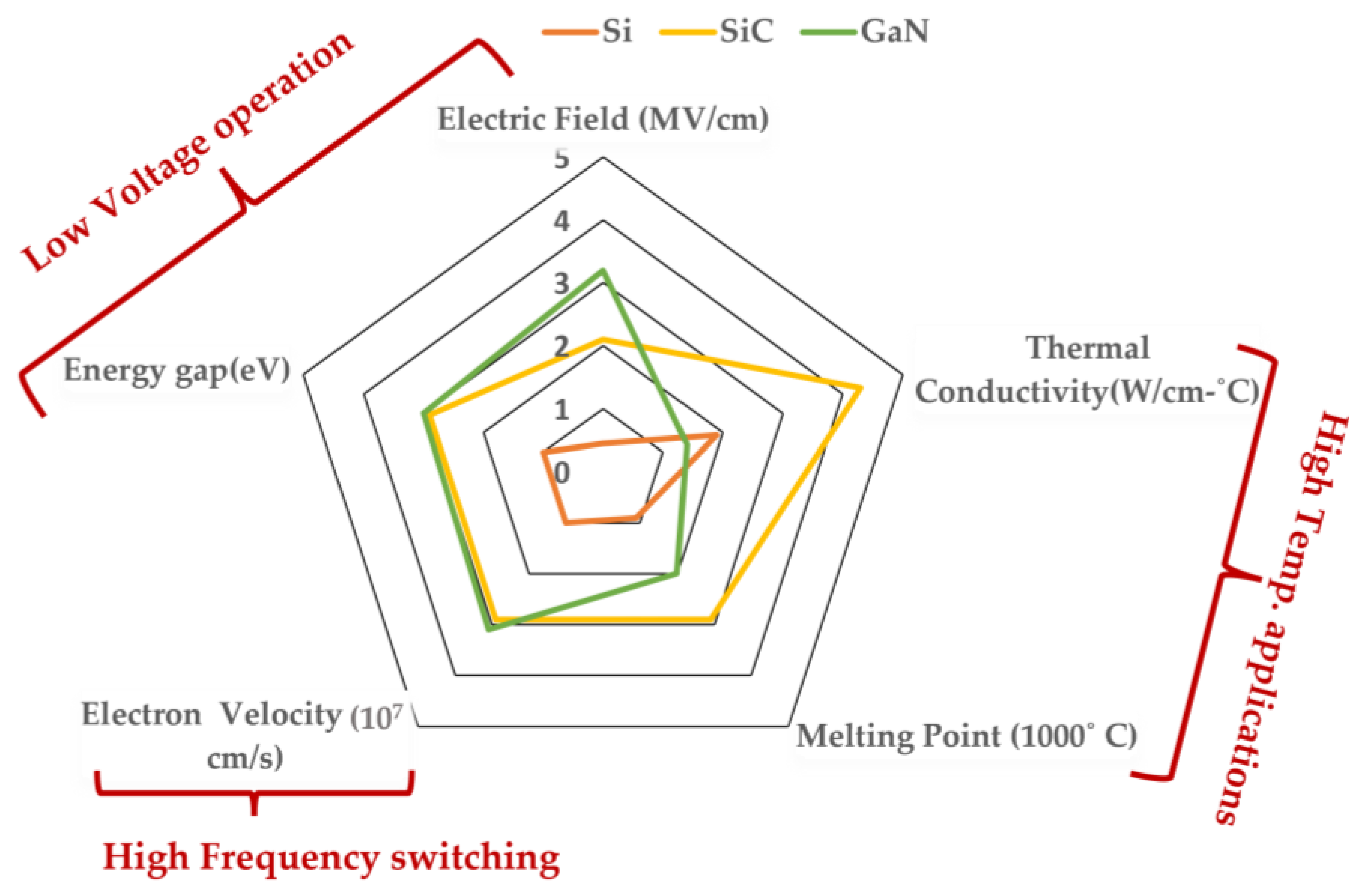
Figure 1. Summary of Si’s, SiC’s, and GaN’s relevant material properties.
SiC is the third hardest substance on earth and is known to be as hard as a single crystal. The SiC energy gap ranges from 2 to 3.3 eV depending on the polytype crystal structure. SiCs are the ideal choice among commercially available WBG devices due to their greater power rating, quicker switching frequency, much lower switching losses, and capacity to handle higher junction temperatures than Si-based devices. Another promising wide bandgap semiconductor material GaN [16][17][18][19] is an example of the third generation of semiconductor materials, with a wider bandgap (bandgap width of more than 3.4 eV), high critical breakdown electric field, high anti-radiation ability, and rapid electron saturation velocity. GaN material has a wide range of applications and is one of the most efficient ways to save energy and reduce consumption worldwide. It summarizes recent research on GaN technology, demonstrating the slow but steady development of a local GaN supply chain.
Wide bandgap power electronic semiconductors are now in the state of active research and development. Researchers are constantly investigating novel device architectures, packaging methods, and heat management strategies to improve further the performance, reliability, and efficiency of wide bandgap devices. These initiatives tackle issues including enhancing device dependability, cutting manufacturing costs, and boosting system-level integration. Wide bandgap power electronic semiconductor applications are also being expanded into new markets, including 5G wireless communications, the Internet of Things (IoT), and sophisticated medical equipment. Wide bandgap devices thrive in these applications because they need excellent power density, quick switching times, and high-frequency functioning.
Ultrawide bandgap (UWBG) semiconductors like diamond enable incredibly promising electrical gadgets. Diamond has a band gap of 5.5 eV broad, more than five times that of Si [17]. Diamond transistor devices can theoretically switch at frequencies over 100 GHz and function at temperatures higher than 600 °C. High-power diamond Schottky diodes for power electronics, diamond UV detectors for monitoring flames, and diamond radiation detectors for physics research are a few unusual applications. Diamond’s excellent heat conductivity and breakdown voltage enable incredibly small, effective power devices. The difficulties in doping diamonds to create trustworthy ohmic connections and the constraints in manufacturing large single-crystal diamond wafers are obstacles to developing diamond electronics. However, in situ-doped polycrystalline diamond films and diamond-on-Si techniques are advancing the field [17]. Diamond has the potential for orders of magnitude of improvements in power density, operating temperature, radiation hardness, and switching speed compared to traditional electronics. Deep space missions to power grid electronics could benefit from revolutionary applications if the diamond’s full potential is realized. Due to their high-efficiency power conversion, electric vehicles have longer driven ranges and require less time to charge. Utilizing wide bandgap technology, renewable energy systems like solar and wind power may maximize energy collecting and grid integration [18]. Moreover, their high-power density and enhanced thermal management capabilities are advantageous for aerospace and defense applications.
2. Si
The preceding discussion demonstrates that Si power devices remain the workhorse technology in power electronics applications despite rising competition from WBG power devices. Si is a Group 14 (IVA) member in the periodic table of elements. Si is also part of the carbon family. These family elements include C, Ge, Sn, and Pb. Si is a metalloid, one of only a few elements with metal and nonmetal properties. Aside from oxygen, Si is the second most abundant element on Earth’s crust. Si was established in 1960 by the 11th General Conference on Weights and Measures, CGPM, Conférence Générale des Poids ET Mesures [19]. The CGPM is the international authority that ensures the wide dissemination of Si and modifies it as necessary to reflect the latest advances in science and technology. It has a diamond cubic crystal structure with a lattice parameter of 0.543 nm [20].
Being a semiconductor, the element, ceramics, and bricks are used for making transistors. It is a vital component of Portland cement. Si materials are used in components of electronic devices. It also makes solar cells [21][22][23][24][25] and parts for computer circuits [26]. A solar cell is a device that converts sunlight into electrical energy [27][28][29][30]. A rectifier is an electrical device that converts alternating current to direct current. The most important Si alloys are those made with Fe, Al, and Cu. When Si is produced, scrap iron and metal are sometimes added to the furnace [31][32]. Several waterproofing systems employ Si as a component for water purification. Si is used in many mold release agents and molding compounds. It is also a component of ferroSi—an alloy widely used in the steel industry.
2.1. Si Diode
For many years, Si diode power semiconductors have been crucial in several applications because of their dependable and effective rectification capabilities. Low forward voltage drops, high current-carrying capacity, and exceptional thermal stability are all positive traits of Si diodes [33]. Their extensive use can be ascribed to their proven dependability records, cost efficiency, and sophisticated production methods. Numerous devices, such as power supplies, inverters, rectifiers, and voltage regulators, use Si diodes. The Si Power Rapid Diode family bridges the gap between SiC diodes. Examples of such Si diodes are previously released emitter-controlled diodes and Infineon’s existing high-power 600 V/650 V diode. Moreover, the TRENCHSTOP™ 5 and high-speed 3 IGBT (Insulated Gate Bipolar Transistor) and CoolMOSTM are good partners for the Rapid 1 and Rapid 2 diodes [34]. For usage in automotive, industrial power control, power management, sensor solutions, and security in Internet of Things applications, Infineon Technologies provides a comprehensive selection of ready-to-use semiconductor design solutions and reference schematics. Si diodes are ultra- and hyper-fast and have outstanding performance with a voltage range of 600–1200 V [35].
As mentioned earlier, the gap between SiC diodes and emitter-controlled diodes is filled by the Rapid 1 and Rapid 2 power Si diodes, which are a complement to the current high-power 600 V/650 V diodes. The new families of hyper- and ultra-fast diodes provide exceptional efficiency and dependability while striking the ideal balance between price and performance. The additional 50 V provides higher reliability.
The 650 V Rapid 1 Diode: The Rapid 1 diode series has the lowest conduction losses, and the smooth recovery minimizes EMI emissions with a 1.35 V temperature-stable forward voltage (FV). The equipment is ideal for power factor correction (PFC) topologies, frequently used in large home appliances like air conditioners and washers.
The 650 V Rapid 2 Diode: The family of Rapid 2 diodes is designed for applications switching between 40 kHz and 100 kHz by providing a low reverse recovery charge (Qrr) and time (trr) to reduce the reverse conduction times associated with the power switch turn-on losses and to provide maximum efficiency [36].
2.2. Si MOSFET
MOSFETs are extensively utilized power semiconductors that have completely changed the power electronics industry. FETs) have become the most significant device in the semiconductor industry due to Lilienfeld’s 1930 [37] patent on the idea and Kahng and Atalla’s 1960 [38] practical implementation of Si/Si dioxide. The development of this industry has been characterized by an exponential pattern known as Moore’s law over the past seven decades [39]. Today’s metal-oxide-semiconductor field-effect transistor (MOSFET) has undergone several modifications, evolving from a single-gate planar MOSFET to a multiple-gate non-planar MOSFET. Nevertheless, it has been and will continue to be the mainstay of the semiconductor industry for the foreseeable future.
MOSFETs made of Si rely on modulating the conductive channel that forms between a semiconductor layer’s source and drain terminals. The device’s bulk is a Si substrate that has been extensively doped; the gate insulator is a thin Si dioxide layer. A voltage applied to the gate terminal generates an electric field that regulates the channel’s conductivity. A positive voltage repels the majority carriers (for an N-channel MOSFET, electrons) from the channel, resulting in a depletion area and decreasing the conductivity of the channel [40]. Applying a negative voltage draws in most of the carriers and improves the conductivity of the channel. The MOSFET may change between the ON state (conducting) and the OFF state (non-conducting) by varying the gate voltage. This idea makes it possible to effectively manage the MOSFET’s ability to handle power and current flow. These components have low on-resistance and can handle large voltages and currents, making efficient power conversion and control possible [6]. The conductivity of Si MOSFETs may be precisely controlled by using a thin Si dioxide layer as the gate insulator. They offer quick switching times, little gate drive needs, and superior thermal performance.
Input capacitance Ciss and on-state resistance Rds(on) grow along with the current rating, whereas gate-drain capacitance Cgd remains mostly constant. A 2.5 A MOSFET, for example, has a Ciss of 1800 pF and Rds(on) of 0.3, whereas a 40 A device has a Ciss of 10,000 pF and Rds(on) of 0.05. Across different power MOSFETs, a trade-off exists between a higher current capability and electrical characteristics such as input capacitance and on-resistance. Moreover, this table illustrates how Si power MOSFET specs and performance scale across various current ratings.
Several sectors, including the automobile, renewable energy, industrial automation, and telecommunications, use Si MOSFETs extensively. The subject of power electronics has been profoundly influenced by Si MOSFETs, which are incredibly adaptable and dependable power semiconductors. Si MOSFETs have evolved into crucial components in various applications, from automotive and renewable energy to industrial automation and telecommunications, because of their low on-resistance, high voltage and current handling capacity, and quick switching rates. They are a popular option for power electronic systems due to their superior thermal performance and compatibility with well-known production techniques, ensuring effective power conversion and control. The widespread use of Si MOSFETs demonstrates how important a role they have played in boosting the overall performance and dependability of power electronic systems and devices. They are the favored option for power electronic systems due to their dependability, high efficiency, and compatibility with established production methods.
2.3. Si SuperJunction MOSFET
To break the Si 1-D constraint, the super-junction (SJ) concept for vertical power devices was established in the mid-1990s [41][42][43]. When the device is turned off, a vertical P layer or P column is introduced to compensate for the charges in the N drift layer. This approach is highly similar to the RESURF concept [44], which has been used in various lateral power devices. The drift area of these devices has a special design that alternates P- and N-type regions, allowing for a more even dispersion of the electric field. For high-power applications, the SuperJunction design lowers on-resistance and boosts efficiency. SJ MOSFETs are designed to reduce the electric field concentration and provide improved voltage-blocking capabilities by forming a depletion area with several tiny cells [45].
Moreover, lower conduction losses, quicker switching times, and enhanced thermal properties are all improved by this design. As a result, the electric field in an SJ device has changed from a triangle to a blue rectangular form, and the N drift layer doping has increased. Forming the vertical P column is the most difficult part of making SJ MOSFET. There are two popular methods, both of which are commercially employed. Si SJ MOSFETs have gained significant attention in power electronics, particularly in applications such as power supplies, LED lighting, and motor drives. Their advanced design and improved efficiency contribute to higher power density and system performance. As a result, Si SJ MOSFETs are rarely used in applications that need a third-quadrant operation, such as voltage source inverters.
2.4. Si IGBT
Si IGBTs are critical power semiconductors that have transformed the field of power electronics. These power devices have revolutionized by combining the advantages of MOSFETs and bipolar junction transistors (BJTs) [46]. They offer high voltage and current handling capabilities while maintaining low on-state voltage drop and fast switching speeds. The structure of a Si IGBT comprises three layers: an N-type collector, a P-type base, and an N-type emitter. By regulating the conductivity of the base region through the voltage applied to the gate terminal, the IGBT enables efficient power switching. The performance and efficiency of Si IGBTs have recently been improved for various applications. One key development is integrating cutting-edge trench gate architectures and novel cell designs. These developments have improved switching speeds, decreased on-state losses, and reduced conduction losses. Furthermore, recent research has concentrated on improving the thermal management of the IGBT, enabling better power densities and increased reliability [47]. Due to improvements in power conversion efficiency, increased power density, and system performance, they are now more appropriate for various applications, including electric cars, renewable energy systems, and industrial automation.
Additionally, current Si IGBT advances have concentrated on reaching greater voltage ratings while lowering power losses. One significant development is using cutting-edge gate-driving methods and cell structure optimization in IGBTs. These developments have increased voltage ratings, decreased conduction and switching losses, and enhanced efficiency [48]. Advanced production methods and materials have also made it possible for better thermal management, which has increased power density and enhanced dependability. The latest advancements in Si IGBT technology have opened the door for creating smaller and more effective power electronic systems in various sectors.
The main features and specifications of popular Si power semiconductor devices, such as BJTs, diodes, MOSFETs, IGBTs, and thyristors. For instance, Si IGBTs have medium conduction, high switching, and overall high-power losses while operating up to 1.2 kV blocking voltage and 50 A current rating. They work well in situations requiring medium voltage and medium frequency. In contrast, despite their slow switching speed, Si thyristors can handle high-voltage, low-frequency applications with up to 4 kV voltage and 3000 A current capacity. Si MOSFETs, which have a blocking voltage of 600 V and a current rating of 100 A, as well as minimal conduction and switching losses, fill the low-voltage, high-frequency market niche. Each Si device has defined features based on its advantages; however, it is constrained by the characteristics.
3. Silicon Carbide (SiC)
SiC is a semiconducting material with outstanding physical, chemical, and electrical properties, making it very suitable for fabricating high-power, low-loss semiconductor devices. Moreover, commercially available SiC devices have lower switching/conduction loss, superior thermal stability, and greater temperature tolerance. SiC devices are, therefore, a very promising alternative to converters designed for high-temperature applications [49]. SiC power electronic devices have a theoretically allowed junction temperature of 600 °C due to the semiconductor’s wide bandgap, around three times that of Si material [50]. On the other hand, the fabrication of these devices is rather intricate owing to the same properties of SiC, like its chemical inertness and hardness. It took over a hundred years to develop SiC electronics up to its modern state when power SiC devices possessing higher efficiency than their Si counterparts became commercially available and widely used in numerous applications. The resistance of the SiC material to an electric field is ten times greater than the resistance of the Si. As a result, SiC devices could be considered capable of withstanding the same blocking voltage with a 10-times-thinner material [51].
A tetrahedral crystalline structure is formed when each Si atom shares its electrons with four carbon atoms. Different SiC poly varieties can be made from this fundamental structure. Shown as Figure 2, SiC is the only chemical compound of group IV elements. It has a strictly stoichiometric concentration ratio of Si and carbon (C) atoms. It should not be mixed with solid solutions, which may be formed by other group IV elements and may have variable component concentration ratios (e.g., SixGe1-x) [52].
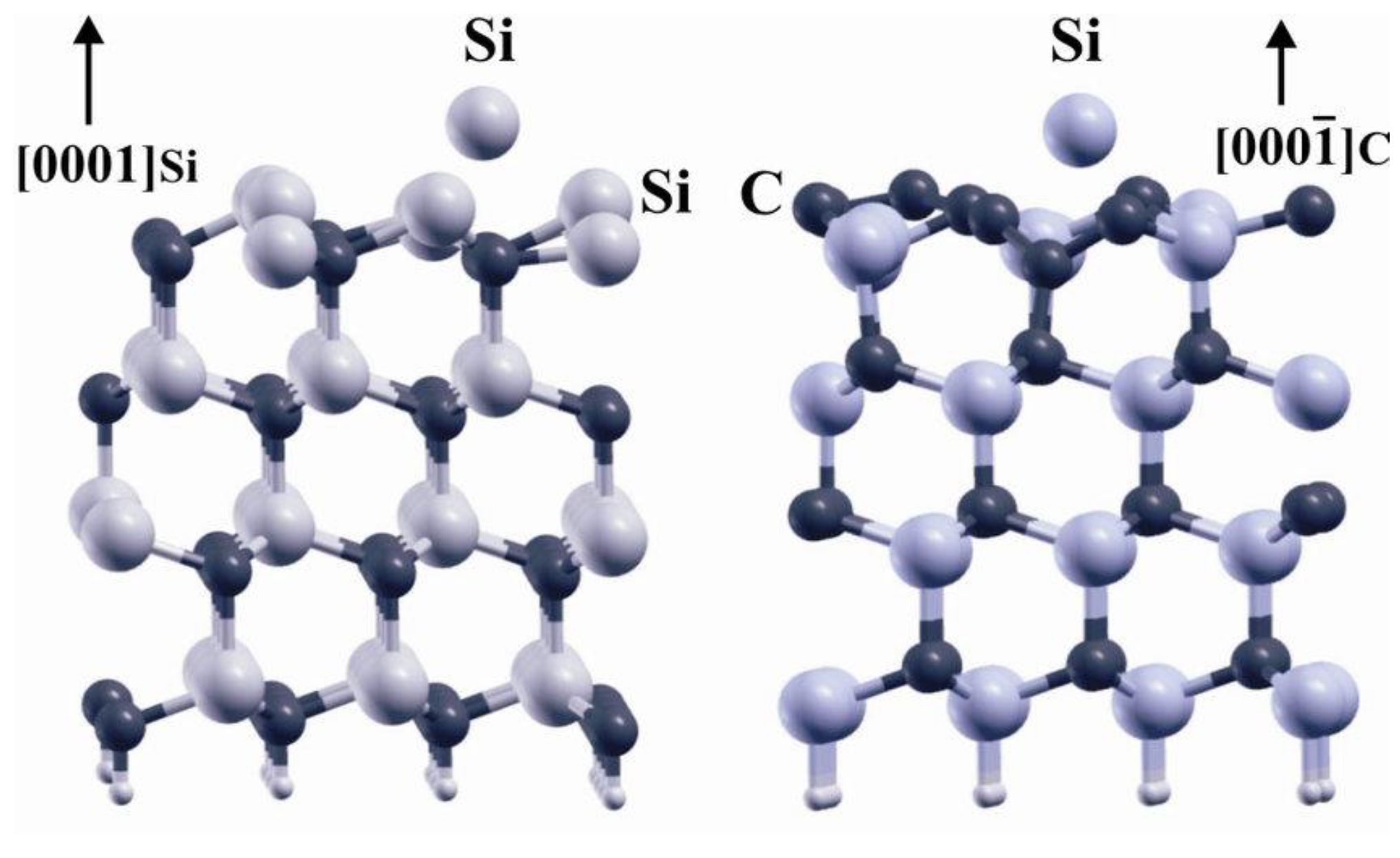
Figure 2. Side view of SiC lattice.
SiC devices can operate at higher switching dynamics. The thermal energy required for an electron to pass from the valence band to the conduction band (forming an electron-hole pair) is considerable in WBG materials. As a result, even at high junction temperatures, the WBG device’s electric characteristics are retained within defined bounds. This enables SiC semiconductor devices to function at high temperatures. Currently, the operating temperature range for SiC devices on the market is between 200 °C and 300 °C [53]. Therefore, SiCs are the ideal choice among commercially available WBD devices due to their greater power rating, quicker switching frequency, much lower switching losses, and capacity to handle higher junction temperatures than Si-based devices [52].
3.1. Discovery of SiC
As previously mentioned, SiC is an excellent material for high-power electronics and high-temperature applications because it has a wide bandgap and good thermal stability [54]. However, 2D SiC offers incredible new features missing from bulk SiC materials due to quantum confinement and surface effects [55][56][57]. SiC has arguably had the longest history of all the semiconducting materials used in electronics. SiC was found as a manufactured material, which makes its discovery exceptional in and of itself. Jöns Jacob Berzelius (1779–1848), in his 1824 report, most likely made the first observation of a chemical molecule bearing Si–C bonds [58]. He could conduct experiments in peculiar settings because of his acknowledged expertise in experimental methods. He also discovered several new chemical elements, including Si, and many other accomplishments. Berzelius made the extremely cautious claim that he had identified a substance that, when burned, created an equal number of Si and carbon atoms [59].
Seventy years later, the first validated SiC synthesis took place by chance [60]. American engineer Edward Goodrich Acheson (1856–1931) experimented with a newly developed electrical furnace in 1891 to create synthetic diamonds (highly demanded by the industry as an abrasive material) [24]. B. I. Ozernikova and A. P. Bobrievich discovered the first naturally occurring SiC of terrestrial origin in sediments of the Tyung River (Siberia) in 1956 and diamond-bearing kimberlite pipes in Yakutia, USSR, respectively, in 1957 [61].
3.2. Material Growth
Wide bandgap semiconductor SiC has outstanding features that make it highly sought-after for various applications. Epitaxy, the process through which SiC crystals grow, is essential for creating high-performance electronics. Chemical vapor deposition (CVD) and physical vapor transfer (PVT) are two growth techniques that have been used [62]. In CVD, SiC is deposited on a substrate due to the high-temperature decomposition of a precursor gas that contains Si and carbon. SiC source material in PVT is sublimated and recrystallizes onto a colder substrate. To produce high-quality single-crystal SiC, both processes require exact temperature control and a suitable growing environment. Growth rate, shape, and crystal quality are influenced by temperature gradients, gas flow rates, and crystal orientation [63]. Larger, higher-quality SiC crystals with fewer flaws have been made possible by improvements in growth methods and equipment, allowing for the manufacture of power electronic devices, high-frequency devices, and sensors that provide greater performance and efficiency compared to conventional materials [64]. The widespread use of SiC in several technological applications will be facilitated by further research and development efforts in SiC growing processes, which promise future improvements in crystal quality, scalability, and cost-effectiveness.
3.3. SiC Diode
Due to the greater SiC dielectric critical field than its Si counterparts, a blocking voltage rise of 10 times above that of Si is achievable with the same thickness of the SiC drift layer. Compared to Si diodes, SiC’s high thermal conductivity has several benefits, including the ability to operate at higher current density ratings and reduce the size of cooling systems. SiC SBDs have been commercially available since 2001 and have continuously increased in the blocking voltage and conduction current ratings. There are essentially three types of SiC power diodes [65]. The PN junction and the Schottky Barrier Diode (SBD) junction are two semiconductor mechanisms that can create a diode, and there is no conductivity modulation in the SBD. From 600 V to 10 kV, Si PN junction diodes dominate the market. The scenario is fully reversed in the case of SBD on WBG material, such as SiC. The high critical electric field Ec in SiC reduces the resistance of an SBD significantly. As a result, conductivity modulation is neither necessary nor desirable. Because SBD does not store any charge, it can achieve near-zero reverse recovery loss. As a result, a WBG diode based on the Schottky mechanism is nearly optimal. The junction barrier Schottky (JBS) diode structure, which provides an area to shield the Schottky region in a reverse blocking state, can be used to reduce leakage current.
The PN junction of the JBS diode can become conductive at a high forward bias, giving it a stronger surge capability than the SBD [66]. On the other hand, the SiC PN junction diode will have to overcome a forward voltage drop of roughly 3 V across the PN junction, making it exceedingly undesirable from the standpoint of conduction loss, even if the drift area resistance can be decreased via conductivity modulation. The JBS structure is typically used in SiC diodes above 600 V. Because the off-state leakage current in JBS is decreased, devices can be rated at temperatures as high as 175 °C. Majority of the carrier electrons still are used for device conduction, and advantages of the SiC PIN diode over JBS or SBD is its substantially lower leakage current, which makes it an ideal option for high-voltage and high-temperature operation.
3.4. SiC MOSFET
SiC power MOSFETs are quickly gaining widespread application. Reliability issues like bias temperature instability and gate oxide cracking are mostly under control [67]. It is the chosen SiC three-terminal switch due to the well-established gate-driving technique and user base in Si MOSFET and IGBT compared to SiC JFET and BJT. It is commercially available in voltages ranging from 650 V to 1700 V, with higher current (5–600 A) modules [68]. SiC MOSFETs provide clear prospects for improving operating frequency, efficiency, and power density, but their employment is complicated by several unwanted side effects brought on by their rapid switching speed [69]. SiC MOSFETs can achieve relatively low on-resistances—0.013 Ohms for an 80 A device, which enable high-frequency switching, but at the expense of greater input and gate capacitances than Si MOSFETs.
When compared to the IGBT system, the operation frequency of SiC MOSFET-based converters has increased by one or two orders of magnitude, as demonstrated in Figure 3. SiC MOSFETs can also achieve zero switching loss under specific situations. A 1.2 kV SiC MOSFET module was recently proven to operate at 3.38 MHz [70][71]. The P regions shelter the gate oxide in the planar structure, so the peak electric field near the oxide is decreased. The gate-oxide stability problem in planar MOSFETs has been overcome, and high-reliability performance has been attained [72].
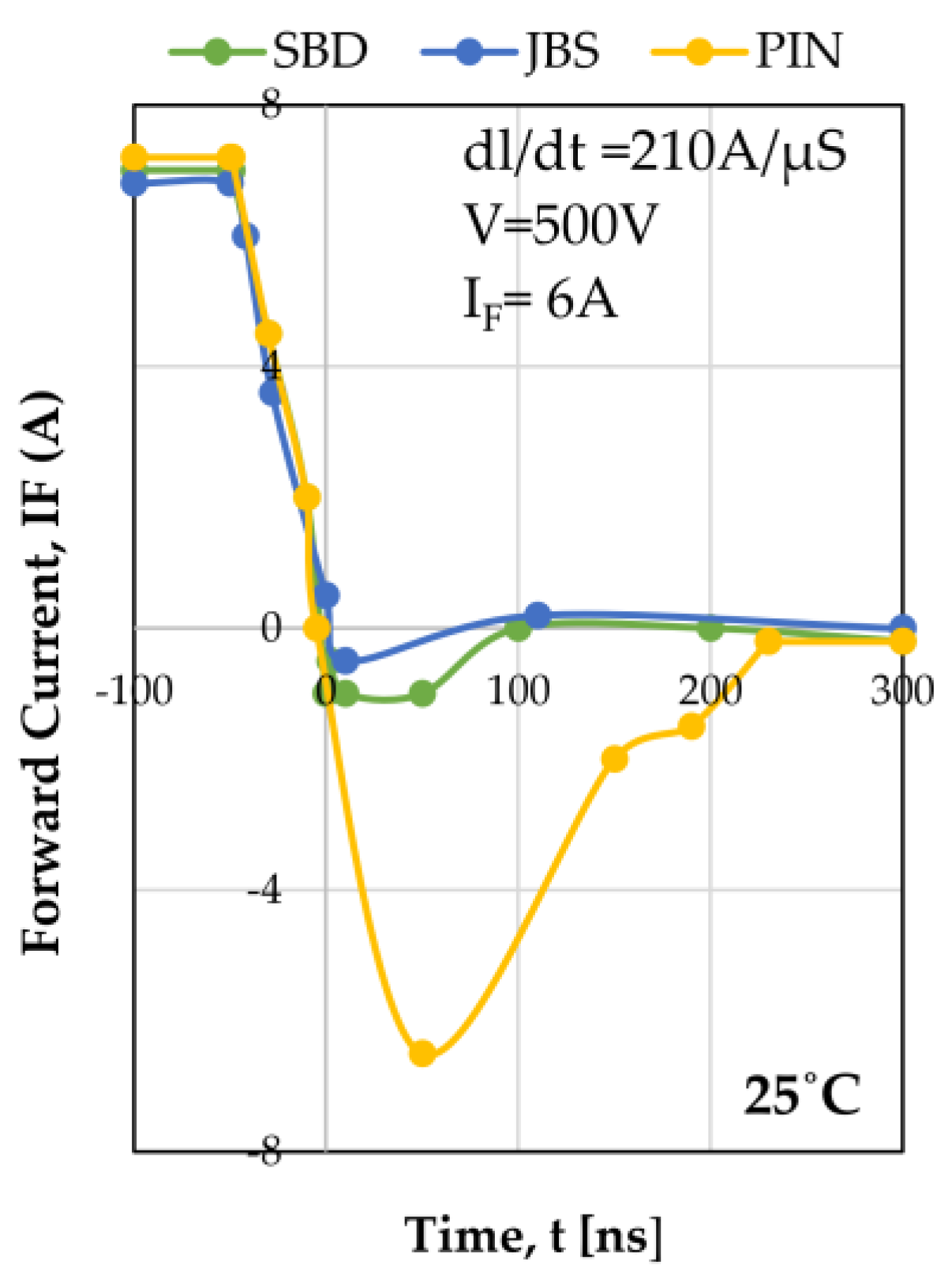
Figure 3. SiC diodes’ turn-off current waveforms at 25 °C inductive load.
General Electric (GE) also exhibited the industry’s first dependable SiC MOSFET with a 200 °C junction temperature [73][74]. This is more difficult in the trench device. Many different trench structures exist to protect the trench gate’s bottom [75][76][77][78][79][80]. Another key motivator for SiC MOSFET innovation, in addition to enhancing electrical performance, is reliability. The three key criteria for evaluating dependability are high-temperature gate bias, high-temperature reverse bias, and high-humidity, high-temperature reverse bias. One of the most important challenges in the fabrication of SiC-MOSFETs was the lack of a reliable insulator for the gate terminal. A proper insulator is needed to achieve stable forward I–V characteristics and a stable gate threshold voltage. For this reason, the SiC-MOSFET was commercialized later than the SiC-JFET. Most MOSFETs contain a PIN diode inherent to their structure. This diode has a forward bias voltage around 2.5 V. During the conduction of the body diode, if the MOSFET is turned on, the forward characteristic of the body diode can be virtually improved, and, thus, the conduction losses are reduced. Figure 4 shows the calculated converter efficiency for a 1200-V SiC MOSFET system versus that is based on an IGBT/SiC diode hybrid power module. These graphs are critical for designing power converters for various applications.
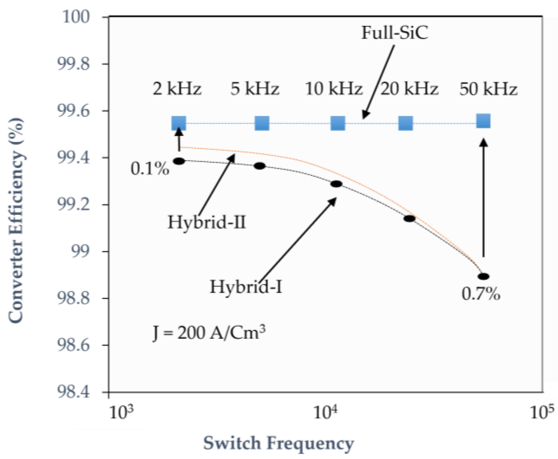
Figure 4. Calculated converter efficiency for a 1200-V SiC MOSFET system versus that based on an IGBT/SiC diode hybrid power module.
Switches, solenoids, encoders, generators, and electric motors are the primary electromechanical devices that connect the digital and physical worlds. The capacity of each of these gadgets to translate electrical impulses into mechanical motions is what gives them their enchantment. The need for more control, efficiency, and capabilities from these electromechanical devices rises as fields like automated manufacturing, electronic vehicles, sophisticated building systems, and smart appliances develop [81]. It investigates how improvements in SiC MOSFETs are expanding the possibilities of electric motors, which hitherto relied on Si IGBTs for power inversion. Similar to the new power electronic converters, SiC devices could be utilized for motor driver applications for novel electric machines for various applications [82][83][84][85][86][87]. This development increases the potential of motor drive applications across all industries.
The cabling between the drive inverters and the motor driver may be significantly reduced by bringing the motor driver assembly to the motor’s local position, resulting in considerable cost savings. Figure 5 shows seven motors of a robotic arm, that is required to be powered by 21 different cables, which might require hundreds of meters of costly and intricate cabling infrastructure, in a typical Si IGBT power cabinet. Two lengthy cables that link to each motor’s motor drive within the local motor assembly can be used in a SiC MOSFET motor drive system to decrease the number of cables [81]. There are specific applications where IGBTs may still be better suited, as is true for all types of components; however, SiC MOSFET inverters offer several distinct advantages over Si IGBTs, making them very attractive solutions for motor drive and a wide range of other applications.
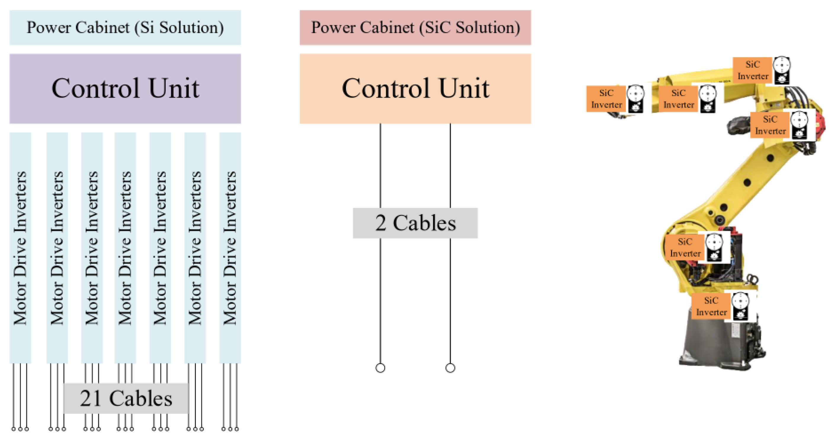
Figure 5. Comparison of a Si IGBT vs. SiC MOSFET system control of a robot arm.
3.5. SiC IGBT
SiC IGBT has received a lot of interest in the domains of high voltage transmission, smart grid, and pulse power since it is the highest voltage switch. SiC IGBTs have not been commercialized because of their inherent flaws and crude manufacturing methods. The stated SiC IGBT devices’ exceptional static and dynamic performance and significant dv/dt during hard switching challenge the power conversion system. SiC IGBT has a lot of potential solutions; however, comparisons with Si IGBT and SiC MOSFET reveal significant discrepancies. The potential SiC IGBT appears to have a chance to displace Si devices in the future based on early experiments in high-voltage fields.
High voltage direct current transmission (HVDC), industrial applications, traction systems, and new pulsed power applications are the key markets for Si IGBT with high voltage and current. Ultra-high voltage in these domains is intended to decrease the number of devices connected in series and simplify converter topologies [88]. According to one source, Si IGBTs can withstand a maximum voltage of 8.4 kV [89], which is about as high as Si devices can go. The continued advancement of Si IGBT in these sectors is also severely constrained by frequency and operating temperature. SiC exhibits greater breakdown field strength, inherent temperature, thermal conductivity, and carrier saturation drift velocity as a wide bandgap material [90]. The SiC IGBT with 4H-polytype and n-channel is chosen among SiC polytypes and channel types because it has a low forward voltage (Vf), quick switching, and a large safe working region. Wide-base PNP transistors in 4H-SiC N-IGBTs have excellent bulk mobility and low current gain, contributing to a favorable trade-off between Vf and switching loss.
SiC IGBTs have a lower Vf than Si IGBTs under the same blocking capability but have lower bulk mobility than Si IGBTs. Even though SiC IGBTs have not yet been commercialized, significant advancements have been made over the previous 30 years, as seen in Figure 1. Because of the readily accessible n+ substrate with low resistivity and defect density, the SiC p-channel IGBT has been widely investigated from 1996 when the first SiC IGBT was produced [91] through 2010. Continuous improvements have been made to the P-IGBT’s performance, notably since the charge storage layer (CSL) was introduced [92]. Due to immature technology and a P-type substrate with a high resistivity and defect density during this time, the constructed N-channel IGBT performs poorly [93].
Because free-standing technology offers a way to develop a P+ collector on an N+ substrate, the research focus of SiC IGBT shifted to SiC N-channel IGBT before Cooper’s freestanding technology proposal in 2010 [94]. After that, SiC N-IGBT displays ever-improving static and dynamic properties. The SiC IGBT has a blocking voltage that exceeds 27 kV [95], making it a promising device in high-voltage areas. In comparison to the SiC MOSFET of the same rated voltage, the SiC IGBT might cut the differential specific on-resistances (Ron,sp,diff) by more than one order of magnitude. Therefore, even if the switching loss (Esw) of the SiC IGBT is larger than that of SiC MOSFET, it is promising for power conversion systems with more than 100 kW transmission power. Recently, the first solid-state transformer prototypes and the first Marx generators have also been made using the 12–15 kV SiC IGBT modules that were developed [96][97][98].
SiC-IGBTs are more effective than Si-IGBTs because of their switching speed. The gate-to-emitter voltage rise quickly to allow for the SiC-IGBT to switch quickly. Therefore, to charge the input capacitance Ciss, a greater gate current is needed [99]. Generally, to switch the IGBT off, the gate current capability is increased by reducing the external turn-on and turn-off gate resistors even though the same current capability is needed. In order for the gate current to rise as quickly as required, the gate driver’s stray inductance must also be kept to a minimum [100]. SiC-IGBTs need a negative gate-to-emitter voltage like that found in Si-IGBTs to obtain a quick and secure turn-off transient. A SiC-IGBT driver typically supplies a gate-to-emitter voltage of +20 V positive and 5 V negative [101].
SiC devices outperform Si in high-voltage, high-frequency applications like PV inverters, EV systems, and power supplies. It compares parameters like bandgap, electron mobility, voltage/current ratings, switching frequency, power losses, and figures of merit. The table shows the compromises made by various SiC devices for application-specific performance optimization.
3.6. Applications and Emergence of SiC Power Electronics
SiC is employed in semiconducting and other items such as armored vehicles, ceramic plates, thin filament pyrometry, foundry crucibles, and auto clutches. SiC was initially used in electrical applications as a lightning arrester in a high-voltage power system because engineers and scientists realized SiC works well even in the presence of high volts and high temperatures. SiC devices are appropriate for a wide range of applications in aerospace and space missions [102][103], despite the necessity for high-temperature dependable device packaging to be developed [104][105]. Schottky diodes, MOSFETs, and power electronics are some of the most recent electrical devices that use SiC.
Applications for SiC include sandblasting injectors, automobile water pump seals, bearings, pump parts, and extrusion dies. These applications use SiC’s exceptional hardness, abrasion resistance, and corrosion resistance [106]. SiC is undoubtedly durable and versatile, with applications ranging from semiconductors for Schottky diodes to use as an abrasive polishing material. Its exceptional qualities include sublimation, great chemical inertness and corrosion resistance, excellent thermal characteristics, and the capacity to develop as a single-crystal structure.
The introduction of the first mass-produced electrical vehicles (EVs) to the market in 2008—Tesla Motors’ debut of its first all-electric vehicle—significantly impacted the development of SiC power electronics. Two components of the electrical power train significantly impact the performance of these cars. They are an inverter and a battery charger that transform the DC power from a battery pack into AC power for a motor. Since the battery capacitance in EVs restricts the amount of on-board stored energy, the efficiency of power conversion by these units is crucial. The bulk of modern electric vehicles (EVs) and the first electric vehicles (EVs) used inverters with Si IGBTs and conversion efficiencies ranging from 80% to 95%. Even at 95% efficiency, these inverters waste too much energy and need liquid cooling. Compared to the electrical motors, they are bigger and heavier. The conversion efficiency of the inverter might be increased to 99% [107] by swapping Si IGBTs for SiC MOSFETs while being significantly lighter and smaller. The first commercial SiC power MOSFET was introduced by Cree, Inc. in 2011 [108]. This potential use of SiC power devices in the high-volume automotive sector sparked increased research into the design and technology of SiC devices.
Tesla introduced the Model 3 in 2017, the first electric vehicle to have inverters based on SiC MOSFETs. By the time this article was published, each week’s manufacturing of automobiles used 48 SiC MOSFETs with a 650 V/100 A rating made at the STMicroelectronics fab in Catania, Italy [109]. At the same time, Tesla Model 3’s traction motor spins at 17,900 revolutions per minute, and China’s NEV Technology Roadmap 2.0 aims to reach a motor speed of 25,000 rotations per minute by 2035 [110]. DENSO, a global automotive manufacturer, built its first inverter using SiC semiconductors. The new Lexus RZ, a Toyota luxury brand’s first specifically designed battery electric vehicle (BEV) model, will employ this inverter, which is part of the eAxle, an electric drive module designed by BluE Nexus Corporation [111]. It appears that Toyota is producing its first BEV in large quantities through the Lexus Division. SiC and GaN are competing to see which is superior for power electronics. They both outperform Si in either situation.
The market for SiC power devices is expanding rapidly, and the SiC industrial sector today exhibits significant diversity, with successful businesses operating in various ways. This predicts that SiC power electronics will continue to flourish as an industrial technology during the coming several decades. The enormous potential of SiC as a material for high-temperature and high-frequency electronics, which is still not realized and is awaiting convincing demonstration of SiC’s superiority over conventional semiconductors for these applications, is another factor driving the further development of SiC technology.
Over the past 13 years, GE Aviation has committed over $150 million to developing SiC technology, solidifying its position as the market leader. Because of characteristics like high-temperature tolerance, low losses, and higher frequencies, SiC enables lighter, more effective, and higher-performance power electronics. To reach extremely high-power density and efficiency goals, GE is utilizing SiC technology in aerospace applications, including hybrid electric aircraft propulsion. GE can create lighter and more potent systems for electric ground vehicles and other applications due to SiC. GE Aviation is well-positioned to promote SiC power device adoption moving ahead due to its extensive aerospace knowledge and experience.
The SiC-based generator controller developed by GE Aerospace shows a significant advancement in power electronics when compared to industrial Si-based generator controllers. Its benefits are glaringly obvious in many important areas. First off, the SiC controller is extraordinarily effective at harvesting and managing electrical power within a small footprint due to an amazing fourfold improvement in power density relative to its size. With a twofold increase in power density per unit weight, its power-to-weight ratio is also improved, which results in both increased efficiency and a decrease in the overall weight of the controller. This drop is accompanied by a 50% reduction in physical size, highlighting SiC’s promise for applications that conserve space. Notably, the SiC-based controller excels at increasing conversion efficiency. It increases DC/AC conversion efficiency from 94% to an astounding 99%, guaranteeing little energy is lost in the process. Similarly, it improves efficiency in DC/DC conversions from 84% to 95%, maximizing power transfer. SiC technology improves efficiency in AC/DC conversions from 85% to 92%, leading to more effective power conversion and energy use.
Figure 6 shows the evaluation of SiC modules and SiC technology utilized in aerospace applications by GE Aerospace in conjunction with Power America, the Department of Energy, and the National Renewable Energy Laboratory. The modules have voltage ratings of 1200 V and 1700 V and come in half-bridge, dual-bridge, six-switch, and six-pack versions. Ratings range from 425 A to 1425 A. On-state resistance, thermal resistance, size, and maximum junction temperature are important factors mentioned. With small footprints up to 100 mm × 140 mm and operational temperatures up to 175 °C, the table demonstrates great power density and temperature capability of SiC modules. SiC modules can be configured in a wide range of ways to accommodate various power electronic circuit topologies and the current/voltage ratings needed for aviation applications.
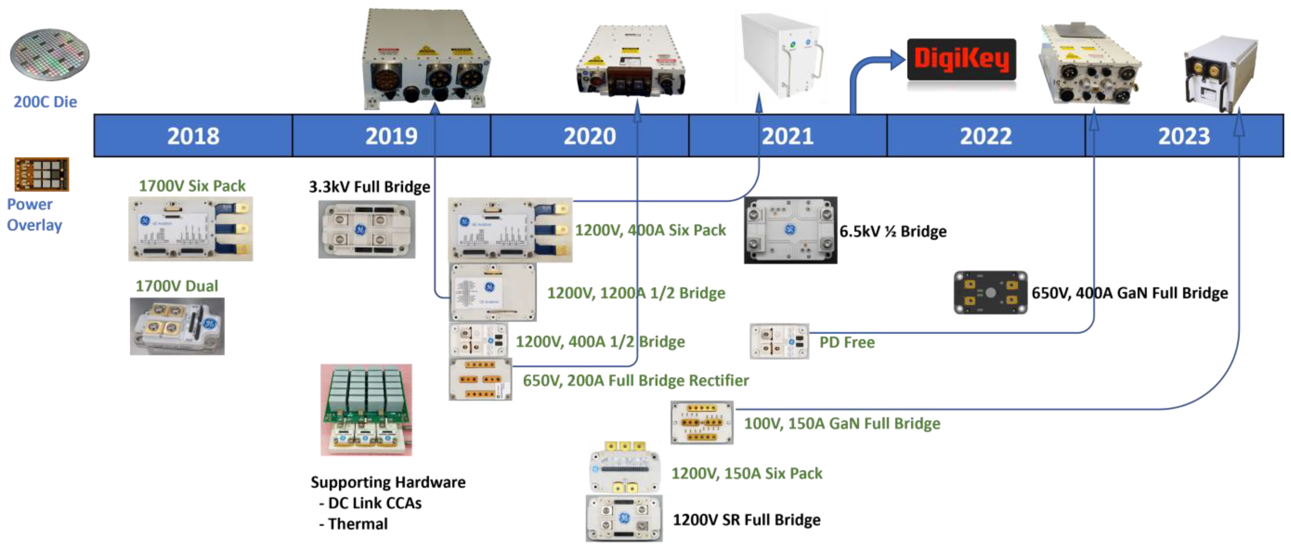
Figure 6. Evaluation of wideband power semiconductor modules designed and manufactured by GE Aerospace.
References
- Rafin, S.M.S.H.; Ahmed, R.; Mohammed, O.A. Wide Band Gap Semiconductor Devices for Power Electronic Converters. In Proceedings of the 2023 Fourth International Symposium on 3D Power Electronics Integration and Manufacturing (3D-PEIM), Miami, FL, USA, 1–3 February 2023; pp. 1–8.
- Palmour, J.W. SiC power device development for industrial markets. In Proceeding of the IEEE International Electron Devices Meeting (IEDM) 2014, San Francisco, CA, USA, 15–17 December 2014; pp. 1.1.1–1.1.8.
- Chow, T.P. Progress in high voltage SiC and GaN power switching devices. Mater. Sci. Forum 2014, 778-780, 1077–1082.
- Rafin, S.M.S.H.; Islam, R.; Mohammed, O.A. Power Electronic Converters for Wind Power Generation. In Proceedings of the 2023 Fourth International Symposium on 3D Power Electronics Integration and Manufacturing (3D-PEIM), Miami, FL, USA, 1–3 February 2023; pp. 1–8.
- Rafin, S.M.S.H.; Haque, M.A.; Islam, R.; Mohammed, O.A. A Review of Power Electronic Converters for Electric Aircrafts. In Proceedings of the 2023 Fourth International Symposium on 3D Power Electronics Integration and Manufacturing (3D-PEIM), Miami, FL, USA, 1–3 February 2023; pp. 1–8.
- Zerarka, M.; Austin, P.; Toulon, G.; Morancho, F.; Arbess, H.; Tasselli, J. Behavioral study of single-event burnout in power devices for natural radiation environment applications. IEEE Trans. Electron Devices 2012, 59, 3482–3488.
- Yu, C.-H.; Wang, Y.; Liu, J.; Sun, L.-L.J.I.T.o.E.D. Research of single-event burnout in floating field ring termination of power MOSFETs. IEEE Trans. Electron. Devices 2017, 64, 2906–2911.
- Carr, J.A.; Hotz, D.; Balda, J.C.; Mantooth, H.A.; Ong, A.; Agarwal, A. Assessing the impact of SiC MOSFETs on converter interfaces for distributed energy resources. IEEE Trans. Power Electron. 2009, 24, 260–270.
- Alam, M.; Kumar, K.; Dutta, V. Comparative efficiency analysis for Si, SiC MOSFETs and IGBT device for DC–DC boost converter. SN Appl. Sci. 2019, 1, 1700.
- Biela, J.; Schweizer, M.; Waffler, S.; Kolar, J.W. SiC versus Si—Evaluation of potentials for performance improvement of inverter and DC–DC converter systems by SiC power semiconductors. IEEE Trans. Ind. Electron. 2010, 58, 2872–2882.
- Chow, T.P. SiC and GaN high-voltage power switching devices. Mater. Sci. Forum 2000, 338–342, 1155–1160.
- Guo, Y.-B.; Bhat, K.P.; Aravamudhan, A.; Hopkins, D.C.; Hazelmyer, D.R. High current and thermal transient design of a SiC SSPC for aircraft application. In Proceedings of the 2011 Twenty-Sixth Annual IEEE Applied Power Electronics Conference and Exposition (APEC), Fort Worth, TX, USA, 6–11 March 2011; pp. 1290–1297.
- Nakamura, T.; Sasagawa, M.; Nakano, Y.; Otsuka, T.; Miura, M. Large current SiC power devices for automobile applications. In Proceedings of the 2010 International Power Electronics Conference-ECCE ASIA-, Sapporo, Japan, 21–24 June 2010; pp. 1023–1026.
- Ranjbar, A. Applications of Wide Bandgap (WBG) Devices in the Transportation Sector. Recent Advances in (WBG) Semiconductor Material (e.g. SiC and GaN) and Circuit Topologies. In Transportation Electrification: Breakthroughs in Electrified Vehicles, Aircraft, Rolling Stock, and Watercraft; IEEE: Piscataway, NJ, USA, 2022; pp. 47–72.
- Roccaforte, F.; Fiorenza, P.; Greco, G.; Nigro, R.L.; Giannazzo, F.; Iucolano, F.; Saggio, M.J. Emerging trends in wide band gap semiconductors (SiC and GaN) technology for power devices. Microelectron. Eng. 2018, 187, 66–77.
- Chen, K.J.; Häberlen, O.; Lidow, A.; lin Tsai, C.; Ueda, T.; Uemoto, Y.; Wu, Y. GaN-on-Si power technology: Devices and applications. IEEE Trans. Electron Devices 2017, 64, 779–795.
- Tsao, J.; Chowdhury, S.; Hollis, M.; Jena, D.; Johnson, N.; Jones, K.; Kaplar, R.; Rajan, S.; Van de Walle, C.; Bellotti, E. Ultrawide-bandgap semiconductors: Research opportunities and challenges. Adv. Electron. Mater. 2018, 4, 1600501.
- Al Mamun, M.; Paudyal, S.; Kamalasadan, S. Efficient Dynamic Simulation of Unbalanced Distribution Grids with Distributed Generators. In Proceedings of the 2023 IEEE Industry Applications Society Annual Meeting, Nashville, TN, USA, 29 October–2 November 2023; pp. 1–6.
- National Institute of Standards and Technology (NIST). Available online: https://www.nist.gov/pml/owm/metric-si/understanding-metric (accessed on 29 September 2023).
- Zulehner, W. Historical overview of Si crystal pulling development. Mater. Sci. Eng. 2000, 73, 7–15.
- Zaidi, B. Introductory chapter: Introduction to photovoltaic effect. Sol. Panels Photovolt. Mater. 2018, 1–8.
- Zaidi, B.; Hadjoudja, B.; Felfli, H.; Chouial, B.; Chibani, A. Effet des traitements thermiques sur le comportement électrique des couches de silicium polycristallin pour des applications photovoltaïques. Rev. De Métallurgie 2011, 108, 443–446.
- Goetzberger, A.; Knobloch, J.; Voss, B. Crystalline Si Solar Cells; Wiley Online Library: Hoboken, NJ, USA, 1998; Volume 1.
- Zaidi, B.; Hadjoudja, B.; Felfli, H.; Chibani, A. Influence of doping and heat treatments on carriers mobility in polycrystalline Si thin films for photovoltaic application. Turk. J. Phys. 2011, 35, 185–188.
- Mathieu, H.; Bretagnon, T.; Lefebvre, P. Physique des Semiconducteurs et des Composants Electroniques-Problèmes Résolus; Dunod: Malakoff, France, 2001.
- Zaidi, B.; Saouane, I.; Shekhar, C. Electrical energy generated by amorphous Si solar panels. Si 2018, 10, 975–979.
- Zaidi, B.; Saouane, I.; Shekhar, C. Simulation of single-diode equivalent model of polycrystalline Si solar cells. Int. J. Mater. Sci. Appl. 2018, 7.
- Conibeer, G. Third-generation photovoltaics. Mater. Today 2007, 10, 42–50.
- Zaidi, B.; Belghit, S.; Shekhar, C.; Mekhalfa, M.; Hadjoudja, B.; Chouial, B. Electrical performance of CuInSe2 solar panels using ant colony optimization algorithm. J. Nano-Electron. Phys. 2018, 10, 05045.
- Sigfússon, T.I.; Helgason, Ö. Rates of transformations in the ferroSi system. Hyperfine Interact. 1990, 54, 861–867.
- Waanders, F.; Mans, A. Characterisation of ferroSi dense medium separation material. Hyperfine Interact. 2003, 148, 325–329.
- Borysiuk, J.; Sołtys, J.; Bożek, R.; Piechota, J.; Krukowski, S.; Strupiński, W.; Baranowski, J.M.; Stępniewski, R. Role of structure of C-terminated 4 H-SiC (000 1−) surface in growth of graphene layers: Transmission electron microscopy and density functional theory studies. Phys. Rev. B 2012, 85, 045426.
- Baliga, B.J. Power Semiconductor Devices. Brooks/Cole. 1995. Available online: https://www.abebooks.com/servlet/BookDetailsPL?bi=31307574601 (accessed on 29 September 2023).
- Ultra- and Hyper-Fast Si Diodes: 650V Rapid 1 and Rapid 2. Available online: https://www.infineon.com/cms/en/product/power/diodes-thyristors/Si-diodes/650v-rapid-1-and-rapid-2/ (accessed on 29 September 2023).
- Infenion. Available online: https://www.infineon.com/cms/en/product/power/diodes-thyristors/Si-diodes/600v-1200v-ultra-soft/ (accessed on 29 September 2023).
- Moller, H. Semiconductors for Solar Cells; Artech House Inc.: Norwood, MA, USA, 1993.
- Edgar, L.J. Method and Apparatus for Controlling Electric Currents. US Patent 1,745,175, 21 January 1930.
- Kahng, D. Si-Si dioxide field field induced surface devices. In Proceedings of the IRE-AIEE Solid-State Device Research Conference, Pittsburgh, PA, USA, 1960; Available online: https://scholar.google.com/scholar_lookup?title=Silicon%E2%80%93Silicon%20Dioxide%20Field%20Induced%20Surface%20Devices&author=D.K.%20State&publication_year=1960 (accessed on 29 September 2023).
- Moore, G.E. Cramming more components onto integrated circuits. IEEE 1998, 86, 82–85.
- Sze, S.M.; Ng, K.K. Physics of Semiconductor Devices; John Wiley & Sons: Hoboken, NJ, USA, 2007.
- Deboy, G.; Marz, N.; Stengl, J.-P.; Strack, H.; Tihanyi, J.; Weber, H. A new generation of high voltage MOSFETs breaks the limit line of Si. In Proceedings of the International Electron Devices Meeting 1998. Technical Digest (Cat. No. 98CH36217), San Francisco, CA, USA, 6–9 December 1998; pp. 683–685.
- Fujihira, T.; Miyasaka, Y. Simulated superior performances of semiconductor superjunction devices. In Proceedings of the 10th International Symposium on Power Semiconductor Devices and ICs. ISPSD’98 (IEEE Cat. No. 98CH36212), Kyoto, Japan, 3–6 June 1998; pp. 423–426.
- Chen, X.B. Breakthrough to the" Si limit" of power devices. In Proceedings of the 1998 5th International Conference on Solid-State and Integrated Circuit Technology, Beijing, China, 23 October 1998; pp. 141–144.
- Appels, J.; Vaes, H. High voltage thin layer devices (RESURF devices). In Proceedings of the 1979 International Electron Devices Meeting, Washington, DC, USA, 3–5 December 1979; pp. 238–241.
- Udrea, F.; Deboy, G.; Fujihira, T. Superjunction Power Devices, History, Development, and Future Prospects. IEEE Trans. Electron Device 2017, 64, 713–727.
- Baliga, B.J. Insulated Gate Bipolar Transistors (IGBTs): Theory and Design; World Scientific Publishing: Singapore, 2003.
- VolLaska, T. Progress in Si IGBT Technology – as an ongoing Competition with WBG Power Devices. In Proceeding of the 2019 IEEE International Electron Devices Meeting (IEDM), San Francisco, CA, USA, 7–11 December 2019; pp. 12.2.1–12.2.4.
- Vobecký, J. Design and technology of high-power Si devices. In Proceedings of the 18th International Conference Mixed Design of Integrated Circuits and Systems—MIXDES 2011, Gliwice, Poland, 16–19 June 2011; pp. 17–22.
- Guo, X.; Xun, Q.; Li, Z.; Du, S. SiC converters and MEMS devices for high-temperature power electronics: A critical review. Micromachines 2019, 10, 406.
- Tian, Y.; Zetterling, C.-M. A fully integrated Si-carbide Sigma–Delta modulator operating up to 500 °C. IEEE Trans. Electron Devices 2017, 64, 2782–2788.
- Garrido-Diez, D.; Baraia, I. Review of wide bandgap materials and their impact in new power devices. In Proceedings of the 2017 IEEE International Workshop of Electronics, Control, Measurement, Signals and Their Application to Mechatronics (ECMSM), Donostia, Spain, 24–26 May 2017; pp. 1–6.
- Li, K. Wide Bandgap (SiC/GaN) Power Devices Characterization and Modeling: Application to HF Power Converters. Ph.D. Thesis, École Doctorale Sciences pour L’ingénieur (Lille), Lille, France, 2014.
- Chen, C.; Luo, F.; Kang, Y. A review of SiC power module packaging: Layout, material system and integration. CPSS Trans. Power Electron. Appl. 2017, 2, 170–186.
- Chabi, S.; Kadel, K. Two-dimensional SiC: Emerging direct band gap semiconductor. Nanomaterials 2020, 10, 2226.
- Susi, T.; Skákalová, V.; Mittelberger, A.; Kotrusz, P.; Hulman, M.; Pennycook, T.J.; Mangler, C.; Kotakoski, J.; Meyer, J.C. Computational insights and the observation of SiC nanograin assembly: Towards 2D SiC. Sci. Rep. 2017, 7, 4399.
- Ferdous, N.; Islam, M.S.; Park, J.; Hashimoto, A. Tunable electronic properties in stanene and two dimensional Si-carbide heterobilayer: A first principles investigation. AIP Adv. 2019, 9, 025120.
- Chowdhury, C.; Karmakar, S.; Datta, A. Monolayer group IV–VI monochalcogenides: Low-dimensional materials for photocatalytic water splitting. J. Phys. Chem. C 2017, 121, 7615–7624.
- Berzelius, J.J. Untersuchungen über die Flussspathsäure und deren merkwürdigsten Verbindungen. Ann. Der Phys. 1824, 77, 169–230.
- Pensl, G.; Ciobanu, F.; Frank, T.; Krieger, M.; Reshanov, S.; Schmid, F.; Weidner, M. Sic material properties. In Sic Materials And Devices; World Scientific: Singapore, 2006; Volume 1, pp. 1–41.
- Acheson, E.G. Carborundum: Its history, manufacture and uses. J. Frankl. Inst. 1893, 136, 279–289.
- Kaminskiy, F.; Bukin, V.; Potapov, S.; Arkus, N.; Ivanova, V. Discoveries of SiC under natural conditions and their genetic importance. Int. Geol. Rev. 1969, 11, 561–569.
- Choyke, W.J.; Patrick, L.; Ziegler, J. (Eds.) SiC 2: Materials, Processing, and Devices; Springer: Berlin/Heidelberg, Germany, 2018.
- Kimoto, T.; Cooper, J.A. Fundamentals of SiC Technology: Growth, Characterization, Devices and Applications; John Wiley & Sons: Hoboken, NJ, USA, 2014.
- Zhang, Y.; Suzuki, T. Epitaxial Growth of SiC—Review on Growth Mechanism and Technology. J. Cryst. Growth 2019, 512, 1–22.
- Singh, R.; Capell, D.C.; Hefner, A.R.; Lai, J.; Palmour, J.W. High-power 4H-SiC JBS rectifiers. IEEE Trans. Electron. Devices 2002, 49, 2054–2063.
- Huang, X.; Wang, G.; Lee, M.-C.; Huang, A.Q. Reliability of 4H-SiC SBD/JBS diodes under repetitive surge current stress. In Proceedings of the 2012 IEEE Energy Conversion Congress and Exposition (ECCE), Raleigh, NC, USA, 15–20 September 2012; pp. 2245–2248.
- Cheung, K.P. SiC power MOSFET gate oxide breakdown reliability—Current status. In Proceedings of the 2018 IEEE International Reliability Physics Symposium (IRPS), Burlingame, CA, USA, 11–15 March 2018; pp. 2B. 3-1–2B. 3-5.
- Wang, J.; Jiang, X. Review and analysis of SiC MOSFETs’ ruggedness and reliability. IET Power Electron. 2020, 13, 445–455.
- She, X.; Huang, A.Q.; Lucia, O.; Ozpineci, B. Review of SiC power devices and their applications. IEEE Trans. Ind. Electron. 2017, 64, 8193–8205.
- Guo, S.; Zhang, L.; Lei, Y.; Li, X.; Xue, F.; Yu, W.; Huang, A.Q. 3.38 Mhz operation of 1.2 kV SiC MOSFET with integrated ultra-fast gate drive. In Proceedings of the 2015 IEEE 3rd Workshop on Wide Bandgap Power Devices and Applications (WiPDA), Blacksburg, VA, USA, 2–4 November 2015; pp. 390–395.
- Pérez-Tomás, A.; Brosselard, P.; Hassan, J.; Jorda, X.; Godignon, P.; Placidi, M.; Constant, A.; Millán, J.; Bergman, J. Schottky versus bipolar 3.3 kV SiC diodes. Semicond. Sci. Technol. 2008, 23, 125004.
- Langpoklakpam, C.; Liu, A.-C.; Chu, K.-H.; Hsu, L.-H.; Lee, W.-C.; Chen, S.-C.; Sun, C.-W.; Shih, M.-H.; Lee, K.-Y.; Kuo, H.-C. Review of SiC processing for power MOSFET. Crystals 2022, 12, 245.
- Losee, P.; Bolotnikov, A.; Yu, L.; Beaupre, R.; Stum, Z.; Kennerly, S.; Dunne, G.; Sui, Y.; Kretchmer, J.; Johnson, A. 1.2 kV class SiC MOSFETs with improved performance over wide operating temperature. In Proceedings of the 2014 IEEE 26th International Symposium on Power Semiconductor Devices & IC’s (ISPSD), Waikoloa, HI, USA, 15–149 June 2014; pp. 297–300.
- DiMarino, C.M.; Burgos, R.; Dushan, B. High-temperature SiC: Characterization of state-of-the-art SiC power transistors. IEEE Ind. Electron. Mag. 2015, 9, 19–30.
- Qingwen, S.; Xiaoyan, T.; Yimeng, Z.; Yuming, Z.; Yimen, Z. Investigation of SiC trench MOSFET with floating islands. IET Power Electron. 2016, 9, 2492–2499.
- Jiang, H.; Wei, J.; Dai, X.; Ke, M.; Deviny, I.; Mawby, P. SiC trench MOSFET with shielded fin-shaped gate to reduce oxide field and switching loss. IEEE Electron. Device Lett. 2016, 37, 1324–1327.
- Hiyoshi, T.; Uchida, K.; Sakai, M.; Furumai, M.; Tsuno, T.; Mikamura, Y. Gate oxide reliability of 4H-SiC V-groove trench MOSFET under various stress conditions. In Proceedings of the 2016 28th international Symposium on Power Semiconductor devices and ics (iSPSd), Prague, Czech Republic, 12–16 June 2016; pp. 39–42.
- Song, Q.; Yang, S.; Tang, G.; Han, C.; Zhang, Y.; Tang, X.; Zhang, Y.; Zhang, Y. 4H-SiC trench MOSFET with L-shaped gate. IEEE Electron. Device Lett. 2016, 37, 463–466.
- Wang, Y.; Tian, K.; Hao, Y.; Yu, C.-H.; Liu, Y.-J. An optimized structure of 4H-SiC U-shaped trench gate MOSFET. IEEE Trans. Electron Devices 2015, 62, 2774–2778.
- Takaya, H.; Morimoto, J.; Hamada, K.; Yamamoto, T.; Sakakibara, J.; Watanabe, Y.; Soejima, N. A 4H-SiC trench MOSFET with thick bottom oxide for improving characteristics. In Proceedings of the 2013 25th International Symposium on Power Semiconductor Devices & IC’s (ISPSD), Kanazawa, Japan, 26–30 May 2013; pp. 43–46.
- Arrow. Available online: https://www.arrow.com/en/research-and-events/articles/advantages-of-sic-mosfet-vs-si-igbt (accessed on 29 September 2023).
- Rafin, S.M.S.H.; Mohammed, O.A. Novel Dual Inverter Sub-Harmonic Synchronous Machines. IEEE Trans. Magn. 2023, 59, 8202605.
- Rafin, S.M.S.H.; Ali, Q.; Mohammed, O.A. Hybrid Sub-Harmonic Synchronous Machines Using Series and Parallel Consequent Permanent Magnet. In Proceedings of the 2023 IEEE Energy Conversion Congress and Exposition (ECCE), Nashville, TN, USA, 29 October – 2 November 2023; pp. 1–5.
- Rafin, S.M.S.H.; Ali, Q.; Mohammed, O.A. Novel PM-Assisted Model of the Two-Layer Sub-Harmonic Synchronous Machines. In Proceedings of the 2023 International Applied Computational Electromagnetics Society Symposium (ACES), Monterey/Seaside, CA, USA, 26–30 March 2023; pp. 1–2.
- Rafin, S.M.S.H.; Mohammed, O.A. Sub-Harmonic Synchronous Machine Using a Dual Inverter and a Unique Three-Layer Stator Winding. In Proceedings of the 2023 IEEE International Magnetic Conference-Short Papers (INTERMAG Short Papers), Sendai, Japan, 15–19 May 2023; pp. 1–2.
- Rafin, S.M.S.H.; Ali, Q.; Lipo, T.A. A novel sub-harmonic synchronous machine using three-layer winding topology. World Electr. Veh. J. 2022, 13, 16.
- Rafin, S.M.S.H.; Ali, Q.; Khan, S.; Lipo, T.A. A novel two-layer winding topology for sub-harmonic synchronous machines. Electr. Eng. 2022, 104, 3027–3035.
- Kadavelugu, A.; Mainali, K.; Patel, D.; Madhusoodhanan, S.; Tripathi, A.; Hatua, K.; Bhattacharya, S.; Ryu, S.-H.; Grider, D.; Leslie, S. Medium voltage power converter design and demonstration using 15 kV SiC N-IGBTs. In Proceedings of the 2015 IEEE Applied Power Electronics Conference and Exposition (APEC), Charlotte, NC, USA, 15–19 March 2015; pp. 1396–1403.
- Rahimo, M.; Kopta, A.; Eicher, S.; Kaminski, N.; Bauer, F.; Schlapbach, U.; Linder, S. Extending the boundary limits of high voltage IGBTs and diodes to above 8 kV. In Proceedings of the 14th International Symposium on Power Semiconductor Devices and Ics, Sante Fe, NM, USA, 7 June 2002; pp. 41–44.
- Wang, G.; Huang, A.Q.; Wang, F.; Song, X.; Ni, X.; Ryu, S.-H.; Grider, D.; Schupbach, M.; Palmour, J. Static and dynamic performance characterization and comparison of 15 kV SiC MOSFET and 15 kV SiC n-IGBTs. In Proceedings of the 2015 IEEE 27th International Symposium on Power Semiconductor Devices & IC’s (ISPSD), Hong Kong, China, 10–14 May 2015; pp. 229–232.
- Ramungul, N.; Chow, T.; Ghezzo, M.; Kretchmer, J.; Hennessy, W. A fully planarized, 6H-SiC UMOS insulated-gate bipolar transistor. In Proceedings of the 1996 54th Annual Device Research Conference Digest, Santa Barbara, CA, USA, 26 June 1996; pp. 56–57.
- Zhang, Q.; Jonas, C.; Callanan, R.; Sumakeris, J.; Das, M.; Agarwal, A.; Palmour, J.; Ryu, S.-H.; Wang, J.; Huang, A. New Improvement Results on 7.5 kV 4H-SiC p-IGBTs with R diff, on of 26 mΩ·cm 2 at 25 °C. In Proceedings of the 19th International Symposium on Power Semiconductor Devices and IC’s, Jeju, Republic of Korea, 27–31 May 2007; pp. 281–284.
- Avram, M.; Brezeanu, G.; Avram, A.; Neagoe, O.; Brezeanu, M.; Iliescu, C.; Codreanu, C.; Voitincu, C. Contributions to development of high power SiC-IGBT. In Proceedings of the CAS 2005 Proceedings. 2005 International Semiconductor Conference, Sinaia, Romania, 3–5 October 2005; pp. 365–368.
- Wang, X.; Cooper, J.A. High-voltage n-channel IGBTs on free-standing 4H-SiC epilayers. IEEE Trans. Electron. Devices 2010, 57, 511–515.
- Van Brunt, E.; Cheng, L.; O’Loughlin, M.J.; Richmond, J.; Pala, V.; Palmour, J.W.; Tipton, C.W.; Scozzie, C. 27 kV, 20 A 4H-SiC n-IGBTs. Mater. Sci. Forum 2015, 821–823, 847–850.
- Madhusoodhanan, S.; Hatua, K.; Bhattacharya, S.; Leslie, S.; Ryu, S.-H.; Das, M.; Agarwal, A.; Grider, D. Comparison study of 12kV n-type SiC IGBT with 10kV SiC MOSFET and 6.5 kV Si IGBT based on 3L-NPC VSC applications. In Proceedings of the 2012 IEEE Energy Conversion Congress and Exposition (ECCE), Raleigh, NC, USA, 15–20 September 2012; pp. 310–317.
- Kadavelugu, A.; Bhattacharya, S.; Ryu, S.-H.; Van Brunt, E.; Grider, D.; Agarwal, A.; Leslie, S. Characterization of 15 kV SiC n-IGBT and its application considerations for high power converters. In Proceedings of the 2013 IEEE Energy Conversion Congress and Exposition, Denver, CO, USA, 15–19 September 2013; pp. 2528–2535.
- Tripathi, A.; Mainali, K.; Madhusoodhanan, S.; Patel, D.; Kadavelugu, A.; Hazra, S.; Bhattacharya, S.; Hatua, K. MVDC microgrids enabled by 15kV SiC IGBT based flexible three phase dual active bridge isolated DC-DC converter. In Proceedings of the 2015 IEEE Energy Conversion Congress and Exposition (ECCE), Montreal, QC, Canada, 20–24 September 2015; pp. 5708–5715.
- Han, L.; Liang, L.; Kang, Y.; Qiu, Y. A Review of SiC IGBT: Models, Fabrications, Characteristics, and Applications. IEEE Trans. Power Electron. 2021, 36, 2080–2093.
- Abdalgader, I.A.; Kivrak, S.; Özer, T. Power performance comparison of SiC-IGBT and Si-IGBT switches in a three-phase inverter for aircraft applications. Micromachines 2022, 13, 313.
- Ciuti, G.; Ricotti, L.; Menciassi, A.; Dario, P. MEMS sensor technologies for human centred applications in healthcare, physical activities, safety and environmental sensing: A review on research activities in Italy. Sensors 2015, 15, 6441–6468.
- Funaki, T.; Balda, J.C.; Junghans, J.; Kashyap, A.S.; Mantooth, H.A.; Barlow, F.; Kimoto, T.; Hikihara, T. Power conversion with SiC devices at extremely high ambient temperatures. IEEE Trans. Power Electron. 2007, 22, 1321–1329.
- Katoh, Y.; Snead, L.L. SiC and its composites for nuclear applications–Historical overview. J. Nucl. Mater. 2019, 526, 151849.
- Ning, P.; Wang, F.; Ngo, K.D. High-temperature SiC power module electrical evaluation procedure. IEEE Trans. Power Electron. 2011, 26, 3079–3083.
- Wang, R.; Boroyevich, D.; Ning, P.; Wang, Z.; Wang, F.; Mattavelli, P.; Ngo, K.D.; Rajashekara, K. A high-temperature sic three-phase ac-dc converter design for> 100/spl deg/c ambient temperature. IEEE Trans. Power Electron. 2012, 28, 555–572.
- Carbosystem. Available online: https://carbosystem.com/en/Si-carbide-properties-applications (accessed on 29 September 2023).
- Zabihi, N.; Mumtaz, A.; Logan, T.; Daranagama, T.; McMahon, R.A. SiC power devices for applications in hybrid and electric vehicles. Mater. Sci. Forum 2019, 963, 869–872.
- Durham, N. Cree Launches Industry’s First Commercial SiC Power Mosfet. 2011. Available online: https://compoundsemiconductor.net/article/87227/Cree_Launches_Industry%E2%80%99s_First_Commercial_SiC_Power_MOSFET (accessed on 29 September 2023).
- STMicroelectronics: STPOWER SiC MOSFETs. Available online: https://www.st.com/en/power-transistors/stpower-sic-mosfets.html (accessed on 29 September 2023).
- Cai, W.; Wu, X.; Zhou, M.; Liang, Y.; Wang, Y. Review and development of electric motor systems and electric powertrains for new energy vehicles. Automot. Innov. 2021, 4, 3–22.
- Greencarcongress. Available online: https://www.greencarcongress.com/2023/04/20230404-denso.html (accessed on 29 September 2023).
More
Information
Subjects:
Engineering, Electrical & Electronic
Contributors
MDPI registered users' name will be linked to their SciProfiles pages. To register with us, please refer to https://encyclopedia.pub/register
:
View Times:
1.8K
Revisions:
2 times
(View History)
Update Date:
13 Nov 2023
Table of Contents


Notice
You are not a member of the advisory board for this topic. If you want to update advisory board member profile, please contact office@encyclopedia.pub.
OK
Confirm
Only members of the Encyclopedia advisory board for this topic are allowed to note entries. Would you like to become an advisory board member of the Encyclopedia?
Yes
No
${ textCharacter }/${ maxCharacter }
Submit
Cancel
Back
Comments
${ item }
|
${ item.createdUser.fullName }
${ item.createdAt }
${ item.vote }
${ item.reply }
Delete
${ reply.createdUser.fullName }
${ reply.createdAt }
${ reply.vote }
Delete
There is no reply to this comment~
${ item.replyTextCharacter }/${ item.replyMaxCharacter }
Submit
Cancel
More
No more~
There is no comment~
${ textCharacter }/${ maxCharacter }
Submit
Cancel
${ selectedItem.replyTextCharacter }/${ selectedItem.replyMaxCharacter }
Submit
Cancel
Confirm
Are you sure to Delete?
Yes
No