Your browser does not fully support modern features. Please upgrade for a smoother experience.
Submitted Successfully!
 +1 credit
Thank you for your contribution! You can also upload a video entry or images related to this topic.
For video creation, please contact our Academic Video Service.
| Version | Summary | Created by | Modification | Content Size | Created at | Operation |
|---|---|---|---|---|---|---|
| 1 | Yue Hao Choong | -- | 5322 | 2023-10-20 08:40:43 | | | |
| 2 | Rita Xu | Meta information modification | 5252 | 2023-10-20 09:32:55 | | | | |
| 3 | Rita Xu | + 9 word(s) | 5261 | 2023-10-24 04:01:12 | | |
Video Upload Options
We provide professional Academic Video Service to translate complex research into visually appealing presentations. Would you like to try it?
Cite
If you have any further questions, please contact Encyclopedia Editorial Office.
Choong, Y.H.; Krishnan, M.; Gupta, M. 3D Printing of Pure Copper Functional Structures. Encyclopedia. Available online: https://encyclopedia.pub/entry/50597 (accessed on 27 July 2026).
Choong YH, Krishnan M, Gupta M. 3D Printing of Pure Copper Functional Structures. Encyclopedia. Available at: https://encyclopedia.pub/entry/50597. Accessed July 27, 2026.
Choong, Yue Hao, Manickavasagam Krishnan, Manoj Gupta. "3D Printing of Pure Copper Functional Structures" Encyclopedia, https://encyclopedia.pub/entry/50597 (accessed July 27, 2026).
Choong, Y.H., Krishnan, M., & Gupta, M. (2023, October 20). 3D Printing of Pure Copper Functional Structures. In Encyclopedia. https://encyclopedia.pub/entry/50597
Choong, Yue Hao, et al. "3D Printing of Pure Copper Functional Structures." Encyclopedia. Web. 20 October, 2023.
Copy Citation
The 3D printing of pure copper to sufficiently high densities has finally taken off, due to the emergence of commercial-grade printers which are now equipped with 1 kW high-power lasers or short-wavelength lasers.
additive manufacturing
heat sink
heat pipe
filigree geometries
1. Introduction
3D printing, also known as additive manufacturing (AM), has gained traction as an industrial manufacturing solution for complex geometry components. This is due to its inherent advantages in the freedom of design and integration of functional parts that result from a layer-by-layer fabrication process. For thermal management devices such as heat sinks and heat exchangers, which consist of multiple fins or internal passageways that are constructed out of thin wall geometries and lattice structures, AM is an appealing alternative to conventional manufacturing processes such as subtractive machining. This is illustrated in Figure 1, which visually highlights the differences in channel geometries for a cold plate heat sink that are possible with AM compared to traditional machining. The AM channels, formed as topology-optimised lattice structures, can increase the amount of surface area that is available for heat transfer within the smallest volume possible, while still facilitating smooth fluid flow with minimal pressure losses in contrast to simpler linear geometries [1].
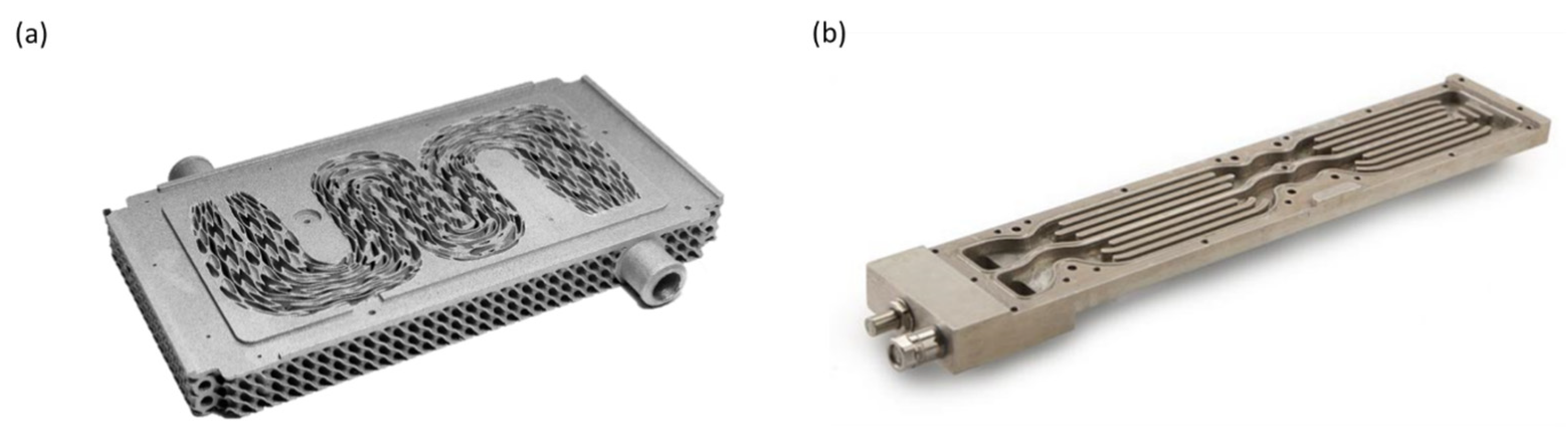
Figure 1. Exposed internal channels of a cold plate heat sink fabricated via (a) additive manufacturing and (b) conventional machining.
Until recently, the development of metal AM hardware and processing technologies has generally focused on improving the performance of structural metals such as steels, nickel alloys, titanium alloys, and aluminium alloys. High levels of dimensional accuracy and geometrical complexity, as well as material properties that are comparable to mature refinement techniques, can now be routinely obtained from various commercial AM solution providers [2][3][4][5][6].
AM technology has progressively matured over the past five years. The recent emergence of industrial-grade 3D printers in the commercial market that are now equipped with higher power 1 kW lasers (100–400 W typical) in the near-infrared (NIR) spectrum (1060 nm) [7], as well as short-wavelength green lasers (515 nm) [8][9] has created new opportunities for manufacturers of thermal management devices to 3D print pure copper beyond the laboratory level. Pure copper, the quintessential material known for its outstanding thermal and electrical conductivities that are approximately double that of aluminium, could previously not be processed via Laser-Powder Bed Fusion (L-PBF), the most widely used metal AM process, to sufficiently high density and conductivities. This is due to the inherently high optical reflectivity of copper to NIR irradiation [10], which is the typical wavelength of laser units used in commercial L-PBF printers. As a result, the complete melting and fusion of the copper feedstock particles cannot occur. In severe cases, stray back-reflections of the laser can result in damages to the optical system of the 3D printer (see Figure 2) [11]. Hence, the lack of printability for copper has hitherto been a major obstacle in the additive fabrication of thermal management devices [12].
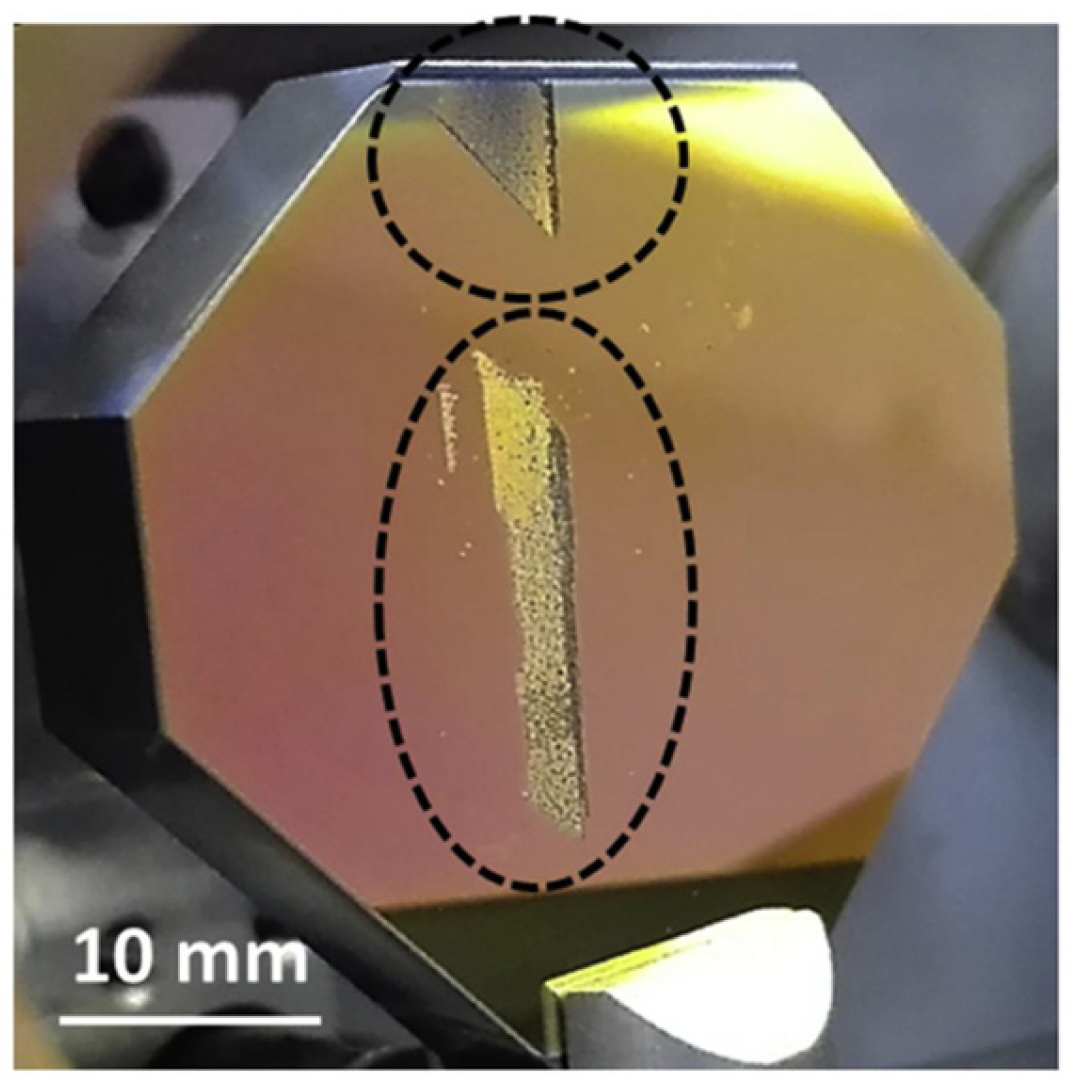
Figure 2. Coating damages to the optical mirror (denoted by dotted outline) of a laser-powder bed fusion printer after being subjected to a 12 h exposure to back-reflections from a bulk copper substrate.
Although the literature on the AM processing of high-purity copper has been recently reviewed by Romano et al. [13], Jiang et al. [14], Campagnoli et al. [15], and Tran et al. [16] between 2019 and 2022, a gap is noted in the concise evaluation of state-of-the-art 3D printing of pure copper functional geometries with fine or filigree features that are specific to thermal management devices. To the best of the authors’ knowledge, the only review on the AM of copper for thermal management applications was previously published in 2017 by Singer et al. [12], before the wider availability of commercial L-PBF printers that are equipped with high-power or short-wavelength lasers.
2. State-of-the-Art in the AM of Pure Copper Filigree Geometries
2.1. Thin-Wall Structures
Recently, in 2019, Guan et al. investigated the L-PBF fabrication of pure copper thin-wall grid-like structures (see Figure 3a) using a typical 1060 nm NIR wavelength laser with a beam spot size of 80 µm [17]. At a laser power of 190 W and scan speed of 500 mm/s, thin walls of 0.2 mm, 0.3 mm, and 0.5 mm thickness were formed. Despite the use of a meander exposure strategy with a hatching distance of 60 µm (see Figure 3b) that imparted additional energy from multiple meltpool overlaps compared to single laser scan tracks, the authors observed that the thin walls consisted primarily of discontinuous meltpool beads that were only partially fused together (see Figure 3c,d). Furthermore, some powder particles could also be found trapped in the cave-like pores formed between adjacent semi-fused beads, especially at the intersections of the grid-like structure (see Figure 3e). To achieve further densification, the authors proposed the use of higher power 500 W lasers in combination with several laser remelting exposure strategies. At the same time, it is also advisable that the energy input should not be overly excessive. This would increase the susceptibility of filigree geometries to the denudation effect [18], whereby the depletion of metal particles occurs in the immediate vicinity of the solidified track and is caused by the outwards meltpool vapor pressure created during laser exposure. When multiple thin walls are closely packed together such as in the case of a mesh structure, the formation of a large denudation zone can result in an uneven powder bed for the next deposited layer.
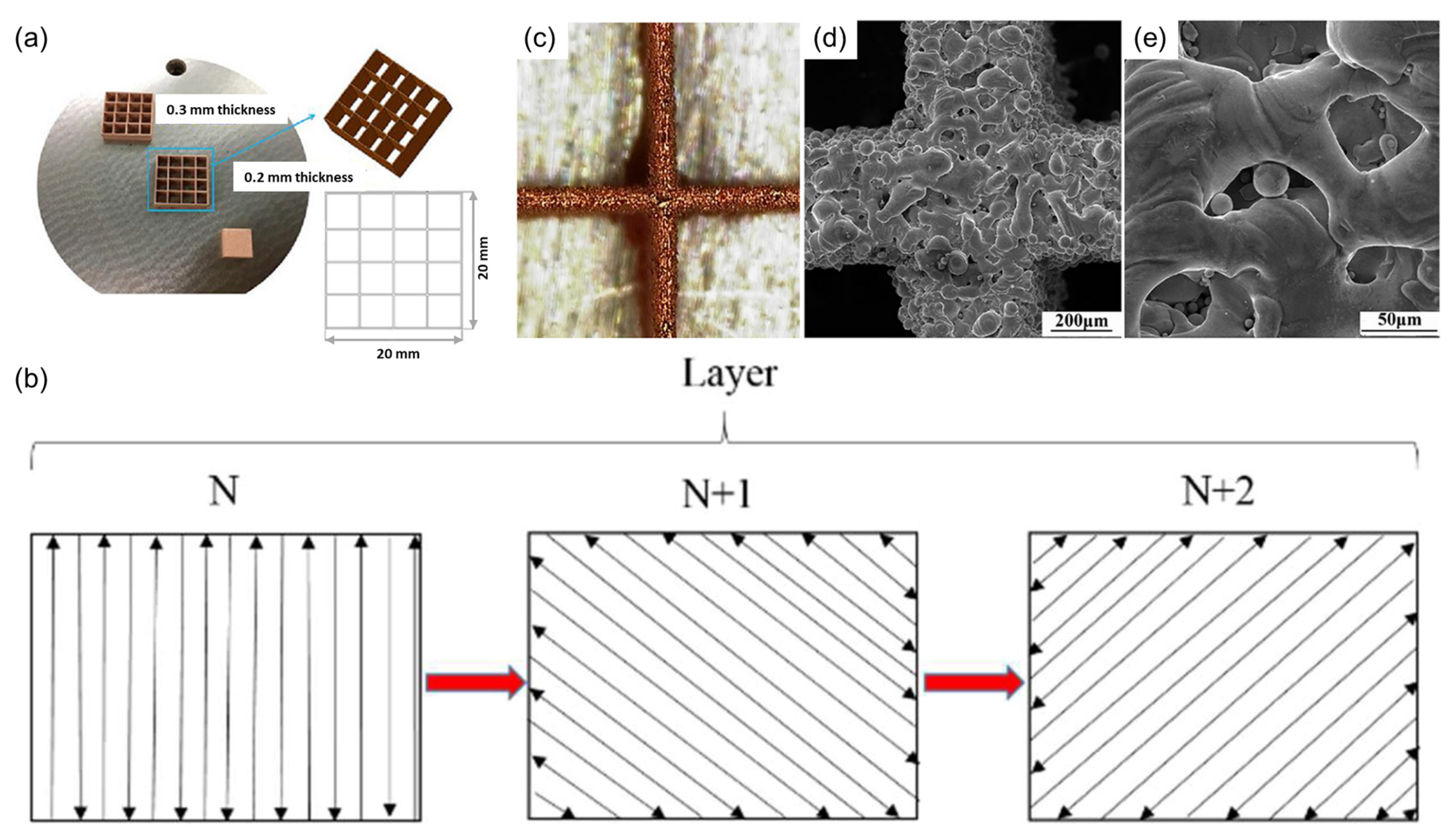
Figure 3. (a) Pure copper thin-wall grid structures with wall thickness of 0.2 mm, 0.3 mm, and 0.5 mm fabricated using NIR L-PBF, (b) meander exposure strategy for three consecutive layers N, N+1, and N+2, (c) close-up optical image of grid structure shown in (a) with porous surface texture, (d) SEM image of grid structure with lack-of-fusion resulting in individual meltpool beads, and (e) SEM image of grid structure node intersection, with trapped spherical particles within cave-like pores.
In the same year, Silbernagel et al. [19] conducted a L-PBF process parameter study on free-standing pure copper thin walls 18 mm in length and 4 mm in height (see Figure 4a). The 3D printer used was equipped with a laser unit of 1070 nm wavelength and beam spot size of 35 µm. The authors investigated three different laser powers of 100 W, 150 W, and 200 W, three different layer thicknesses of 30 µm, 45 µm, and 60 µm, and a scan speed ranging from 150 mm/s to 1250 mm/s in increments of 25 mm/s. Also, instead of the meander exposure strategy used by Guan et al. [17] in the previous study, the authors utilised a single-line laser scan track that was repetitively stacked at every layer to form the planar wall. Hence, the wall thickness would be solely dependent on the size of the meltpool in the powder bed. Regarding layer thickness, the authors observed that the use of 45 µm layers resulted in a good balance of powder spreadability and melting behaviour, therefore it was used for the rest of the study. The 30 µm layers resulted in powder spreading issues, which ultimately resulted in missing sections in the thin walls. Conversely, 60 µm layers resulted in inconsistent meltpool tracks, which exhibited sintering rather than melting characteristics and further indicated that the energy was insufficient for full-depth penetration into the thicker deposited layer. For laser power, the authors found that improvements to the continuity of the thin walls were insensitive to different combinations of laser powers or different orders of those powers, even when multiple scans over the same track were made. In fact, repeated passes at high laser powers resulted only in a detrimental balling effect on the thin walls. Here, the effects of denudation for thin-wall structures when using remelting strategies at high laser powers are re-emphasised. For the scan speeds, the authors found that while the highest, 1250 mm/s, scan speed could provide sufficient energy to form a thin wall, bonding was minimal, which resulted in very thin walls of low strength. Subsequently, by comparing the continuity of the meltpool tracks and wall thickness, the authors were able to identify an optimal scan speed of 300 mm/s.
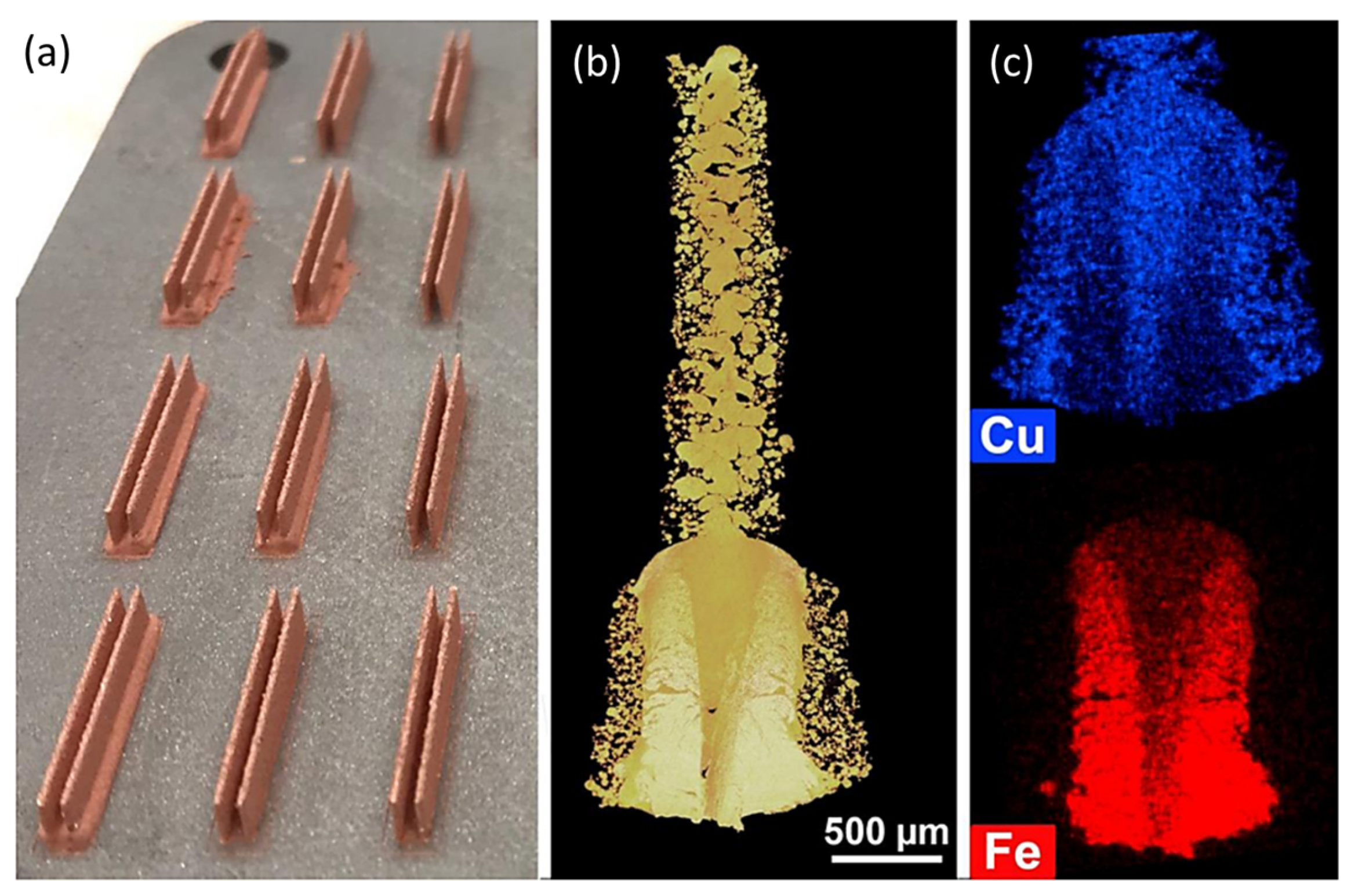
Figure 4. (a) Free-standing pure copper thin walls fabricated via NIR L-PBF at various laser powers, scan speeds, and layer thicknesses, (b) cross-section of thin walls illustrating bulging at the base, and (c) EDX analysis of cross-section highlighting iron contamination at the base causing the bulging.
Additionally, Silbernagel et al. [19] also investigated the changes in the chemical composition of the pure copper meltpool when a steel substrate is used. Due to the low thermal conductivity of steel, it has now become a common approach to use steel substrates instead of copper substrates to prevent rapid heat loss from the meltpool during the L-PBF of pure copper, especially during the critical initial layers to prevent delamination. Here, the authors found through EDX analysis that a considerable amount of iron had diffused into the meltpool for the first 1.5 mm in the vertical build direction, which resulted in a physical bulging of the thin walls (see Figure 4b,c). Nonetheless, at higher build heights, the copper concentration returned to near 100% purity levels and any previously iron-contaminated layers did not remelt, which prevented further diffusion of iron along the build direction. Physically, this is marked by a notable decrease in wall thickness past the iron-contaminated zone.
To overcome the key challenge of meltpool heat loss encountered by long-pulse or continuous wavelength lasers that are common to many L-PBF printers, Kaden et al. first explored the use of ultrashort pulse (USP) femtosecond lasers in 2017 [20]. The authors theorised that the extremely short interaction times between the USP laser and the powder feedstock would drastically minimise heat loss from the meltpool during laser exposure, and thus be able to retain a greater amount of energy for the complete melting and fusion to occur. Furthermore, the confinement of the active heating zone to the immediate vicinity of the illuminated area would also enhance the precision and resolution of filigree copper geometries. As a result, the authors were able to fabricate homogenous thin-wall structures of approximately 100 µm in wall thickness with a height-to-width aspect ratio of 15:1 (see Figure 5a). However, incomplete fusion was still clearly observable through scanning electron microscopy (see Figure 5b). The authors attributed the lack of densification to a non-optimal ratio of beam spot size to particle diameter, by reasoning that since only particles that underwent direct laser exposure would melt and fuse together to form a bead, using particles and beam spot diameter of the same size order (35 µm) would prevent the consolidation and fusion of adjacent particles into the meltpool during exposure.
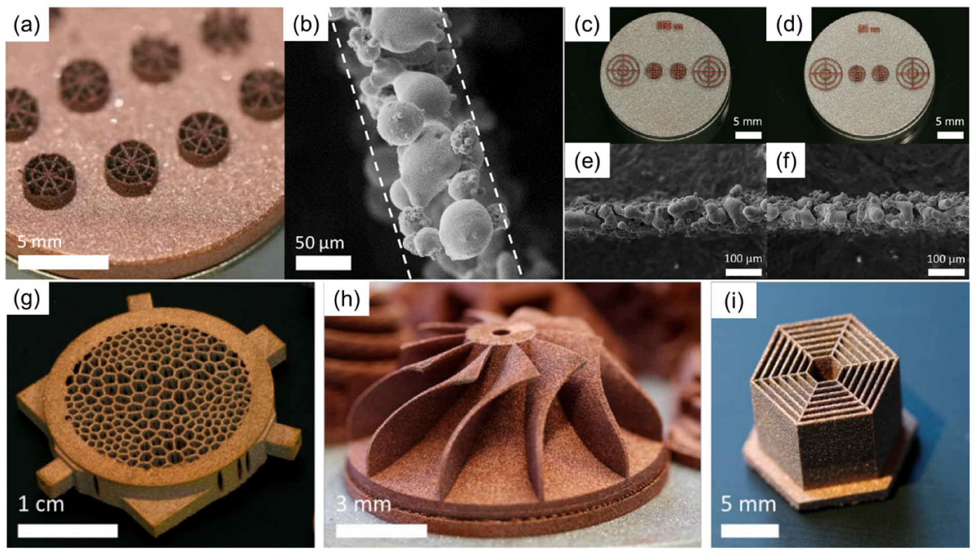
Figure 5. (a) Pure copper thin-wall structures fabricated using ultrashort pulse L-PBF, (b) SEM image of thin-wall structure displaying wall thickness of 100 µm and homogeneous high porosity, (c,d) pure copper thin-wall structures fabricated using ultrashort pulse L-PBF at 1030 nm (NIR) and 515 nm (green) wavelengths, (e,f) corresponding SEM images to (c,d) showing the highly similar structures produced, (g) topology-optimised structure for a lightweight mirror mount, (h) turbine wheel with highly inclined overhanging thin fins not requiring support structures, and (i) thin-wall structure with 100 µm wall thickness and extremely high aspect ratio of 70:1.
In a later study [21], Kaden et al. compared the performances of USP lasers at 1030 nm (NIR) and 515 nm (green) wavelengths in fabricating thin-wall structures (see Figure 5c,d). While the beam spot size of both lasers was similar, hardware restrictions limited the power output of the green laser to half that of the NIR laser. In comparison to the NIR laser, a smaller layer thickness of 15 µm instead of 30 µm was used for the green laser, as well as a smaller particle size of 10 µm instead of 25 µm. The authors observed that the thin walls produced by both lasers yielded highly similar geometrical resolutions and morphologies, with an average wall thickness below 100 µm (see Figure 5e,f). This suggested that the effective energy absorbed by the illuminated copper feedstock at 515 nm is approximately double that of 1030 nm. Regardless of laser wavelength, however, full densification could still not be achieved. Nonetheless, the power output produced by the USP lasers at 11 W (green) and 24 W (NIR) needs to be taken into consideration, which is extremely low compared to the 1 kW laser systems available today. Moreover, the ability of the copper feedstock powder to even melt and fuse together at such low levels of output in the first place is evidence of the latent potential of USP lasers. For example, in further investigations with the green USP laser for actual engineering components, Kaden et al. [22] were able to achieve filigree copper geometries such as complex organic structures (Figure 5g), reduce the strain and support structures for thin overhanging regions (Figure 5h), and produce thin-wall structures with extremely high aspect ratios of 70:1 (Figure 5i).
In another attempt to improve densification of thin-wall structures, Ma et al. [23] investigated the influence of using higher NIR laser powers of up to 500 W for various scan speeds and hatching distances on the relative density, surface roughness, and wall thickness of thin-wall copper flanged samples (see Figure 6a,b).

Figure 6. (a) Influence of using higher NIR laser powers up to 500 W for various scan speeds and hatching distances on relative density, surface roughness, and wall thickness, (b) resulting copper flanges fabricated from process parameters shown in (a), (c) main effect plots for laser power, scan speed, and hatching distance on relative density, (d) schematic of linear scanning and circular scanning exposure strategies, and (e) comparison of wall thickness, surface roughness, and relative density for linear and circular scanning exposure strategies.
At higher laser powers above 400 W, the authors were able to consistently obtain relative densities of the thin walls above 99%, as shown in Figure 6a. In fact, unlike the insensitivity of the meltpool to changes in laser outputs below 200 W [19], the authors found that when the laser output was increased from 200 W to 300 W, the relative density could be significantly improved to nearly full density levels, regardless of the scan speeds or hatching distance used (see Figure 6c). Hence, it seems that a minimum output of 300 W would be required for NIR lasers before full densification could be obtained. However, there is a trade-off in dimensional accuracy when higher laser powers are used, with physical wall thickness ranging from two to four times that of the digital model. While the authors could compensate for the additional material by simply reducing wall thickness in the digital model to 50 µm to achieve the desired value of 200 µm for the physical part, it is noted that such an approach could be challenging to implement for complex finned structures of varying cross-sectional areas such as in topology-optimised heat sink geometries. The authors also found that the exposure strategy played an important role in determining the wall thickness and surface roughness of the parts. In general, implementing a circular scanning strategy that conformed to the cylindrical geometry of the parts instead of a generic linear scanning strategy (see Figure 6d) produced more accurate wall thicknesses and lower surface roughness (see Figure 6e). Here, further developments in customised geometry-dependent exposure strategies for filigree geometries beyond basic primitive shapes are highly anticipated due to the potential scale of improvements that can be unlocked with this technique.
So far, the fabrication of pure copper thin-wall geometries via typical NIR lasers with an output below 200 W does not seem capable for obtaining fully dense or near fully dense structures. This is further affirmed through the work of Jadhav et al. [24], who used an empirically validated analytical model for the L-PBF processing characteristics of pure copper at laser powers ranging from 200 W to 500 W with different scan speeds (see Figure 7a).
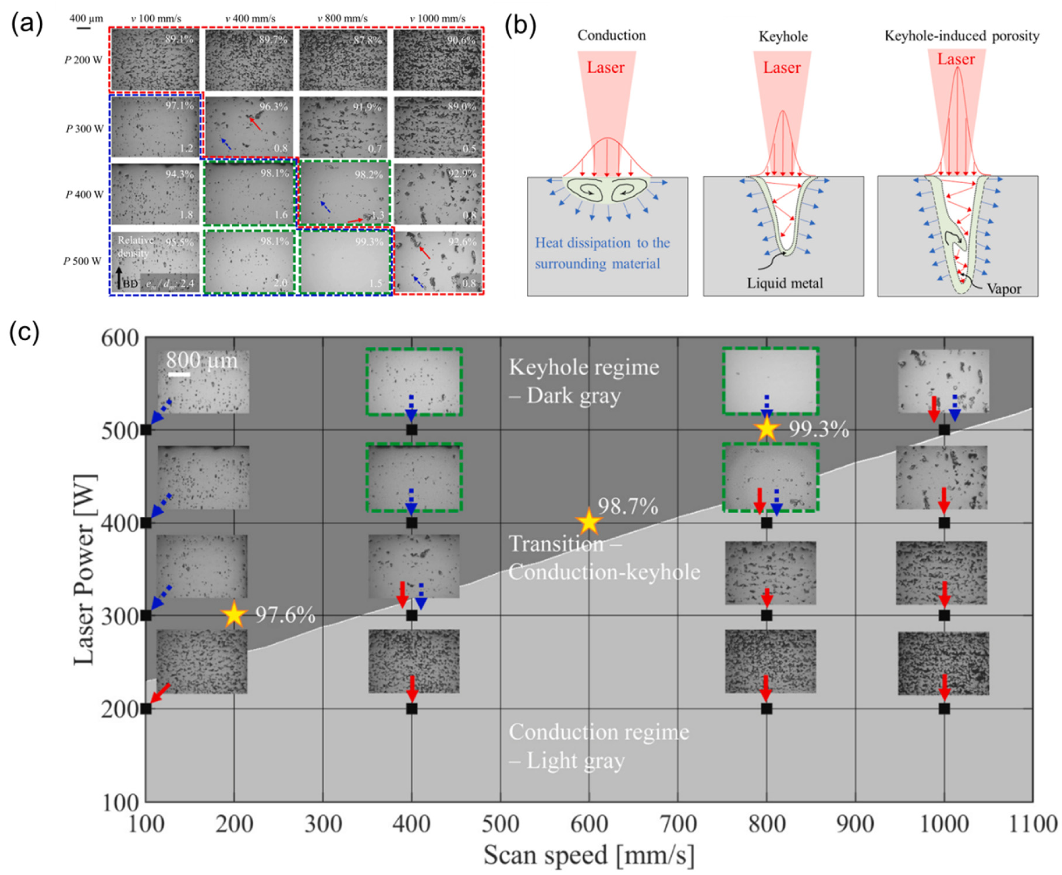
Figure 7. (a) Porosity analysis images of bulk copper specimens fabricated using NIR L-PBF between 200 W and 500 W for various scan speeds, with green dotted outline representing ideal keyhole regime with good fusion, blue dotted outline representing keyhole-induced porosity regime, and red outline representing lack-of-fusion conduction regime, (b) schematics of conduction, keyhole, and keyhole-induced porosity regimes in L-PBF of pure copper, (c) mapping of keyhole regime, conduction regime, and transition zone between regimes to laser power and scan speed.
While no thin-wall structures were investigated, the authors were able to obtain relative densities exceeding 99% for bulk pure copper specimens using a 1080 nm wavelength laser with beam spot size of 37.5 µm, laser power of 500 W, and range of scan speeds corresponding to a volumetric energy density window of 230 to 310 J/mm3. A standard L-PBF powder feedstock size of 25–60 µm was used.
Perhaps of greater interest is that the analytical model categorised the L-PBF processing of pure copper into two different processing windows—the conduction regime and keyhole regime (inclusive of keyhole-induced porosity, see Figure 7b). The authors found that for highly reflective materials such as copper to be fully densified using NIR lasers, the processing window needs to occur in the keyhole regime. The formation of keyholes is the critical factor that enables full densification to occur, since effective laser absorption is exponentially increased by the presence of multiple internal reflections of the laser within the keyhole, as shown in Figure 7b. However, the keyhole also needs to be stabilised through an optimal processing window—in essence, for copper, since the bottom half of the keyhole absorbs approximately four times the amount of laser energy as the top half of the keyhole [25], it is more likely to remain in the molten state while the top half solidifies earlier [26]. This will result in trapped or keyhole-induced porosity within the material, which is exacerbated by introducing overly large amounts of volumetric energy density. Conversely, too little volumetric energy density places the L-PBF of copper into the conduction regime, in which most of the laser energy is reflected or dissipated away instead of being absorbed by the meltpool. Hence, for typical copper feedstock sizes at NIR wavelengths, this corresponds to the narrow processing window of 230 to 310 J/mm3 (see Figure 7c).
However, the authors also concluded that it is the formation of stable keyhole features, rather than the laser power per se, that enables the production of bulk solid copper at full densities. Hence, it follows that as long as optimal keyholes can be formed, it will still be possible to obtain the full densification at laser powers below 500 W by optimising other key process variables in L-PBF such as particle size, baseplate material, and platform heating, modifying the surface of the copper feedstock for higher optical absorption of NIR (1060 nm) wavelength laser energy, or using green (515 nm) or blue (450 nm) wavelength lasers which have inherently better absorptivity by non-modified copper powder particles (see Figure 8).
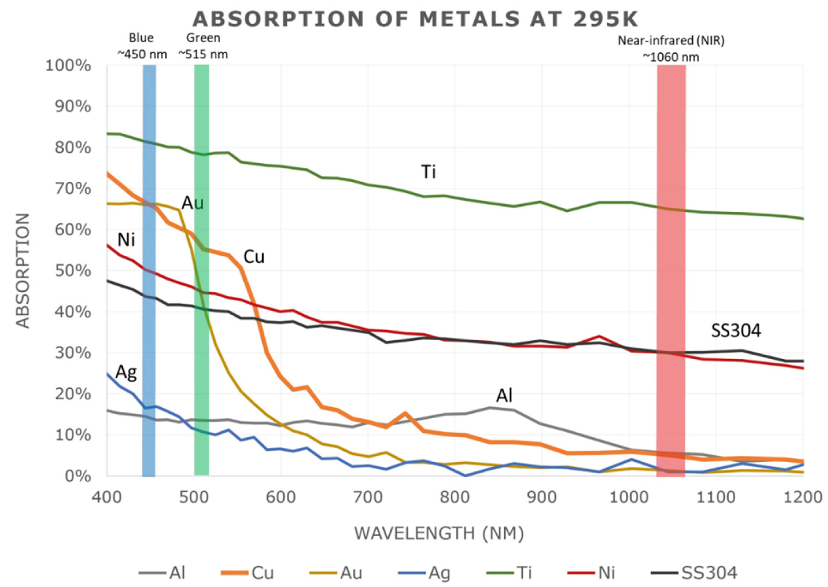
Figure 8. Absorption of metals at different irradiation wavelengths.
Such approaches were indeed used by Qu et al. [27], who were able to obtain pure copper bulk components with a relative density of 99.6% at 200 W of NIR laser output from a high precision L-PBF system with a small beam spot size of 25 µm, fine power particles between 5 µm and 25 µm, a small layer thickness of 10 µm, and 316 L stainless steel substrate. The authors were also able to achieve an electrical conductivity of 96% IACS after the heat treatment of the components, which suggests an ideal thermal conductivity that is near to the theoretical limits of copper. Thin-wall structures using an exposure strategy of single-line scan tracks (see Figure 9a,b) were also fabricated over a range of laser powers and scan speeds (see Figure 9c).
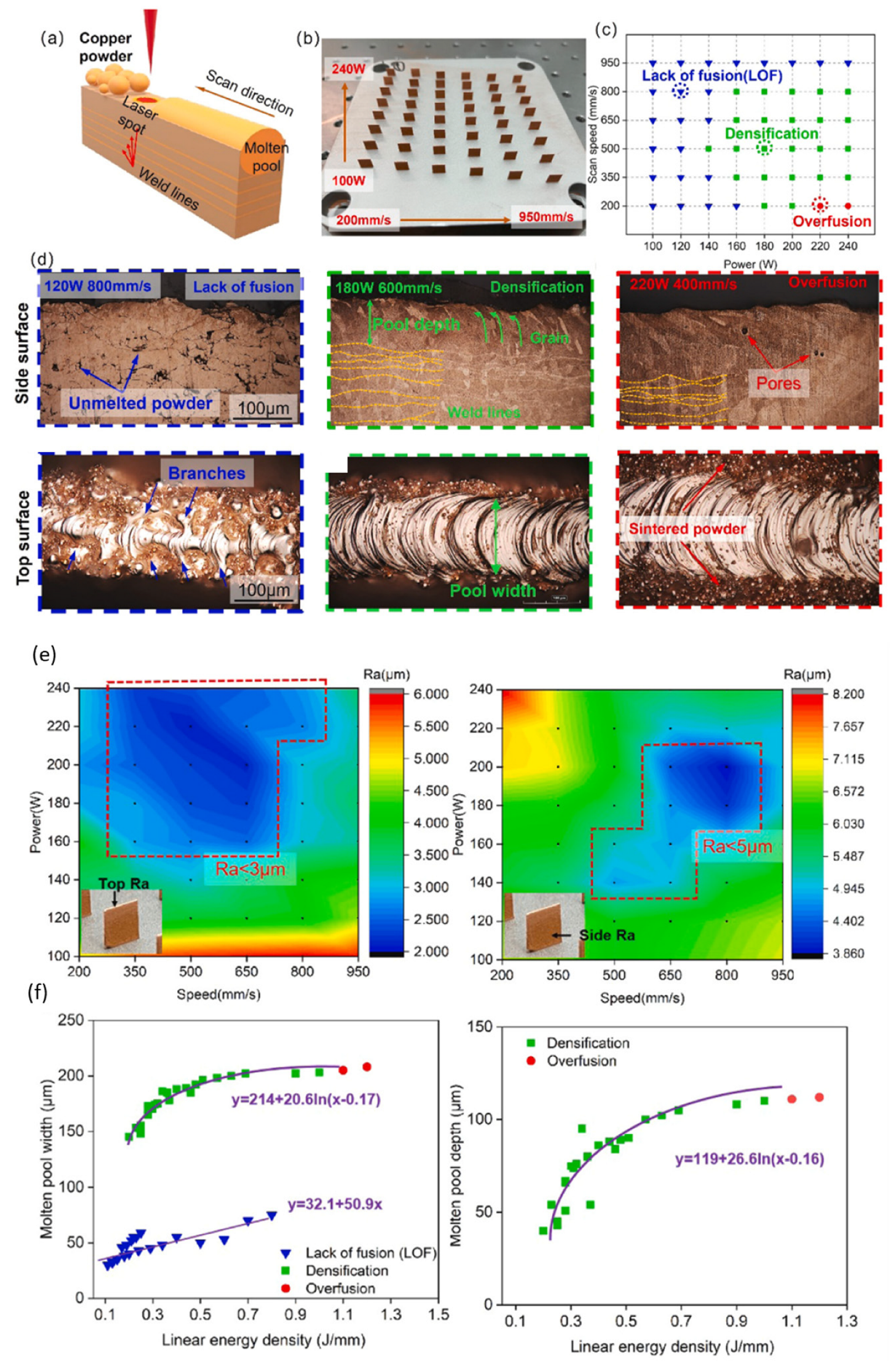
Figure 9. (a) Schematic of single-line exposure strategy used to fabricate thin walls, (b) free-standing thin walls fabricated using a bespoke high precision NIR L-PBF at various laser powers and scan speeds, (c) processing windows for lack of fusion, densification, and overfusion, (d) close up of side and top surfaces of thin walls for different processing windows, as indicated, (e) top and side surface roughness of thin walls for different processing windows, and (f) meltpool width and depth for different processing windows.
The authors observed processing characteristics similar to what had been reported by Jadhav et al. [24]—lack of fusion, densification, and overfusion (see Figure 9c,d), Nonetheless, the inherently high precision of the printer and material feedstock system lend themselves well to producing high-density thin walls with low surface roughness between Ra 3 and 5 µm (see Figure 9e), and wall thicknesses as low as 150 µm. The meltpool depth was also found to be well-controlled and ranging between 50 and 100 µm depending on the process parameters used (see Figure 9f), which is important in three-dimensional shell-based triply periodic minimal surface lattice structures consisting of vertical thin walls, as well as horizontal thin ‘floors’ and ‘ceilings’. Overall, the geometrical quality, surface roughness, and material properties of the filigree components fabricated by Qu et al. are highly favourable for advanced thermal management devices.
Recently, continuous short-wavelength lasers of 515 nm (green) and 450 nm (blue) have begun to emerge for use in L-PBF systems, due to the aforementioned higher energy pure copper absorptivity of these wavelengths. Contrary to NIR lasers, the current optical hardware capabilities of these short-wavelength lasers appear to have a minimum beam spot size of 200 µm [28][29][30][31][32][33], which results in an illuminated area that is up to six times as large as that of a typical 80 µm beam spot size for NIR lasers. In fact, even for the same beam spot size and laser process parameters over a range of different scan speeds, Hori et al. [29] observed that the copper meltpool bead size for a blue laser was consistently two to four times larger than that of a NIR laser (see Figure 10).
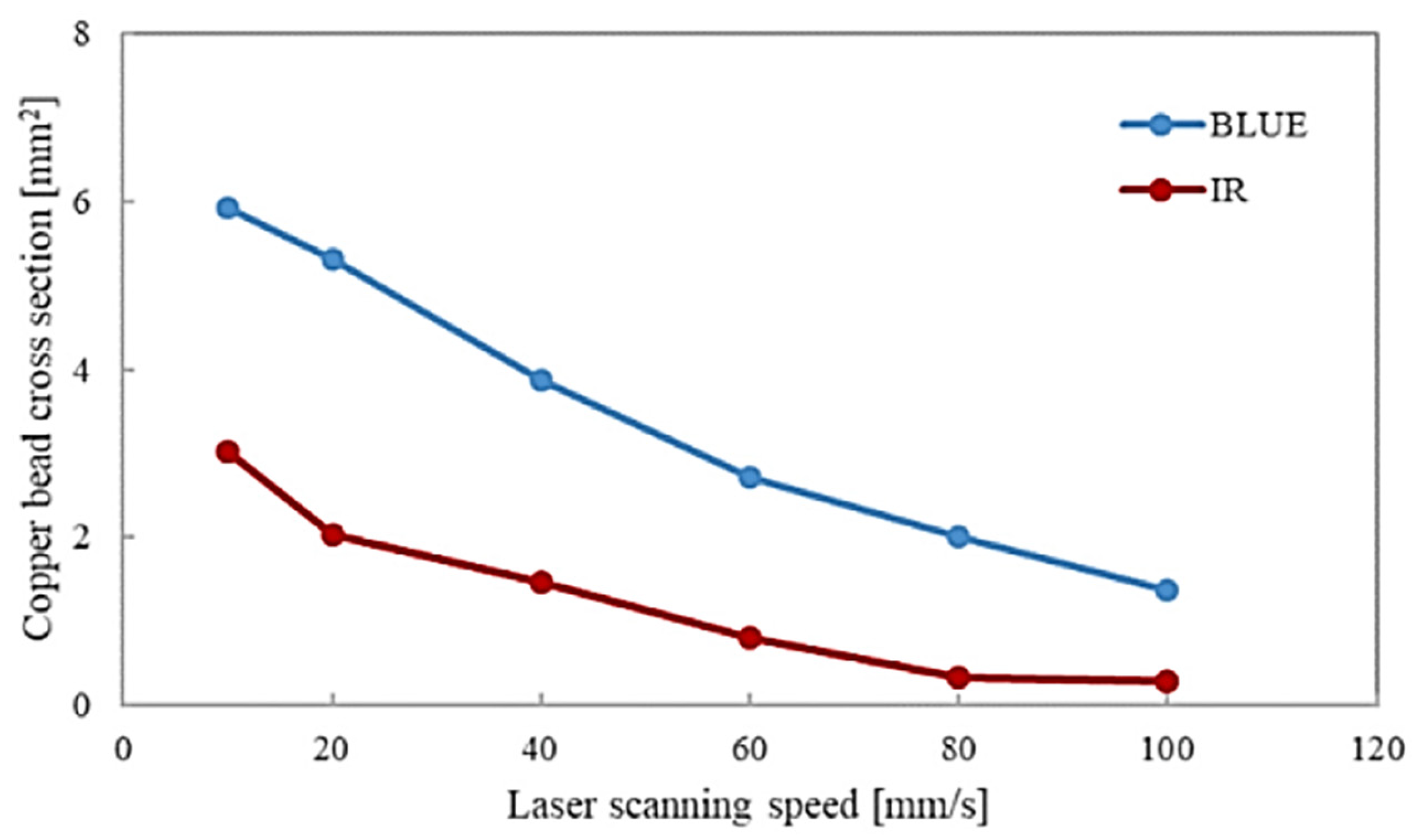
Figure 10. Comparison of meltpool bead size between NIR and short-wavelength blue lasers with same beam spot size at different scan speeds.
Horn et al. [31] fabricated thin-wall structures at different inclination angles of 90° (vertical), 60°, and 30° (see Figure 11a) using a continuous wavelength green laser with a beam spot size of 200 µm and maximum power of 500 W. The authors observed that while highly dense core regions of the thin walls could be achieved, an enveloping porous and branch-like structure of solidified melt beads known as ‘drips’ was also concurrently formed (see Figure 11b), regardless of laser power, scan speed, or exposure strategy used. While the extent of the drips could be reduced at more horizontal inclination angles, they could not be fully removed, and inadvertently resulted in higher surface roughness that is accompanied by an increase in wall thickness of 22% to 83% of the dense core region (see Figure 11c).
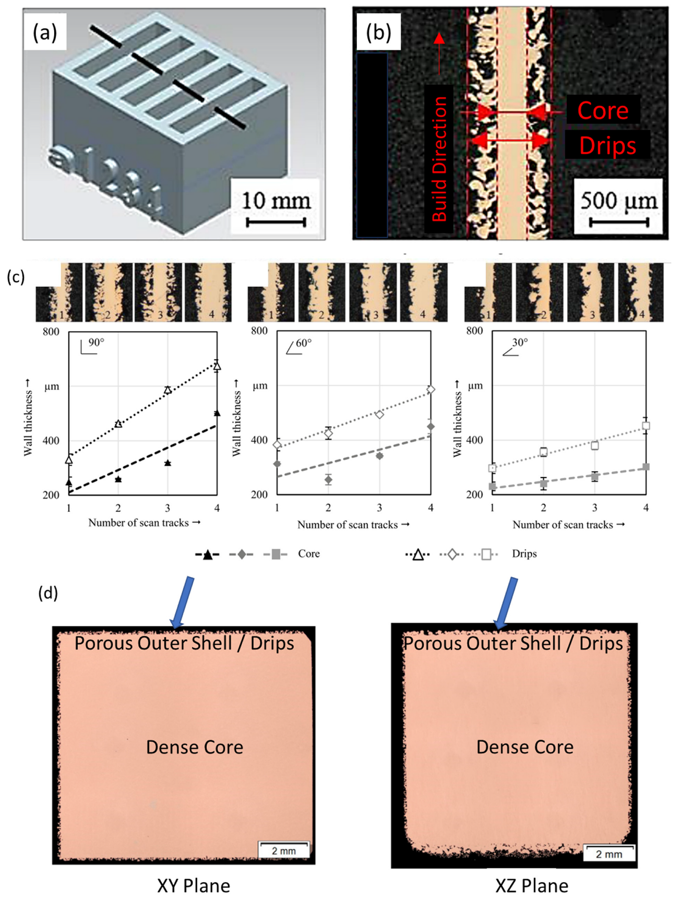
Figure 11. (a) Design of thin-wall specimen coupons for fabrication with a continuous wavelength green laser, (b) cross-section of thin walls consisting of a dense core region with porous branch-like structures of solidified melt beads, (c) wall thickness of thin walls fabricated using different number of scan tracks at print angles of 90° (vertical), 60°, and 30°, and (d) similar dense core/porous outer shell phenomena is observed in another study when green lasers are used.
Horn et al. further noted that the presence of drips were also observed in another study on the L-PBF of pure copper using a green laser [28], however, since they only occurred around the borders of the bulk material due to the remelting of the core regions via overlapping meltpool hatching, fully dense and defect-free parts could still be obtained and the effects of the drips on bulk geometries (see Figure 11e) were considered less significant compared to filigree geometries. In the context of thin-wall structures for thermal management devices, however, the reviewed literature suggests that the current hardware capabilities of short-wavelength lasers are still not as refined as medium power (≥400 W) NIR lasers at producing high-resolution geometries with smooth surfaces for rapid heat transfer and minimal flow losses (see Figure 12).
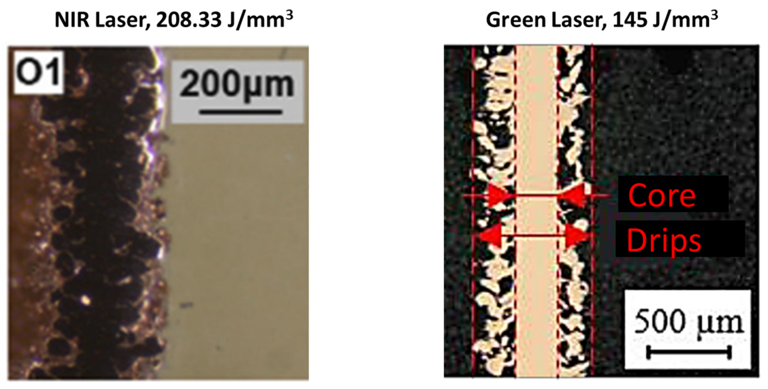
Figure 12. Comparison of thin-wall fabrication capabilities of NIR lasers and green lasers.
As the scientific community continues to make progress in beam-based AM techniques to process pure copper filigree geometries, another promising group of techniques that has begun to emerge is sinter-based AM. Sinter-based AM refers to any AM process that involves a two-stage shape and sinter approach in the fabrication of 3D components. With reference to Figure 13a, the first stage involves the shaping of parts into the desired geometry either via the extrusion of a metal–polymer paste or filament through a nozzle (material extrusion), via the selective jetting of a polymer binder into the power bed (binder jetting), or via the selective curing of a metal–polymer slurry using light (vat photopolymerisation). At this stage, regardless of how the parts have been shaped, they would all consist of metal particles that are only temporarily bonded together by the polymer adhesives. In the second stage, the parts are sintered in a furnace to remove the polymer binders and form metallurgical bonds between the particles for further densification. Thus, sinter-based AM inherently avoids the poor absorptivity of copper particles to laser irradiation by removing the need for a laser to melt and fuse the particles together in the first place. Optimal selection of polymer binders and process parameters for debinding and sintering, however, will be critical to obtaining dense, dimensionally accurate, and residue-free copper parts.
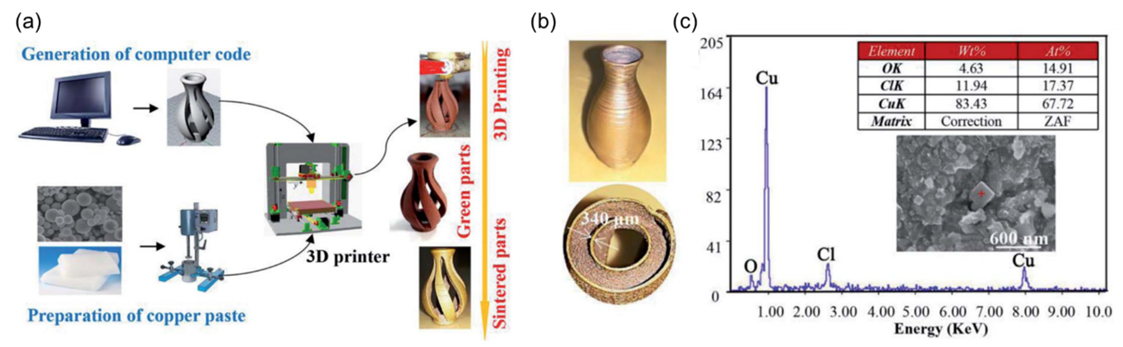
Figure 13. (a) Workflow of paste material extrusion method, (b) vase-like geometry formed using material extrusion with smooth walls of 340 µm wall thickness, and (c) EDX analysis indicates no carbon residue after pyrolysis, but some amount of oxygen is detected.
For example, Yan et al. [34] utilised a paste material extrusion method to form a vase-like thin-wall cylinder (see Figure 13a) in 2018. The paste consisted of 1 µm copper powder particles (purity > 99.5%) mixed with paraffin wax at a powder to wax mass ratio of 10:1. After sintering, the authors were able to obtain thin-wall structures with a relative density of 90.4%, hardness of 80 HV, and a wall thickness of 340 µm that appears visually smooth (see Figure 13b). SEM analysis indicated high metallurgical bonding, while EDX analysis revealed that no residual carbon from binder pyrolysis was retained in the material (see Figure 13c). However, the oxygen content was around 5% by mass, which can be detrimental to the conductivity of pure copper. It is likely that the oxygen pick-up could have originated from the paste preparation in an exposed environment at elevated temperatures of 70–80 °C, during which slight oxidation of the copper particles can occur due to their high surface area to volume ratio. Further validation is required in this area. Regardless, the proper handling of specimens in sinter-based AM is required due to the lack of an inert process chamber that is inherent to beam-based powder bed fusion processes.
One of the most exciting and modern developments in the sinter-based AM of pure copper is the digital light processing (vat photopolymerisation) of a metal–polymer slurry, in which the extremely high resolution of digital light processing (see Figure 14a) in combination with a mature sintering process rooted in conventional metal injection moulding results in thin-wall structures of high density (95% bulk density), electrical conductivity (92% IACS), and thermal conductivity (92% copper standard) at just 100 µm thick [35] (see Figure 14b). This technique is currently exclusive to one commercial manufacturer, however, and future developments in this space by other AM manufacturers is anticipated.
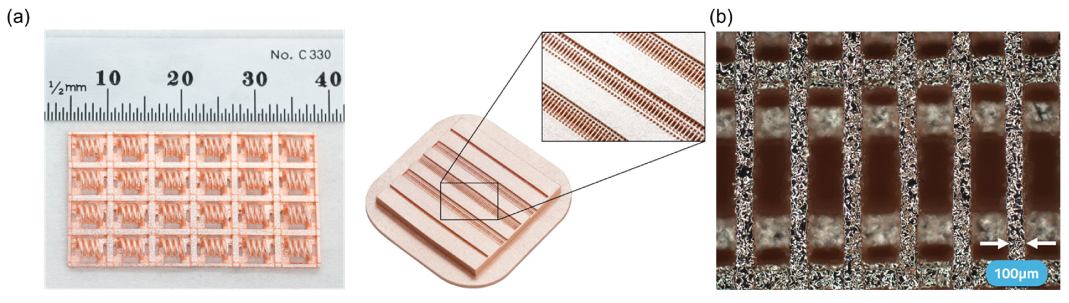
Figure 14. (a) Extremely high resolution of small components fabricated using digital light processing (vat photopolymerisation) of a copper slurry, and (b) wall thickness as low as 100 µm with visually high geometrical stability and smooth surfaces.
2.2. Lattice Structures
While the thin walls reviewed so far are predominantly vertically orientated features that are targeted for use as fins of single-fluid domain heat sinks, the intertwining passageways in heat exchangers with two or more fluid domains necessitate a more elaborate 3D volumetric structure in the form of TPMS shell-based lattice structures.
By definition, TPMS are minimal surfaces that recur periodically in three independent directions, e.g., the X, Y, and Z cartesian axes [36]. Hence, TPMS lattices can be visualised as repeating unit shells that are formed by thin walls, thin ‘floors’, and thin ‘ceilings’ with smooth curvatures. This makes TPMS a more challenging geometry to produce than solely vertical thin walls for beam-based AM due to the addition of overhangs and curved surfaces that are susceptible to over-heating from excessive meltpool depth penetration (Figure 15a) and the staircase effect (Figure 15b). Nevertheless, the principles behind the AM fabrication of thin-wall structures are still applicable for TPMS lattices.

Figure 15. (a) Increased deformation and overheating at high inclination angles for overhangs, and (b) staircase effect of inclined or curved surfaces.
For example, Qu et al. [27] fabricated N14 and primitive-type TPMS lattice structures using their self-developed high-precision NIR L-PBF system (see Figure 16a). Optical microscopy analysis of the top surface cross-sectional area indicated a wall thickness of 100 µm with a dense and pore-free microstructure (see Figure 16b). Conversely, the side surface cross-sectional area exhibited a significantly higher wall thickness of 149 µm (see Figure 16c) due to the staircase effect. Surface roughness (see Figure 16d) was also highly dependent on build orientation and increased in order of top-facing (Ra 3.3 µm), side-facing (Ra 14.8 µm), and bottom-facing overhanging surfaces (Ra 19.2 µm). This is because at increasingly horizontal overhangs, the meltpool depth can penetrate through the overhanging region, which results in the remelting of the solidified layers and partial fusion of powder particles to the underlying surface (see Figure 16e).
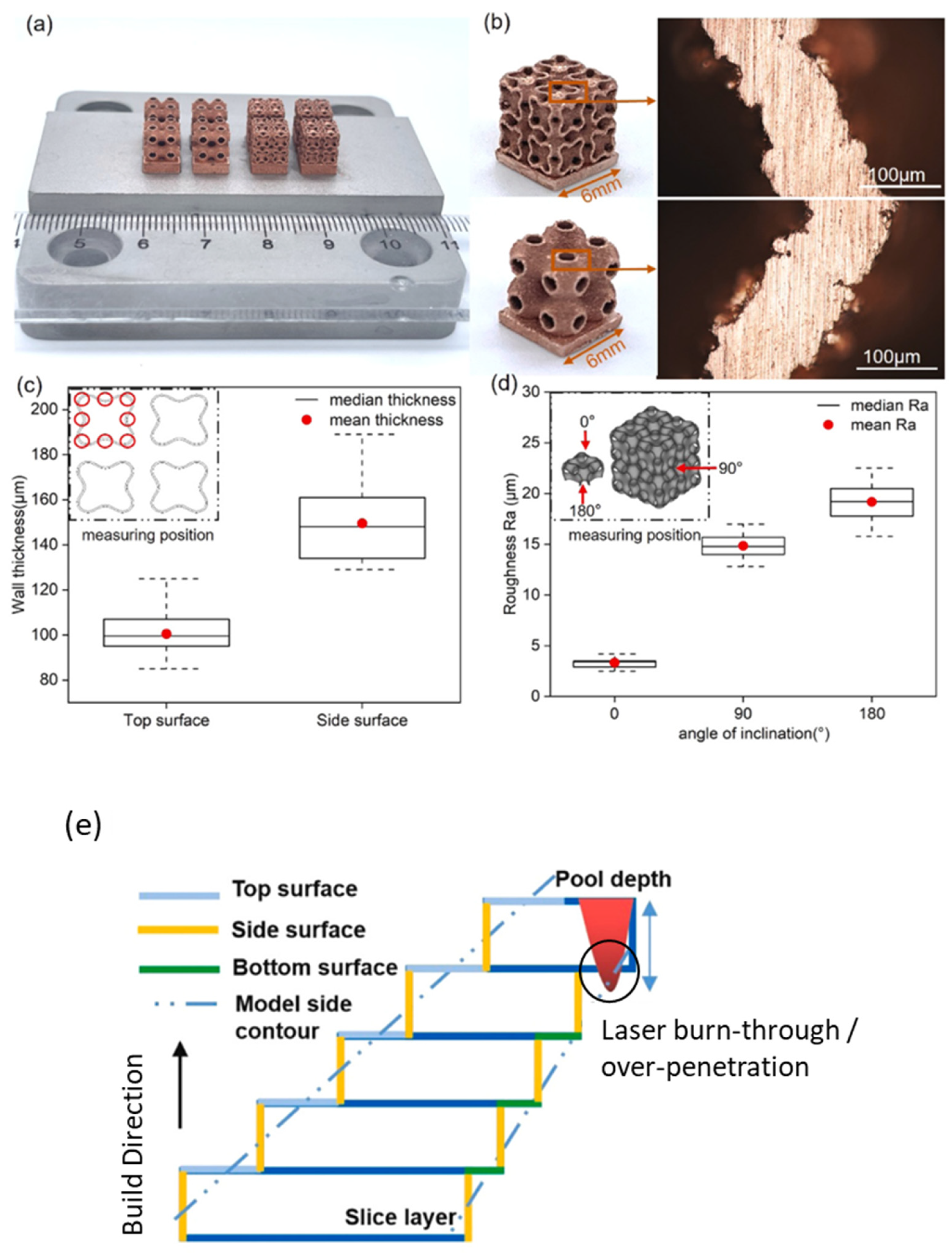
Figure 16. (a) N14 and primitive-type lattice structures fabricated using a high precision NIR L-PBF printer, (b) cross-sectional area of vertical lattice wall shows good densification, smooth surfaces, and a thickness of 100 µm (c) comparison of wall thickness for top and side surfaces, (d) comparison of surface roughness for top and side surfaces, and (e) schematic illustrating laser burn-through and over-penetration for highly inclined surfaces.
In contrast to NIR lasers, lattice structures fabricated using blue and green lasers face challenges with minimum feature size and smooth surfaces [37][38], which is a similar outcome from the thin-wall geometries shown earlier. Visual examples of lattices that were fabricated using blue and green short-wavelength lasers are shown in Figure 17.
Figure 17. Larger minimum unit cell size, lower resolution, and rougher surfaces in lattice structures produced using a (a) blue laser and (b) green laser in L-PBF.
Nevertheless, NIR lasers are not without their challenges. As mentioned earlier, Jadhav et al. [24] reported that the optimal processing window for dense and well-formed pure copper structures using NIR lasers can occur only in a small range within the keyhole regime. This is further validated by Alphonso et al. [39], who conducted a comparison study of both green and NIR lasers using a benchmark artifact. Through numerical modelling and experimental verification, the authors determined that while both conduction and keyhole regimes are feasible processing windows for green lasers, only the keyhole melting regime is practical for NIR lasers. Hence, without fine tuning the process parameters for specific geometries, the use of NIR lasers in lattice structures can also result in unstable meltpools and distorted geometries [39] (see Figure 18).

Figure 18. The narrow processing windows of pure copper for NIR lasers in L-PBF can result in unstable meltpools and distorted geometry (red outline) compared to green lasers with larger processing windows.
In terms of the sinter-based AM of pure copper lattice structures, the technique that appears to have made the most demonstratable progress is vat photopolymerisation. Just like for thin-wall structures, the resolution, surface roughness, and surface homogeneity for TPMS lattice structures appear outstanding with this technique (see Figure 19). An improvement in isotropic properties compared to beam-based AM is also expected, due to increased grain texture homogeneity from the sintering process instead of an elongated grain structure that is characteristic of beam-based AM techniques [38]. This is critical to the thermal and electrical conductivity of pure copper since grain boundaries, especially low-angle grain boundaries with misorientation angles between 14° and 18°, induce dislocation and strain in the crystal lattice, which inhibit electron mobility and increase resistance [40]. Furthermore, the nodes of the lattice structures fabricated using beam-based AM typically contain high residual stresses due to repeated melting and solidification cycles [38].

Figure 19. Complex triply periodic minimal surface lattice structures with high resolution and smooth homogeneous surfaces using digital light processing (vat photopolymerisation).
References
- nTop Heat Exchanger Design with Additive Manufacturing. Available online: https://www.ntop.com/resources/blog/heat-exchanger-design-with-additive-manufacturing/ (accessed on 24 May 2023).
- EOS 3D Printing Metal Materials. Available online: https://www.eos.info/en/3d-printing-materials/metals (accessed on 24 May 2023).
- SLM Solutions SLM® Metal Powder & Material Parameters. Available online: https://www.slm-solutions.com/products-and-solutions/powders/ (accessed on 24 May 2023).
- Velo3D Materials. Available online: https://velo3d.com/products/#materials (accessed on 24 May 2023).
- Desktop Metal Materials for All of Your Applications. Available online: https://www.desktopmetal.com/materials (accessed on 24 May 2023).
- Markforged 3D Printing Materials. Available online: https://markforged.com/materials (accessed on 24 May 2023).
- EOS EOS Copper CuCP for AMCM M 290 1 KW. Available online: https://www.eos.info/03_system-related-assets/material-related-contents/metal-materials-and-examples/metal-material-datasheet/copper/material_datasheet_eos-_copper_cucp_en_web.pdf (accessed on 16 March 2023).
- TRUMPF TruPrint 1000 Green Edition. Available online: https://www.trumpf.com/filestorage/TRUMPF_Master/Products/Machines_and_Systems/02_Brochures/TRUMPF-TruPrint-1000-Green-Edition-flyer-EN.pdf (accessed on 16 March 2023).
- TRUMPF TruPrint 5000 Green Edition. Available online: https://www.trumpf.com/filestorage/TRUMPF_Master/Products/Machines_and_Systems/02_Brochures/TRUMPF-TruPrint5000-Green-Edition-flyer-EN.pdf (accessed on 16 March 2023).
- Engler, S.; Ramsayer, R.; Poprawe, R. Process Studies on Laser Welding of Copper with Brilliant Green and Infrared Lasers. Phys. Procedia 2011, 12, 339–346.
- Jadhav, S.D.; Dadbakhsh, S.; Goossens, L.; Kruth, J.-P.; Van Humbeeck, J.; Vanmeensel, K. Influence of Selective Laser Melting Process Parameters on Texture Evolution in Pure Copper. J. Mater. Process. Technol. 2019, 270, 47–58.
- Singer, F.; Deisenroth, D.C.; Hymas, D.M.; Ohadi, M.M. Additively Manufactured Copper Components and Composite Structures for Thermal Management Applications. In Proceedings of the 2017 16th IEEE Intersociety Conference on Thermal and Thermomechanical Phenomena in Electronic Systems (ITherm), Orlando, FL, USA, 30 May–2 June 2017; IEEE: Orlando, FL, USA; pp. 174–183.
- Romano, T.; Vedani, M. Additive Manufacturing of Pure Copper: Technologies and Applications. In Copper—From the Mineral to the Final Application; IntechOpen: London, UK, 2022.
- Jiang, Q.; Zhang, P.; Yu, Z.; Shi, H.; Wu, D.; Yan, H.; Ye, X.; Lu, Q.; Tian, Y. A Review on Additive Manufacturing of Pure Copper. Coatings 2021, 11, 740.
- Roccetti Campagnoli, M.; Galati, M.; Saboori, A. On the Processability of Copper Components via Powder-Based Additive Manufacturing Processes: Potentials, Challenges and Feasible Solutions. J. Manuf. Process. 2021, 72, 320–337.
- Tran, T.Q.; Chinnappan, A.; Lee, J.K.Y.; Loc, N.H.; Tran, L.T.; Wang, G.; Kumar, V.V.; Jayathilaka, W.A.D.M.; Ji, D.; Doddamani, M.; et al. 3D Printing of Highly Pure Copper. Metals 2019, 9, 756.
- Guan, J.; Zhang, X.; Jiang, Y.; Yan, Y. Insights into Fabrication Mechanism of Pure Copper Thin Wall Components by Selective Infrared Laser Melting. Rapid Prototyp. J. 2019, 25, 1388–1397.
- Matthews, M.J.; Guss, G.; Khairallah, S.A.; Rubenchik, A.M.; Depond, P.J.; King, W.E. Denudation of Metal Powder Layers in Laser Powder Bed Fusion Processes. Acta Mater. 2016, 114, 33–42.
- Silbernagel, C.; Gargalis, L.; Ashcroft, I.; Hague, R.; Galea, M.; Dickens, P. Electrical Resistivity of Pure Copper Processed by Medium-Powered Laser Powder Bed Fusion Additive Manufacturing for Use in Electromagnetic Applications. Addit. Manuf. 2019, 29, 100831.
- Kaden, L.; Matthäus, G.; Ullsperger, T.; Engelhardt, H.; Rettenmayr, M.; Tünnermann, A.; Nolte, S. Selective Laser Melting of Copper Using Ultrashort Laser Pulses. Appl. Phys. A Mater. Sci. Process. 2017, 123, 596.
- Kaden, L.; Seyfarth, B.; Ullsperger, T.; Matthäus, G.; Nolte, S. Selective Laser Melting of Copper Using Ultrashort Laser Pulses at Different Wavelengths. In Laser 3D Manufacturing V; Helvajian, H., Piqué, A., Gu, B., Eds.; SPIE: Bellingham, WA, USA, 2018; Volume 1052312, p. 41.
- Kaden, L.; Matthäus, G.; Ramm, R.; Ullsperger, T.; Seyfarth, B.; Nolte, S. Additive Manufacturing of Pure Copper Using Ultrashort Laser Pulses. In Laser 3D Manufacturing VI; Helvajian, H., Gu, B., Chen, H., Eds.; SPIE: Bellingham, WA, USA, 2019; p. 12.
- Ma, Z.X.; Ning, J.; Yu, B.; Zhang, L.J.; Fan, J.H.; Yuan, L.G. Effects of Process Parameters and Scanning Patterns on Quality of Thin-Walled Copper Flanges Manufactured by Selective Laser Melting. J. Manuf. Process. 2021, 72, 419–430.
- Jadhav, S.D.; Goossens, L.R.; Kinds, Y.; Van Hooreweder, B.; Vanmeensel, K. Laser-Based Powder Bed Fusion Additive Manufacturing of Pure Copper. Addit. Manuf. 2021, 42, 101990.
- Zhang, L.-J.; Zhang, G.-F.; Ning, J.; Zhang, X.-J.; Zhang, J.-X. Microstructure and Properties of the Laser Butt Welded 1.5-Mm Thick T2 Copper Joint Achieved at High Welding Speed. Mater. Des. 2015, 88, 720–736.
- Bayat, M.; Thanki, A.; Mohanty, S.; Witvrouw, A.; Yang, S.; Thorborg, J.; Tiedje, N.S.; Hattel, J.H. Keyhole-Induced Porosities in Laser-Based Powder Bed Fusion (L-PBF) of Ti6Al4V: High-Fidelity Modelling and Experimental Validation. Addit. Manuf. 2019, 30, 100835.
- Qu, S.; Ding, J.; Fu, J.; Fu, M.; Zhang, B.; Song, X. High-Precision Laser Powder Bed Fusion Processing of Pure Copper. Addit. Manuf. 2021, 48, 102417.
- Gruber, S.; Stepien, L.; López, E.; Brueckner, F.; Leyens, C. Physical and Geometrical Properties of Additively Manufactured Pure Copper Samples Using a Green Laser Source. Materials 2021, 14, 3642.
- Hori, E.; Sato, Y.; Shibata, T.; Tojo, K.; Tsukamoto, M. Development of SLM Process Using 200 W Blue Diode Laser for Pure Copper Additive Manufacturing of High Density Structure. J. Laser Appl. 2021, 33, 012008.
- Nordet, G.; Gorny, C.; Mayi, Y.; Daligault, J.; Dal, M.; Effernelli, A.; Blanchet, E.; Coste, F.; Peyre, P. Absorptivity Measurements during Laser Powder Bed Fusion of Pure Copper with a 1 KW Cw Green Laser. Opt. Laser Technol. 2022, 147, 107612.
- Horn, M.; Schmitt, M.; Schafnitzel, M.; van Husen, A.; Wagenblast, P.; Auernhammer, S.; Heyder, J.; Hauck, C.; Barz, J.; Ott, M.; et al. Powder Bed Fusion of Highly Filigree Copper Features Using a Green Laser. Procedia CIRP 2022, 111, 81–86.
- Takenaka, K.; Sato, Y.; Yoshida, N.; Yoshitani, M.; Heya, M.; Tsukamoto, M. Additive Manufactured of Pure Copper by Blue Diode Laser Induced Selective Laser Melting. J. Laser Appl. 2022, 34, 042041.
- Johnson, K.; Burden, E.; Shaffer, M.; Noack, T.; Mueller, M.; Walker, J.; MacDonald, E.; Cortes, P.; Quintana, J. A Copper Pyramidal Fractal Antenna Fabricated with Green-Laser Powder Bed Fusion. Prog. Addit. Manuf. 2022, 7, 931–942.
- Yan, X.; Wang, C.; Xiong, W.; Hou, T.; Hao, L.; Tang, D. Thermal Debinding Mass Transfer Mechanism and Dynamics of Copper Green Parts Fabricated by an Innovative 3D Printing Method. RSC Adv. 2018, 8, 10355–10360.
- Holo Team High Purity 3D Printed Copper Drives High Performance Metal Parts. Available online: https://holoam.com/blog/high-purity-drives-high-performance-3d-printed-copper (accessed on 12 June 2023).
- Schoen, A.H. Infinite Periodic Minimal Surfaces without Self-Intersections; NASA TN D-5541; NASA Electronics Research Centre Cambridge: Cambridge, MA, USA, 1970. Available online: https://ntrs.nasa.gov/api/citations/19700020472/downloads/19700020472.pdf (accessed on 21 June 2023).
- Takenaka, K.; Sato, Y.; Tojo, K.; Tsukamoto, M. Development of SLM 3D Printing System Using Galvano Scanner for Pure Copper Additive Manufacturing by 200 W Blue Diode Laser. In Proceedings of the Lasers in Manufacturing, online virtual event, 21–24 June 2021.
- Kang, S.; Gainov, R.; Heußen, D.; Bieler, S.; Sun, Z.; Weinberg, K.; Dehm, G.; Ramachandramoorthy, R. Green Laser Powder Bed Fusion Based Fabrication and Rate-Dependent Mechanical Properties of Copper Lattices. Mater. Des. 2023, 231, 112023.
- Alphonso, W.E.; Bayat, M.; Hattel, J. Comparison between green and infrared laser in laser powder bed fusion of pure copper through high fidelity numerical modelling at meso-scale. In Proceedings of the International Seminar on Numerical Analysis of Weldability, Graz, Austria, 4–7 September 2022.
- Bishara, H.; Lee, S.; Brink, T.; Ghidelli, M.; Dehm, G. Understanding Grain Boundary Electrical Resistivity in Cu: The Effect of Boundary Structure. ACS Nano 2021, 15, 16607–16615.
More
Information
Subjects:
Engineering, Manufacturing
Contributors
MDPI registered users' name will be linked to their SciProfiles pages. To register with us, please refer to https://encyclopedia.pub/register
:
View Times:
1.9K
Revisions:
3 times
(View History)
Update Date:
24 Oct 2023
Table of Contents


Notice
You are not a member of the advisory board for this topic. If you want to update advisory board member profile, please contact office@encyclopedia.pub.
OK
Confirm
Only members of the Encyclopedia advisory board for this topic are allowed to note entries. Would you like to become an advisory board member of the Encyclopedia?
Yes
No
${ textCharacter }/${ maxCharacter }
Submit
Cancel
Back
Comments
${ item }
|
${ item.createdUser.fullName }
${ item.createdAt }
${ item.vote }
${ item.reply }
Delete
${ reply.createdUser.fullName }
${ reply.createdAt }
${ reply.vote }
Delete
There is no reply to this comment~
${ item.replyTextCharacter }/${ item.replyMaxCharacter }
Submit
Cancel
More
No more~
There is no comment~
${ textCharacter }/${ maxCharacter }
Submit
Cancel
${ selectedItem.replyTextCharacter }/${ selectedItem.replyMaxCharacter }
Submit
Cancel
Confirm
Are you sure to Delete?
Yes
No