Your browser does not fully support modern features. Please upgrade for a smoother experience.
Submitted Successfully!
 +1 credit
Thank you for your contribution! You can also upload a video entry or images related to this topic.
For video creation, please contact our Academic Video Service.
| Version | Summary | Created by | Modification | Content Size | Created at | Operation |
|---|---|---|---|---|---|---|
| 1 | Changyong Lan | -- | 2796 | 2023-10-09 04:56:09 | | | |
| 2 | Wendy Huang | Meta information modification | 2796 | 2023-10-09 11:50:15 | | |
Video Upload Options
We provide professional Academic Video Service to translate complex research into visually appealing presentations. Would you like to try it?
Cite
If you have any further questions, please contact Encyclopedia Editorial Office.
Wei, Y.; Lan, C.; Zhou, S.; Li, C. Figures of Merit for Photodetectors. Encyclopedia. Available online: https://encyclopedia.pub/entry/49943 (accessed on 24 June 2026).
Wei Y, Lan C, Zhou S, Li C. Figures of Merit for Photodetectors. Encyclopedia. Available at: https://encyclopedia.pub/entry/49943. Accessed June 24, 2026.
Wei, Yiyang, Changyong Lan, Shuren Zhou, Chun Li. "Figures of Merit for Photodetectors" Encyclopedia, https://encyclopedia.pub/entry/49943 (accessed June 24, 2026).
Wei, Y., Lan, C., Zhou, S., & Li, C. (2023, October 09). Figures of Merit for Photodetectors. In Encyclopedia. https://encyclopedia.pub/entry/49943
Wei, Yiyang, et al. "Figures of Merit for Photodetectors." Encyclopedia. Web. 09 October, 2023.
Copy Citation
Photodetector are devices used to convert light signals into electrical signals and have a wide range of applications in optical communication, imaging and industrial security. With the emergency of new materials, new kinds of photodetectors are developed, such as van der Waals heterojunction photodetectors. In order to assess the performance of photodetectors, several key parameters are introduced.
heterojunctions
photodetectors
photoresponsivity
quantum efficiency
gain
noise equivalent power
detectivity
response time
linear dynamic range
1. Introduction
Since the discovery of graphene in 2004 by Geim and Novoselove [1], graphene and other layered 2D materials have received considerable attention in recent decades [2][3][4][5][6][7][8][9]. These materials possess unique properties that differ from their bulk counterparts. Notable characteristics include layer-dependent band structures [10][11], strong light–matter interactions [12][13], spin–valley properties [14][15][16], abnormal topological structures and high-temperature ballistic transport [17][18]. To date, researchers have identified hundreds of 2D materials with diverse physical properties [19], ranging from superconductors and semimetals to semiconductors, insulators and topological insulators. As a result, 2D materials hold great promise for applications in electronics and optoelectronics.
Furthermore, layered 2D materials have a passivated surface without any dangling bonds. This feature enables the straightforward fabrication of heterojunctions by stacking an additional material on top of the 2D material without the need for lattice mismatch considerations [20]. Consequently, extensive efforts have been dedicated to the exploration of van der Waals (vdW) heterojunctions, including zero-dimensional/2D, one-dimensional/2D, 2D/2D and 2D/3D configurations [21][22][23][24][25][26][27][28][29]. These vdW heterojunctions exhibit intriguing electrical and optoelectrical properties and show promising potential for the next generation electronics and optoelectronics [30][31][32][33][34][35][36][37][38][39][40][41].
Photodetector are devices used to convert light signals into electrical signals and have a wide range of applications in optical communication, imaging and industrial security. Over time, various types of photodetectors have been developed. In particular, Si-based photodetectors, such as Si p-n photodiodes, Si p-i-n photodiodes and Si avalanche photodiodes, are of great importance. The band gap of Si is about 1.1 eV, which sets the long wavelength limit (around 1100 nm) for Si-based photodetectors, thus restricting their ability to detect infrared (IR) light [42]. Moreover, Si-based photodetectors exhibit poor performance in the ultraviolet (UV) wavelength range due to strong surface recombination [43]. In addition, the fabrication process for Si p-n and p-i-n photodiodes is complex and costly [44]. While other types of photodetectors, such as InGaAs, HgCdTe and quantum well-based photodetectors, are available, their fabrication methods are also intricate and expensive. Therefore, there is a need to explore novel photodetector designs that offer high responsivity, fast response speed, broad spectral response and cost-effectiveness. Low-dimensional materials have important applications in photodetectors due to their excellent photoelectric properties, such as III–V nanowire-based photodetectors with good detection performance [45]. However, one-dimensional materials are difficult to grow on a large scale, and it is difficult to achieve the large-scale integration of devices. Quantum dot photodetectors often need to be fabricated based on III–V multilayer film technology, which is expensive and difficult to integrate with Si-based circuits [46]. Therefore, compared to bulk materials and other low-dimensional materials, 2D materials stand out in photodetectors because of their unique physical and optical properties.
Considering the facile integration of 2D materials with 3D materials through vdW forces and the well-established Si processing techniques, 2D material/Si heterojunction-based photodetectors have received considerable attention in recent years. An example of this is the fabrication of graphene/Si Schottky photodiodes, where graphene was transferred onto the surface of Si [47]. The photodiodes have exhibited a photodetection performance comparable to commercial Si photodiodes. Exploring the broadband light absorption of thick graphene films, the thick graphene/Si photodiode was able to detect incident light with a wavelength of 4 μm [48]. By replacing the 2D material with a Weyl semimetal, the detection range of the 2D material/Si photodiode was extended to an ultrabroad band range of up to 10.6 μm [49]. Two-dimensional material/Si heterojunction photodetectors offer several advantages over single-component photodetectors. First, the light absorption of 2D materials is low, although they have a large absorption coefficient due to the ultrathin thickness. The bulk Si significantly enhances the light absorption in 2D material/Si heterojunctions. Second, 2D materials exhibit diverse electrical properties, enabling the fabrication of Schottky diodes, p-n diodes, n-n or p-p diodes, as well as single barrier heterojunction photodetectors. Third, the unique properties of both the 2D material and Si are manifested in the heterojunction, enabling new functionalities and a broadband spectral response. Fourth, the difference in Fermi levels between the 2D material and Si results in the formation of an internal electrical field that promotes the separation of photogenerated electron–hole pairs and the efficient transport of photocarriers, thereby increasing the response speed. Fifth, when operated at zero or reverse bias, the 2D material/Si heterojunction photodetector exhibits low dark current, leading to improved specific detectivity. These intriguing advancements in 2D material/Si heterojunction-based photodetectors offer promising applications in future optoelectronic systems.
A photodetector is a device capable of converting light signals into electrical signals. In order to assess the performance of a photodetector, several key parameters will be introduced in the following sections.
2. Photoresponsivity
The parameter most commonly employed to evaluate the performance of photodetectors is photoresponsivity. Photoresponsivity quantifies the ability of a photodetector to convert light signals into electrical signals and is defined as [50]:
Here, Iph (Vph) represents the photocurrent (photovoltage), which is the difference between the currents (voltages) with and without light illumination. P denotes the light power incident on the device. RI is referred to as the current photoresponsivity, while RV is known as the voltage photoresponsivity. Typically, light intensity or illumination intensity, denoted as F with a unit of mW/cm2, is utilized in these measurements. Assuming that the photosensitive area of the photodetector is A, the light power incident on the device can be expressed as P = FA. The photoresponsivity serves as an indicator of a photodetector’s sensitivity to light illumination. It is important to note that photoresponsivity depends on both the wavelength and intensity of the incident light. In practical applications, a photoresponsivity that remains unaffected by light intensity is preferable.
3. Quantum Efficiency and Gain
Quantum efficiency is typically divided into two categories, namely, external quantum efficiency (EQE) and internal quantum efficiency (IQE), with EQE being the more commonly used parameter. The quantum efficiency serves as an indicator of a photodetector’s sensitivity. The EQE (ηext) is the ratio of the number of charge carriers generated in the circuit to the number of photons incident on the device [51][52]:
where e is the elementary charge value; h is the Plank constant; ν and λ are the frequency and wavelength of the incident light, respectively; and c is the speed of light in a vacuum. It is important to note that a photodetector cannot fully absorb incident light due to the reflection and transmittance. The ratio of the number of photons absorbed by the photodetector to the number of incident photons is denoted as ηa. Additionally, a portion of the photogenerated electron–hole pairs recombine, which cannot be collected as electric current in the circuit. The collection efficiency ηc is used to account for the collected carriers. The IQE (ηi) is the ratio of the number of electron–hole pairs generated to the number of photons absorbed by the device. If there is no gain in the device, the relationship between EQE and IQE can be expressed as follows:
According to the definition, ηi, ηa and ηc are smaller than 1, and ηext is smaller than ηi, as stated in Equation (3). For high-quality photodiodes, IQE can approach 1.
Gain (G) is the number of charge carriers collected in the circuit, due to light illumination, divided by the number of photons absorbed by the device. If there is no recombination loss of photogenerated electron–hole pairs (ηc = 1), the gain is equivalent to the IQE. The gain can be expressed as follows [52][53]:
where τe and τp are the lifetimes of photogenerated electrons and holes, respectively, while ttre and ttrp are the transit times between electrodes for electrons and holes, respectively. In the case of a photodiode, the lifetime of the photogenerated carriers is equal to their transit time, and the gain is 1 (note that it is not 2 [51]). The relation between gain and EQE is given by
The EQE for diode-like photodetectors is typically less than 100% when no carrier multiplication is occurring [54]. However, for photoconductive detectors, the EQE can exceed 100%. In the case of photodetectors with an EQE of 100% (i.e., an ideal photodiode), the photocurrent responsivity is expressed as follows [52]:
where λ is the wavelength of the incident light with a unit of μm. Here, the unit of RI is A/W.
A simple model for the gain in a photoconductor with a perfect semiconductor can be described as follows: The mobility of electrons is higher than that of holes, so electrons move faster than holes under an external field. When an electron–hole pair is generated at the center of the device, the photogenerated electron is collected by the drain electrode before the hole reaches the source electrode. To maintain charge balance in the device, an electron is injected from the source electrode. This process continues until the hole reaches the source electrode or recombines with an electron, causing multiple electrons to be collected in the circuit and resulting in gain. Additionally, gain can also occur due to charge traps in an imperfect semiconductor. Figure 1a illustrates that a portion of the photogenerated holes are trapped in defects, requiring electrons to be injected from the source electrode to maintain charge balance when photogenerated electrons are collected at the drain electrode. Therefore, more than one electron is collected for each photon, resulting in a gain. However, these gain mechanisms do not occur in a photodiode detector. Figure 1b shows that the photogenerated carriers can be separated and collected by electrodes due to the built-in electrical field. Although electrons have higher mobility than holes, electrons cannot be injected from a p-type semiconductor. This is because electrons are minority carriers in a p-type semiconductor, and the contact between the p-type semiconductor and the electrode allows for Ohmic contact for holes but blocking contact for electrons. Therefore, no gain is possible, even under reverse bias voltage, as shown in Figure 1c. The reverse bias voltage only enlarges the depletion region and the electrical field within it, increasing the light absorption volume in depletion region and the carrier drift velocity without carrier multiplication. The traps in the depletion region cannot induce gain due to the blocking contact. Additionally, the traps can lead to the recombination of photogenerated electrons and holes, as shown in Figure 1d, resulting in a reduced photoresponse. The presence of charge traps at the interface is responsible for the observation of a kink between zero and open-circuit voltage in the current-voltage curve under light illumination, and reduced short-circuit current and reduced open-circuit voltage [55]. In summary, the built-in electrical field, the enhanced built-in electrical field under reverse bias and the presence of charge traps in the depletion region of photodiodes cannot lead to carrier multiplication. Consequently, the responsivity of photodiodes should be less than or equal to the value calculated by Equation (6).
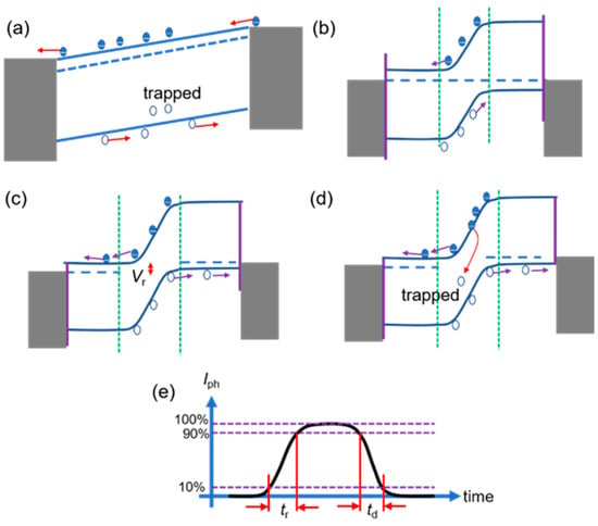
Figure 1. Schematic for gain and response time. (a) Photogenerated carrier transport in a photoconductor. (b–d) Photogenerated carrier transport in a photodiode. (b) Zero bias. (c) Reverse bias. (d) Reverse bias with hole traps in the depletion region. (e) Response time diagram. Rise time: tr. Decay time: td.
To induce gain in photodiodes, alternative carrier multiplication mechanisms are required. One such mechanism is avalanche breakdown, which induces impact ionization, resulting in carrier multiplication and gain in the detector. This phenomenon is widely used in avalanche photodiodes [56]. The induction of avalanche breakdown requires a large reverse bias. Recently, it has been reported that photogenerated hot carriers with sufficient energy can also lead to carrier multiplication, resulting in an EQE greater than 100% [57]. It is important to note that the photo energy must significantly exceed the band gap energy to induce impact ionization. The emergence of 2D/Si heterojunction photodetectors brings about unique properties, including gain. The gain in graphene/Si heterojunctions is well-explained and will be discussed later. However, the gain mechanism remains unclear for semiconducting 2D material/Si heterojunctions. For instance, zero bias semiconducting 2D material/Si heterojunction photodetectors have exhibited remarkably high responsivity, far surpassing the value calculated by Equation (6) [58][59][60][61]. Additionally, reverse biased semiconducting 2D material/Si heterojunctions without avalanche breakdown have also shown gain [62][63][64][65][66]. Therefore, further investigation into the gain mechanism in these heterojunctions is necessary.
4. Noise Equivalent Power
The minimum detectable signal of a photodetector is determined by its noise level. To quantify the ability to detect weak optical signals, the noise equivalent power (NEP) is commonly used. NEP is the incident light power required to achieve a signal-to-noise ratio of one within a bandwidth of 1 Hz [52]:
where in is the square root noise current per unit bandwidth with a unit of . The unit of the NEP is .
5. Detectivity and Specific Detectivity
A photodetector with a low NEP is preferred in order to achieve optimal performance. In the field of device characterization, it is common to use a parameter that quantifies the performance of a device, where a larger value indicates better performance. However, it is not desirable to state that a smaller parameter value corresponds to better device performance. To address this, another parameter called detectivity (D) is defined as the reciprocal of NEP, as shown in Equation (8):
It is important to note that the detectivity value depends on the photosensitive area of the device. To facilitate performance comparisons between photodetectors with different photosensitive areas, a parameter called specific detectivity (D*) is introduced, as shown in Equation (9):
where A is the photosensitive area of the device. The unit of specific detectivity is cm·Hz1/2/W, which is also written as Jones. For devices where shot noise dominates the noise characteristics, the D* is expressed as:
where Id is the dark current of the device. In the case of diode-like devices operating at zero bias, D* is expressed as [67]:
where Isat is the absolute value of the reverse saturation current. The specific detectivity provides a normalized value that takes into account both photosensitive area and bandwidth, enabling effective performance comparisons between different devices.
6. Response Time
The response time is a critical parameter that characterizes the performance of photodetectors. Typically, this parameter is represented by the rise time and decay time of a photodetector. The rise time and decay time are defined as the time required for the photocurrent to rise from 10% to 90% of its static value and vice versa, respectively, as shown in Figure 1e. The response time of a photoconductor is influenced by the lifetime of the photogenerated carriers and their mobility. In the case of diode-like photodetectors, the response time is determined by the diffusion time of carriers out of the depletion region, the drift time within the depleted region and the capacitance of the junction [51].
7. Linear Dynamic Range
In practical applications, it is crucial for a photodetector to have a linear response when converting optical signals into electrical signals in order to avoid distortion. However, at high light power levels, the photocurrent tends to saturate. To evaluate the linear response capability, the concept of linear dynamic range (LDR) is introduced. LDR represents the power range within which a photodetector maintains a linear response to incident light. It is defined as follows [68]:
Here, Pmin and Pmax correspond to the minimum and maximum light power levels, respectively, at which the photodetector exhibits linear response. The unit of LDR is decibel (dB). It is worth noting that most commercial photodiodes demonstrate linear response until they reach saturation. In these cases, Pmin represents the NEP without normalization to bandwidth. However, it is important to note that many photoconductive detectors reported in the literature exhibit sublinear behavior, making LDR inappropriate for characterizing them.
It is important to emphasize that the commonly misused definition of 20 lg(Pmax/Pmin) in the literature is incorrect. In engineering, the use of 10lg is appropriate for the power range with dB units, while 20lg is used for the amplitude range with dB units. Moreover, it is not appropriate to use photocurrent to define LDR as 20 lg(Ipmax/Ipmin), where Ipmax and Ipmin are the maximum and minimum photocurrents that the device responds linearly to incident light. This is because the focus should be on the linear response to incident light power and not on the photocurrent itself, making such a definition meaningless.
References
- Novoselov, K.S.; Geim, A.K.; Morozov, S.V.; Jiang, D.; Zhang, Y.; Dubonos, S.V.; Grigorieva, I.V.; Firsov, A.A. Electric field effect in atomically thin carbon films. Science 2004, 306, 666–669.
- Novoselov, K.S.; Jiang, D.; Schedin, F.; Booth, T.J.; Khotkevich, V.V.; Morozov, S.V.; Geim, A.K. Two-dimensional atomic crystals. Proc. Natl. Acad. Sci. USA 2005, 102, 10451–10453.
- Zhang, Y.B.; Tan, Y.W.; Stormer, H.L.; Kim, P. Experimental observation of the quantum Hall effect and Berry’s phase in graphene. Nature 2005, 438, 201–204.
- Castro, E.V.; Novoselov, K.S.; Morozov, S.V.; Peres, N.M.R.; Santos, J.D.; Nilsson, J.; Guinea, F.; Geim, A.K.; Neto, A.H.C. Biased bilayer graphene: Semiconductor with a gap tunable by the electric field effect. Phys. Rev. Lett. 2007, 99, 216802.
- Geim, A.K.; Novoselov, K.S. The rise of graphene. Nat. Mater. 2007, 6, 183–191.
- Liu, Y.; Duan, X.D.; Shin, H.J.; Park, S.; Huang, Y.; Duan, X.F. Promises and prospects of two-dimensional transistors. Nature 2021, 591, 43–53.
- Liu, C.S.; Chen, H.W.; Wang, S.Y.; Liu, Q.; Jiang, Y.G.; Zhang, D.W.; Liu, M.; Zhou, P. Two-dimensional materials for next-generation computing technologies. Nat. Nanotechnol. 2020, 15, 545–557.
- Akinwande, D.; Huyghebaert, C.; Wang, C.H.; Serna, M.I.; Goossens, S.; Li, L.J.; Wong, H.S.P.; Koppens, F.H.L. Graphene and two-dimensional materials for silicon technology. Nature 2019, 573, 507–518.
- Liu, Y.; Huang, Y.; Duan, X.F. Van der Waals integration before and beyond two-dimensional materials. Nature 2019, 567, 323–333.
- Splendiani, A.; Sun, L.; Zhang, Y.B.; Li, T.S.; Kim, J.; Chim, C.Y.; Galli, G.; Wang, F. Emerging Photoluminescence in Monolayer MoS2. Nano Lett. 2010, 10, 1271–1275.
- Mak, K.F.; Lee, C.; Hone, J.; Shan, J.; Heinz, T.F. Atomically Thin MoS2: A New Direct-Gap Semiconductor. Phys. Rev. Lett. 2010, 105, 136805.
- Bernardi, M.; Palummo, M.; Grossman, J.C. Extraordinary Sunlight Absorption and One Nanometer Thick Photovoltaics Using Two-Dimensional Monolayer Materials. Nano Lett. 2013, 13, 3664–3670.
- Britnell, L.; Ribeiro, R.M.; Eckmann, A.; Jalil, R.; Belle, B.D.; Mishchenko, A.; Kim, Y.J.; Gorbachev, R.V.; Georgiou, T.; Morozov, S.V.; et al. Strong Light-Matter Interactions in Heterostructures of Atomically Thin Films. Science 2013, 340, 1311–1314.
- Zeng, H.L.; Dai, J.F.; Yao, W.; Xiao, D.; Cui, X.D. Valley polarization in MoS2 monolayers by optical pumping. Nat. Nanotechnol. 2012, 7, 490–493.
- Mak, K.F.; He, K.L.; Shan, J.; Heinz, T.F. Control of valley polarization in monolayer MoS2 by optical helicity. Nat. Nanotechnol. 2012, 7, 494–498.
- Rivera, P.; Yu, H.Y.; Seyler, K.L.; Wilson, N.P.; Yao, W.; Xu, X.D. Interlayer valley excitons in heterobilayers of transition metal dichalcogenides. Nat. Nanotechnol. 2018, 13, 1004–1015.
- Kaul, A.B. Two-dimensional layered materials: Structure, properties, and prospects for device applications. J. Mater. Res. 2014, 29, 348–361.
- Neto, A.H.C.; Guinea, F.; Peres, N.M.R.; Novoselov, K.S.; Geim, A.K. The electronic properties of graphene. Rev. Mod. Phys. 2009, 81, 109–162.
- Zhou, J.D.; Lin, J.H.; Huang, X.W.; Zhou, Y.; Chen, Y.; Xia, J.; Wang, H.; Xie, Y.; Yu, H.M.; Lei, J.C.; et al. A library of atomically thin metal chalcogenides. Nature 2018, 556, 355–359.
- Kang, X.L.; Lan, C.Y.; Li, F.Z.; Wang, W.; Yip, S.; Meng, Y.; Wang, F.; Lai, Z.X.; Liu, C.T.; Ho, J.C. Van der Waals PdSe2/WS2 Heterostructures for Robust High-Performance Broadband Photodetection from Visible to Infrared Optical Communication Band. Adv. Opt. Mater. 2021, 9, 2001991.
- Jariwala, D.; Marks, T.J.; Hersam, M.C. Mixed-dimensional van der Waals heterostructures. Nat. Mater. 2017, 16, 170–181.
- Lan, C.Y.; Li, D.P.; Zhou, Z.Y.; Yip, S.P.; Zhang, H.; Shu, L.; Wei, R.J.; Dong, R.T.; Ho, J.C. Direct Visualization of Grain Boundaries in 2D Monolayer WS2 via Induced Growth of CdS Nanoparticle Chains. Small Methods 2019, 3, 1800245.
- Lan, C.Y.; Li, C.; Wang, S.; He, T.Y.; Zhou, Z.F.; Wei, D.P.; Guo, H.Y.; Yang, H.; Liu, Y. Highly responsive and broadband photodetectors based on WS2-graphene van der Waals epitaxial heterostructures. J. Mater. Chem. C 2017, 5, 1494–1500.
- Lan, C.Y.; Li, C.; Wang, S.; Yin, Y.; Guo, H.Y.; Liu, N.S.; Liu, Y. ZnO-WS2 heterostructures for enhanced ultra-violet photodetectors. RSC Adv. 2016, 6, 67520–67524.
- Jia, X.Y.; Lan, C.Y.; Li, C. Recent advances in two-dimensional materials in infrared photodetectors (invited). Infrared Laser Eng. 2022, 51, 20220065.
- Wu, D.; Xu, M.M.; Zeng, L.H.; Shi, Z.F.; Tian, Y.Z.; Li, X.J.; Shan, C.X.; Jie, J.S. In Situ Fabrication of PdSe2/GaN Schottky Junction for Polarization-Sensitive Ultraviolet Photodetection with High Dichroic Ratio. ACS Nano 2022, 16, 5545–5555.
- Wu, D.; Guo, J.W.; Wang, C.Q.; Ren, X.Y.; Chen, Y.S.; Lin, P.; Zeng, L.H.; Shi, Z.F.; Li, X.J.; Shan, C.X.; et al. Ultrabroadband and High-Detectivity Photodetector Based on WS2/Ge Heterojunction through Defect Engineering and Interface Passivation. ACS Nano 2021, 15, 10119–10129.
- Zeng, L.H.; Chen, Q.M.; Zhang, Z.X.; Wu, D.; Yuan, H.Y.; Li, Y.Y.; Qarony, W.; Lau, S.P.; Luo, L.B.; Tsang, Y.H. Multilayered PdSe2/Perovskite Schottky Junction for Fast, Self-Powered, Polarization-Sensitive, Broadband Photodetectors, and Image Sensor Application. Adv. Sci. 2019, 6, 1901134.
- Zeng, L.; Han, W.; Ren, X.; Li, X.; Wu, D.; Liu, S.; Wang, H.; Lau, S.P.; Tsang, Y.H.; Shan, C.-X.; et al. Uncooled Mid-Infrared Sensing Enabled by Chip-Integrated Low-Temperature-Grown 2D PdTe2 Dirac Semimetal. Nano Lett. 2023, 23, 8241–8248.
- Liang, S.J.; Cheng, B.; Cui, X.Y.; Miao, F. Van der Waals Heterostructures for High-Performance Device Applications: Challenges and Opportunities. Adv. Mater. 2020, 32, 1903800.
- Tang, Q.Y.; Zhong, F.; Li, Q.; Weng, J.L.; Li, J.Z.; Lu, H.Y.; Wu, H.T.; Liu, S.N.; Wang, J.C.; Deng, K.; et al. Infrared Photodetection from 2D/3D van der Waals Heterostructures. Nanomaterials 2023, 13, 1169.
- Behura, S.K.; Wang, C.; Wen, Y.; Berry, V. Graphene-semiconductor heterojunction sheds light on emerging photovoltaics. Nat. Photonics 2019, 13, 312–318.
- Yu, Y.; Wang, W.; Li, X.; Li, L.; Li, S.; Wei, X.; Zhou, W.; Lin, J.; Huang, Y.; Liu, H. Diameter-dependent photoelectric performances of semiconducting carbon nanotubes/perovskite heterojunctions. Nano Res. 2023, in press.
- Li, G.; Wang, Y.; Huang, L.; Sun, W. Research Progress of High-Sensitivity Perovskite Photodetectors: A Review of Photodetectors: Noise, Structure, and Materials. ACS Appl. Electron. Mater. 2022, 4, 1485–1505.
- Zhang, Z.; Ji, P.R.; Li, S.B.; Wang, F.; He, S.M.; Cheng, Y.W.; Zhao, S.H.; Li, K.L.; Wang, X.M.; Wang, Y.; et al. High-performance broadband flexible photodetector based on Gd3Fe5O12-assisted double van der Waals heterojunctions. Microsyst. Nanoeng. 2023, 9, 84.
- Sun, J.; Ding, L. Linearly Polarization-Sensitive Perovskite Photodetectors. Nano-Micro Lett. 2023, 15, 90.
- Wu, D.; Guo, J.W.; Du, J.; Xia, C.X.; Zeng, L.H.; Tian, Y.Z.; Shi, Z.F.; Tian, Y.T.; Li, X.J.; Tsang, Y.H.; et al. Polarization-Sensitive, Broadband, Self-Powered Photodetector Based on Graphene/PdSe2/Germanium Heterojunction. ACS Nano 2019, 13, 9907–9917.
- Zeng, L.H.; Lin, S.H.; Li, Z.J.; Zhang, Z.X.; Zhang, T.F.; Xie, C.; Mak, C.H.; Chai, Y.; Lau, S.P.; Luo, L.B.; et al. Fast, Self-Driven, Air-Stable, and Broadband Photodetector Based on Vertically Aligned PtSe2/GaAs Heterojunction. Adv. Funct. Mater. 2018, 28, 1705970.
- Yang, X.L.; Lin, J.; Huang, S.Y.; Lin, X.Y.; Xie, Y.Y.; Yan, F.P.; Zheng, W.; Kong, X.Z.; Hu, Q.C. Semiconductor applications of Yb2O3: Constructing heterojunction solar-blind UV photodetectors with graphene. Appl. Phys. Lett. 2023, 123, 081103.
- Wu, D.; Zhang, Y.; Liu, C.; Sun, Z.; Wang, Z.; Lin, Z.; Qiu, M.; Fu, D.; Wang, K. Recent Progress of Narrowband Perovskite Photodetectors: Fundamental Physics and Strategies. Adv. Devices Instrum. 2023, 4, 0006.
- Zeng, L.H.; Han, W.; Wu, S.E.; Wu, D.; Lau, S.P.; Tsang, Y.H. Graphene/PtSe2/Pyramid Si Van Der Waals Schottky Junction for Room-Temperature Broadband Infrared Light Detection. IEEE Trans. Electron Devices 2022, 69, 6212–6216.
- Huang, G.Y.; Hao, Y.B.; Li, S.Q.; Jia, Y.D.; Guo, J.C.; Zhang, H.; Wang, B. Recent progress in waveguide-integrated photodetectors based on 2D materials for infrared detection. J. Phys. D Appl. Phys. 2023, 56, 113001.
- Zeng, G.; Zhang, M.R.; Chen, Y.C.; Li, X.X.; Chen, D.B.; Shi, C.Y.; Zhao, X.F.; Chen, N.; Wang, T.Y.; Zhang, D.W.; et al. A solar-blind photodetector with ultrahigh rectification ratio and photoresponsivity based on the MoTe2/Ta:β-Ga2O3 pn junction. Mater. Today Phys. 2023, 33, 101042.
- Chang, C.; Xie, X.P.; Li, T.T.; Cui, J.S. Configuration of the active region for the Ge-on-Si photodetector based on carrier mobility. Front. Phys. 2023, 11, 1150684.
- Guo, Y.N.; Liu, D.; Miao, C.C.; Sun, J.M.; Pang, Z.Y.; Wang, P.; Xu, M.S.; Han, N.; Yang, Z.X. Ambipolar transport in Ni-catalyzed InGaAs nanowire field-effect transistors for near-infrared photodetection. Nanotechnology 2021, 32, 145203.
- Barve, A.V.; Lee, S.J.; Noh, S.K.; Krishna, S. Review of current progress in quantum dot infrared photodetectors. Laser Photonics Rev. 2010, 4, 738–750.
- An, X.H.; Liu, F.Z.; Jung, Y.J.; Kar, S. Tunable Graphene-Silicon Heterojunctions for Ultrasensitive Photodetection. Nano Lett. 2013, 13, 909–916.
- Peng, L.; Liu, L.X.; Du, S.C.; Bodepudi, S.C.; Li, L.F.; Liu, W.; Lai, R.C.; Cao, X.X.; Fang, W.Z.; Liu, Y.J.; et al. Macroscopic assembled graphene nanofilms based room temperature ultrafast mid-infrared photodetectors. InfoMat 2022, 4, e12309.
- Wu, D.; Guo, C.G.; Zeng, L.H.; Ren, X.Y.; Shi, Z.F.; Wen, L.; Chen, Q.; Zhang, M.; Li, X.J.; Shan, C.X.; et al. Phase-controlled van der Waals growth of wafer-scale 2D MoTe2 layers for integrated high-sensitivity broadband infrared photodetection. Light-Sci. Appl. 2023, 12, 5.
- Cai, X.; Wang, S.; Peng, L.-M. Recent progress of photodetector based on carbon nanotube film and application in optoelectronic integration. Nano Res. Energy 2023, 2, e9120058.
- Saleh, B.E.A.; Teich, M.C. Fundamentals of Photonics; John Wiley & Sons: Hoboken, NJ, USA, 2019; pp. 876–888.
- Kasap, S.O. Optoelectronics and Photonics: Principles and Practices, 2nd ed.; Pearson Education: Upper Saddle River, NJ, USA, 2013; pp. 381–427.
- Bube, R.H. Photoelectronic Properties of Semiconductors; Cambridge University Press: Cambridge, UK, 1992; pp. 20–21.
- Yang, M.; Chang, H.L.; Chen, J.H.; Zhu, X.Y. Multiplier Effects of Photodetectors-Source of Gain. Coatings 2023, 13, 1088.
- Song, Y.; Li, X.M.; Mackin, C.; Zhang, X.; Fang, W.J.; Palacios, T.; Zhu, H.W.; Kong, J. Role of Interfacial Oxide in High-Efficiency Graphene-Silicon Schottky Barrier Solar Cells. Nano Lett. 2015, 15, 2104–2110.
- Song, J.; Bin, S.; Zhou, C.; Qin, B. High-Performance Normal-Incidence Ge/Si Meta-Structure Avalanche Photodetector. Photonics 2023, 10, 780.
- Garin, M.; Heinonen, J.; Werner, L.; Pasanen, T.P.; Vahanissi, V.; Haarahiltunen, A.; Juntunen, M.A.; Savin, H. Black-Silicon Ultraviolet Photodiodes Achieve External Quantum Efficiency above 130%. Phys. Rev. Lett. 2020, 125, 117702.
- Xiao, P.; Mao, J.; Ding, K.; Luo, W.J.; Hu, W.D.; Zhang, X.J.; Zhang, X.H.; Jie, J.S. Solution-Processed 3D RGO-MoS2/Pyramid Si Heterojunction for Ultrahigh Detectivity and Ultra-Broadband Photodetection. Adv. Mater. 2018, 30, 1801729.
- Wu, D.; Lou, Z.H.; Wang, Y.G.; Yao, Z.Q.; Xu, T.T.; Shi, Z.F.; Xu, J.M.; Tian, Y.T.; Li, X.J.; Tsang, Y.H. Photovoltaic high-performance broadband photodetector based on MoS2/Si nanowire array heterojunction. Sol. Energy Mater. Sol. Cells 2018, 182, 272–280.
- Ye, P.; Xiao, H.; Zhu, Q.H.; Kong, Y.H.; Tang, Y.M.; Xu, M.S. Si-CMOS-compatible 2D PtSe2-based self-driven photodetector with ultrahigh responsivity and specific detectivity. Sci. China Mater. 2023, 66, 193–201.
- Li, L.; Xu, H.; Li, Z.; Liu, L.; Lou, Z.; Wang, L. CMOS-Compatible Tellurium/Silicon Ultra-Fast Near-Infrared Photodetector. Small 2023, 2303114.
- Li, Y.; Xu, C.Y.; Wang, J.Y.; Zhen, L. Photodiode-Like Behavior and Excellent Photoresponse of Vertical Si/Monolayer MoS2 Heterostructures. Sci. Rep. 2014, 4, 7186.
- Shin, G.H.; Park, J.; Lee, K.J.; Lee, G.B.; Jeon, H.B.; Choi, Y.K.; Yu, K.; Choi, S.Y. Si-MoS2 Vertical Heterojunction for a Photodetector with High Responsivity and Low Noise Equivalent Power. ACS Appl. Mater. Interfaces 2019, 11, 7626–7634.
- Wang, Z.Y.; Zhang, X.W.; Wu, D.; Guo, J.W.; Zhao, Z.H.; Shi, Z.F.; Tian, Y.T.; Huang, X.W.; Li, X.J. Construction of mixed-dimensional WS2/Si heterojunctions for high-performance infrared photodetection and imaging applications. J. Mater. Chem. C 2020, 8, 6877–6882.
- Pal, S.; Mukherjee, S.; Jangir, R.; Nand, M.; Jana, D.; Mandal, S.K.; Bhunia, S.; Mukherjee, C.; Jha, S.N.; Ray, S.K. WS2 Nanosheet/Si p-n Heterojunction Diodes for UV-Visible Broadband Photodetection. ACS Appl. Nano Mater. 2021, 4, 3241–3251.
- Lu, J.T.; Zhang, L.J.; Ma, C.R.; Huang, W.J.; Ye, Q.J.; Yi, H.X.; Zheng, Z.Q.; Yang, G.W.; Liu, C.A.; Yao, J.D. In situ integration of Te/Si 2D/3D heterojunction photodetectors toward UV-vis-IR ultra-broadband photoelectric technologies. Nanoscale 2022, 14, 6228–6238.
- Rogalski, A. Infrared and Terahertz Detectors, 3rd ed.; CRC Press: New York, NY, USA, 2019; p. 252.
- Liu, J.-M. Principles of Photonics; Cambridge University Press: Cambridge, UK, 2016; p. 388.
More
Information
Subjects:
Physics, Applied
Contributors
MDPI registered users' name will be linked to their SciProfiles pages. To register with us, please refer to https://encyclopedia.pub/register
:
View Times:
2.3K
Revisions:
2 times
(View History)
Update Date:
09 Oct 2023
Table of Contents


Notice
You are not a member of the advisory board for this topic. If you want to update advisory board member profile, please contact office@encyclopedia.pub.
OK
Confirm
Only members of the Encyclopedia advisory board for this topic are allowed to note entries. Would you like to become an advisory board member of the Encyclopedia?
Yes
No
${ textCharacter }/${ maxCharacter }
Submit
Cancel
Back
Comments
${ item }
|
${ item.createdUser.fullName }
${ item.createdAt }
${ item.vote }
${ item.reply }
Delete
${ reply.createdUser.fullName }
${ reply.createdAt }
${ reply.vote }
Delete
There is no reply to this comment~
${ item.replyTextCharacter }/${ item.replyMaxCharacter }
Submit
Cancel
More
No more~
There is no comment~
${ textCharacter }/${ maxCharacter }
Submit
Cancel
${ selectedItem.replyTextCharacter }/${ selectedItem.replyMaxCharacter }
Submit
Cancel
Confirm
Are you sure to Delete?
Yes
No