Your browser does not fully support modern features. Please upgrade for a smoother experience.
Submitted Successfully!
 +1 credit
Thank you for your contribution! You can also upload a video entry or images related to this topic.
For video creation, please contact our Academic Video Service.
| Version | Summary | Created by | Modification | Content Size | Created at | Operation |
|---|---|---|---|---|---|---|
| 1 | Raul Gregor | -- | 2254 | 2023-09-21 15:39:26 | | | |
| 2 | Lindsay Dong | Meta information modification | 2254 | 2023-09-22 16:16:32 | | | | |
| 3 | Lindsay Dong | + 6 word(s) | 2260 | 2023-09-22 16:19:40 | | |
Video Upload Options
We provide professional Academic Video Service to translate complex research into visually appealing presentations. Would you like to try it?
Cite
If you have any further questions, please contact Encyclopedia Editorial Office.
Gregor, R.; Toledo, S.; Maqueda, E.; Pacher, J. Advancements in Power Converter Technologies. Encyclopedia. Available online: https://encyclopedia.pub/entry/49486 (accessed on 26 July 2026).
Gregor R, Toledo S, Maqueda E, Pacher J. Advancements in Power Converter Technologies. Encyclopedia. Available at: https://encyclopedia.pub/entry/49486. Accessed July 26, 2026.
Gregor, Raúl, Sergio Toledo, Edgar Maqueda, Julio Pacher. "Advancements in Power Converter Technologies" Encyclopedia, https://encyclopedia.pub/entry/49486 (accessed July 26, 2026).
Gregor, R., Toledo, S., Maqueda, E., & Pacher, J. (2023, September 21). Advancements in Power Converter Technologies. In Encyclopedia. https://encyclopedia.pub/entry/49486
Gregor, Raúl, et al. "Advancements in Power Converter Technologies." Encyclopedia. Web. 21 September, 2023.
Copy Citation
Power converter technologies have become vital in various applications due to their efficient management of electrical energy. With the growing prominence of renewable energy sources such as solar and wind, the high penetration of power electronic converters has been justified. However, ensuring power quality has emerged as a significant challenge for grid-connected power converters.
power converters
SiC-MOSFET
voltage source converters
power quality
modular multilevel converter
cascade H-Bridge
1. Introduction
Nowadays, power converter technologies play a significant role in various applications, such as electric transportation [1], electric aircraft [2][3], and energy conversion systems [4][5], due to their efficient management of electrical energy. The increasing adoption of power electronic converters in energy systems can be attributed to the growing use of renewable energies such as solar and wind power [6]. In renewable energy applications, addressing power quality has become a primary concern for all grid-connected power converters to comply with grid codes [7][8]. In this sense, power quality issues involve deviations from the ideal sinusoidal waveform in magnitude and frequency, impacting both grid- and load-side currents and voltages [9][10]. Recent research has proposed various approaches to enhance the efficiency of voltage source converters (VSC) and mitigate power-quality-related losses [11][12][13]. The rapid progress in power converters has been furthered by the development of high-performance microprocessors capable of implementing advanced nonlinear digital controllers. Moreover, the field of power electronic semiconductors has made significant strides in creating new high-speed switching devices with remarkably low on-state losses.
From the point of view of the conventional AC-DC-AC, the two-level voltage source converters (2L-VSCs) are still some of the most used converters for many applications, and, nowadays, the 2L-VSCs are considered the fundamental components in both industrial applications and renewable energies. However, the limited number of output voltage levels creates challenges related to losses and power quality, attributed to their unfavorable harmonic profiles [14][15]. In this sense, the modular multilevel converter (MMC) has garnered attention from the industry and energy sectors, due to its ability to solve the problems associated with harmonic distortion. This converter demonstrates the ability to generate sinusoidal voltages and currents with minimal harmonic distortions. Among the MMC topologies, the cascade H-Bridge (CHB) configuration stands out as a popular choice due to its inherent modularity, facilitating scalability to generate higher MMC voltage levels. Additionally, the CHB-based MMC design avoids the need to incorporate an extensive array of flying capacitors or clamping diodes in the power converter topology [16]. Consequently, one of the most widely discussed topologies in the literature is the seven-level voltage source converter (7L-VSC) based on three CHB cells in series per phase [17]. However, both 2L-VSC and 7L-VSC topologies are based on AC-DC-AC configurations, which require the inclusion of an intermediate stage of energy storage elements such as capacitor banks. These additional components contribute to increased weight and volume, and, above all, these capacitors add the possibility of failure in the VSCs.
Among these VSC topologies, the most commonly employed power semiconductor devices are IGBTs. However, SiC-MOSFETs have gained attention as an alternative due to their ability to operate at higher switching frequencies compared to IGBTs [18][19][20]. Nevertheless, simply incorporating faster switching devices is insufficient to improve power quality. It is crucial to prioritize the design of the entire converter to ensure enhanced performance at high switching frequencies with power semiconductor devices [21][22].
2. H-Bridge Cell-Based Converters
In recent years, the trend in power electronics design has shifted towards modular solutions. Modularity enables the scalability of the converter, allowing for an increase in power capacity by arranging several H-Bridge cells in parallel. Alternatively, assembling cells in series can result in a multilevel converter. A modular design for an H-Bridge cell must consider various aspects, such as the switching signals of the power semiconductors, the generation of dead times, and the implementation of protection circuits. These considerations are essential to provide robustness to the H-Bridge cell and ensure its reliable operation. Furthermore, the use of a modular approach can also simplify maintenance and repair processes, as individual cells can be replaced if necessary, without affecting the entire system. Overall, the modular design approach offers several advantages, including scalability, robustness, and ease of maintenance, making it a popular choice for power converter design [23]. The subsequent sections cover the electronic circuits of each module comprising an H-Bridge cell.
2.1. Switching Signal Drivers
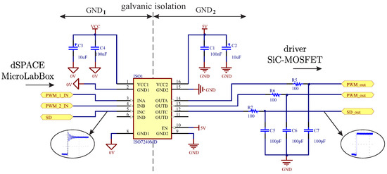
The switching signal drivers are essential components in the control circuits of SiC-MOSFET semiconductor devices; they ensure the proper operation of the power conversion system. However, these drivers are susceptible to the electrical noise generated by the high-frequency switching of the power semiconductor device. To overcome this issue, it is necessary to incorporate a galvanic isolation stage in the driver circuit. This galvanic isolation stage helps in achieving immunity to electrical noise and ensures the stable operation of the power conversion system. The driver circuit, as shown in Figure 1, exhibits an under-damped characteristic of the input signal from the control module to the galvanic isolator. To compensate for this under-damping, a passive low-pass filter is used. The design of this filter takes into consideration the maximum switching frequency of the power semiconductor device, and it helps in reducing the noise and improving the performance of the driver circuit.
Figure 1. Switching signal conditioning circuit.
2.2. Dead Time Generation Circuit
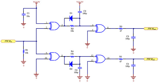
In addition to galvanic isolation, it is also crucial to implement dead time in the complementary signals applied to the half-H-Bridge. Dead time is a brief interval where both switches in the half-H-Bridge are turned off to avoid short circuits between edge changes in the switching signals [24]. This ensures that the output voltage is always proportional to the control signal and reduces the likelihood of power device failure due to short circuits. Figure 2 displays the driver circuitry, where the application of dead time is evident in the complementary signals [25]. The input signal from the control module to the galvanic isolator exhibits an under-damped characteristic, which is compensated for by the use of a passive low-pass filter. The filter is designed to suppress high-frequency noise generated by the switching of the power semiconductor device, while considering the maximum switching frequency.
Figure 2. Dead time generation circuit.
2.3. Gate Complementary Signal Generation
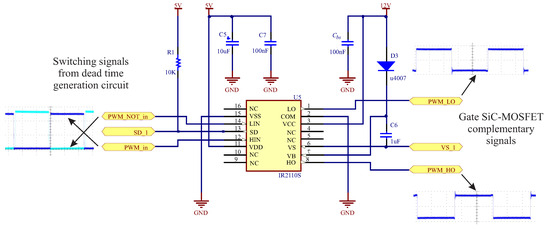
The IR2110S device, as a high-voltage, high-speed power MOSFET and IGBT driver with independent high- and low-side referenced output channels, is crucial in properly driving the high-side devices of a bridge circuit, as well as the low-side devices. As shown in Figure 3, the gate driver circuit employs a bootstrap circuit, which provides the required voltage to the high-side devices. Specifically, the bootstrap capacitor C1 is charged by the voltage across the low-side device and then used to switch the high-side device [26]. The advantage of this configuration is that it allows for the use of a single isolated power supply for the driver circuit, thereby reducing the overall system complexity and cost. Moreover, the IR2110S device incorporates an under-voltage lockout function, which ensures that the power MOSFETs and IGBTs are not damaged due to insufficient voltage levels, thus improving the reliability of the circuit.
Figure 3. Gate SiC-MOSFET complementary signal generation.
2.4. Power Board for the H-Bridge
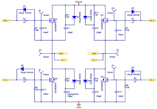
The multilevel converter design approach seeks to combine cells in an H-Bridge arrangement, connecting them in series to achieve higher output voltage levels. This configuration allows us to achieve a scalable and modular design. The device selected to mount the power board for the H-Bridge cell design is CREE Semiconductor’s CAS120M12BM2, which is a power component that features two SiC-MOSFET transistors connected in a half-H-Bridge configuration. This device is characterized by low conduction resistance and a significantly higher switching speed than conventional switching devices such as IGBTs. Figure 4 shows the scheme proposed for the design of the power board for the complete H-Bridge scheme.
Figure 4. Electrical schematic of the H-Bridge based on SiC-MOSFET semiconductor device.
3. Two-Level Multimodular VSC Topology
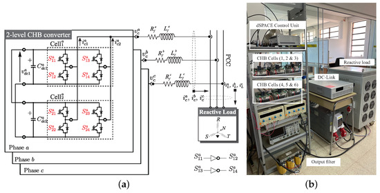
The scalable 2L-VSC topology consists of parallel-connected H-Bridge cells, as shown in the schematic of Figure 5a. The modular characteristic makes it particularly useful for applications where a compact converter, high energy density, and good reliability are required. This is possible by incorporating a redundant scheme, constituting an advantage compared to conventional converters. The characteristics of a simple and compact power circuit, scalability in terms of nominal power, and the possibility of operation in the event of faults due to the redundancy of modules connected in parallel result in a more robust, economical, and flexible VSC compared to traditional configurations.
Figure 5. Two-level multimodular VSC. (a) Modular two-level CHB-based VSC. (b) Two-level CHB-based VSC experimental test bench.
From the point of view of the power semiconductor devices, SiC-MOSFETs have a comparative advantage in terms of switching losses and switching frequencies, compared to IGBT-type semiconductor devices. The implemented scalable multimodular 2L-VSC, which is shown in Figure 5b, integrates SiC-MOSFET-type semiconductors, and its switching hardware has been designed to achieve switching frequencies close to 100 kHz.
4. Seven-Level Multimodular VSC Topology
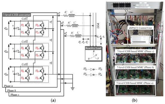
The scalable 7L-VSC topology, which is based on CHB cells, consists of three independent cells per phase connected in series with an independent DC-link ( ), as depicted in Figure 6a. This operational scheme incorporates SiC-MOSFET switching semiconductor devices and an output inductance 𝐿𝑓, which operates as a filter at the output of the converter. The DC-link voltage ( ) serves as the energy source, while the switching semiconductors synthesize the signals that are injected into the load at the connection point. The output inductance attenuates the harmonic effects resulting from the switching of the power devices in the converter. Figure 6b illustrates the integration of the different elements that comprise the experimental test bench of the 7L-VSC. One notable advantage of this design is its versatility and modularity, allowing for multiple configurations with minimal changes to the converter’s structure. Additionally, it is possible to expand the number of levels by adding more cascaded cells.
Figure 6. Seven-level multimodular VSC. (a) Modular 7-level CHB-based VSC. (b) The 7-level CHB-based VSC experimental test bench.
5. Voltage Source Matrix Converter Topology
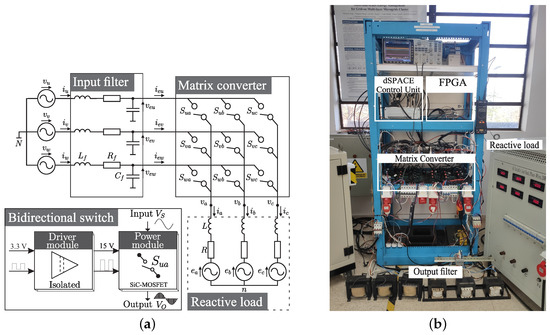
The matrix converter (MC) is a single-stage AC-AC converter capable of directly supplying an “n” phase load from an “m” phase source (𝑚×𝑛 MC), without the need for intermediate AC-DC conversion stages [27]. The main advantages of MCs compared to widely used back-to-back conversion systems, which consist of rectifier stages connected to an inverter with an intermediate energy storage stage (capacitor bank), are as follows: reduced size, light weight and long lifespan due to the absence of large electrolytic capacitors in the main circuit, and high efficiency due to the single power conversion stage, resulting in fewer switch losses compared to two-stage converters. Given these advantages, MCs are currently used in a wide range of AC-AC conversion applications, such as industrial applications requiring variable-speed electric motor drives, electric mobility, and, more recently, wind energy conversion systems [28][29]. The general topology for the MC is shown in Figure 7a. In this case, a voltage source matrix converter (VSMC) is obtained. To achieve good performance, the VSMC should be equipped with a source filter. The source filter is generally required to minimize high-frequency components in the input currents and reduce the impact of disturbances on the input grid. However, the size of the filter elements is inversely proportional to the VSMC’s switching frequency. Figure 7b shows the implemented experimental setup of the VSMC based on bidirectional switches designed using SiC-MOSFET semiconductor devices.
Figure 7. Matrix converter. (a) Voltage source matrix converter topology. (b) Voltage source matrix converter experimental test bench.
5.1. Bidirectional Switch Design
The bidirectional switch (Bi-Sw) design is divided into two main parts, the dominated control block and power block, respectively. Figure 10a shows the block diagram of the basic Bi-Sw operation. The control module performs signal conditioning for the voltage and current levels (3.3 V to 15 V) required by the power module for the proper operation of its components and electrical noise isolation. The power module is based on the SiC-MOSFET semiconductor device, which essentially works in cut-off and saturation zones at all times, controlling the current flow in both directions. The driver module has been implemented using the ISO5500 device. The ISO5500 is a gate driver device for IGBT and power MOSFET semiconductors; it has TTL input and a power output separated by a capacitive isolation barrier. This isolation barrier means that there is separation between the input signal grounds and the power stage, preventing voltage and current noise produced by high switching and power, which can disturb digital control devices.
5.2. Voltage Source Matrix Converter Experimental Results
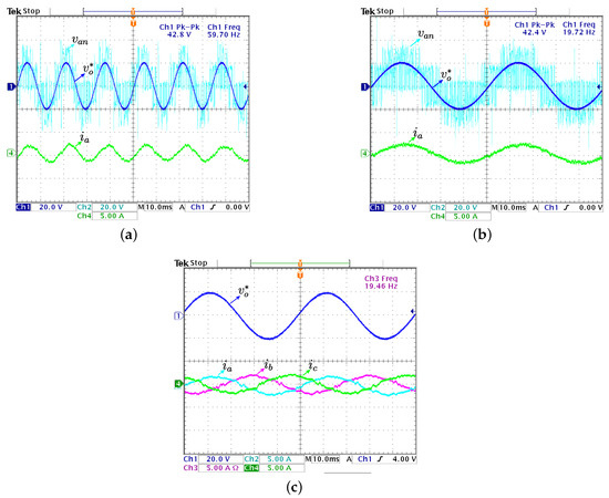
VSMC testing is performed using the experimental test bench described in Figure 7b, where an AC voltage variator is used as an input source and the output balances a three-phase load type 𝑅𝐿 connected in star with values equal to R = 16Ω and L = 10 mH. For this test, the space vector modulation (SVM) strategy is used, in which the 27 valid vectors of the MC are used to obtain a desired output voltage. For the implementation of the SVM, it is necessary to measure the input voltages (𝑣𝑒𝑢,𝑣𝑒𝑣,𝑣𝑒𝑤) to the VSMC. The results in Figure 8 are obtained at a sampling frequency 𝑓𝑠=50 kHz. In Figure 8a, the waveforms of the output voltage 𝑣𝑎𝑛 and output current 𝑖𝑎 are observed for a reference 𝑣𝑜∗ = 20 V/60 Hz, and, in Figure 8b, the same test is performed but for a frequency of 𝑣𝑜∗ = 20 V/20 Hz. The waveforms of the three-phase output currents are shown in Figure 8c. The results obtained show correct tracking in the desired reference, and the output currents on the 𝑅𝐿 load present the expected sinusoidal shape.
Figure 8. Experimental results of output voltage and current using an SVM to MC with 𝑅𝐿 load (R = 16Ω and L = 10 mH). (a) Tracking for a 𝑣∗𝑜 = 20 V/60 Hz. (b) Tracking for a 𝑣∗𝑜 = 20 V/20 Hz. (c) MC output current for a 𝑣∗𝑜 = 20 V/20 Hz.
References
- Frikha, M.; Croonen, J.; Deepak, K.; Benômar, Y.; El Baghdadi, M.; Hegazy, O. Multiphase Motors and Drive Systems for Electric Vehicle Powertrains: State of the Art Analysis and Future Trends. Energies 2023, 16, 768.
- Russo, A.; Cavallo, A. Stability and Control for Buck–Boost Converter for Aeronautic Power Management. Energies 2023, 16, 988.
- Russo, A.; Cavallo, A. Supercapacitor stability and control for More Electric Aircraft application. In Proceedings of the 2020 European Control Conference (ECC), St. Petersburg, Russia, 12–15 May 2020; pp. 1909–1914.
- Athwer, A.; Darwish, A. A Review on Modular Converter Topologies Based on WBG Semiconductor Devices in Wind Energy Conversion Systems. Energies 2023, 16, 5324.
- Murillo-Yarce, D.; Rivera, M.; Restrepo, C.; Rodríguez, R.; Wheeler, P.W.; Zanchetta, P.; Mirzaeva, G. Sequential Predictive Current Control of a VSI with Common-Mode Voltage Reduction. In Proceedings of the 10th International Conference on Power Electronics, Machines and Drives (PEMD 2020), Online, 15–17 December 2020; pp. 651–656.
- Milev, K.; Yaramasu, V.; Dekka, A.; Kouro, S. Predictive control of multichannel boost converter and VSI-based six-phase PMSG wind energy systems with fixed switching frequency. In Proceedings of the IEEE Proceeding PEDSTC, Tehran, Iran, 4–6 February 2020; pp. 1–6.
- Abdelaziz, F.; Azzouz, Z.e.; Omari, A. Common mode voltage mitigation using a new modified model predictive control (mmpc) in a three phase voltage source inverter. In Proceedings of the ENERGYCon, Gammarth, Tunisia, 28 September–1 October 2020; pp. 93–97.
- Gil-González, W.; Escobar-Mejía, A.; Montoya-Giraldo, O. Model Predictive Direct Power Control Applied to Grid-Connected Voltage Source Inverters. In Proceedings of the PEDG, Dubrovnik, Croatia, 28 September–1 October 2020; pp. 610–614.
- Xu, J.; Soeiro, T.B.; Gao, F.; Chen, L.; Tang, H.; Bauer, P.; Dragičević, T. Carrier-based modulated model predictive control strategy for three-phase two-level VSIs. Trans. Energy Conver. 2021, 36, 1673–1687.
- Rojas, D.; Rivera, M.; Toledo, S.; Wheeler, P. Predictive control techniques applied to a 2L-VSI. In Proceedings of the CHILECON, Valparaíso, Chile, 6–9 December 2021; pp. 1–6.
- Rojas, D.; Rivera, M.; Muñoz, J.; Wheeler, P. Cascaded predictive control for a three-phase VSI with different cost functions. In Proceedings of the CHILECON, Valparaíso, Chile, 6–9 December 2021; pp. 1–6.
- Xu, J.; Gao, F.; Soeiro, T.B.; Chen, L.; Tarisciotti, L.; Tang, H.; Bauer, P. Model Predictive Control for the Reduction of DC-link Current Ripple in Two-level Three-phase Voltage Source Inverters. In Proceedings of the ECCE, Lyon, France, 7–11 September 2020; p. P-1.
- Pacher, J.; Rodas, J.; Renault, A.; Ayala, M.; Comparatore, L.; Gregor, R. Design and validation of a multilevel voltage source inverter based on modular H-bridge cells. HardwareX 2023, 15, e00452.
- Comparatore, L.; Renault, A.; Pacher, J.; Rodas, J.; Gregor, R. Finite Control Set Model Predictive Control Strategies for a Three-Phase Seven-level Cascade H-Bridge DSTATCOM. In Proceedings of the IEEE Proceeding ICRERA, Paris, France, 14–17 October 2018; pp. 779–784.
- Xu, Z.; Liu, Y.; Cao, B.; Liu, B.; Li, S. Research and Application of Compensation Characteristics of DSTATCOM under Unbalanced Load. In Proceedings of the IEEE Proceeding IAEAC, Chongqing, China, 12–14 October 2018; pp. 806–810.
- Renault, A.; Rodas, J.; Comparatore, L.; Pacher, J.; Gregor, R. Modulated Predictive Current Control Technique for a Three-Phase Four-Wire Active Power Filter based on H-bridge Two-Level Converter. In Proceedings of the IEEE Proceeding UPEC, Glasgow, UK, 4–7 September 2018; pp. 1–6.
- Kehl, Z.; Glasberger, T.; Peroutka, Z. Finite Control Set Model Predictive Control of Static Compensator. In Proceedings of the IEEE Proceeding ISIE, Vancouver, BC, Canada, 12–14 June 2019; pp. 858–863.
- Renault, A.; Ayala, M.; Comparatore, L.; Pacher, J.; Gregor, R. Comparative Study of Predictive-Fixed Switching Techniques for a Cascaded H-Bridge Two level STATCOM. In Proceedings of the IEEE Proceeding UPEC, Glasgow, UK, 4–7 September 2018; pp. 1–6.
- Maqueda, E.; Toledo, S.; Gregor, R.; Caballero, D.; Gavilán, F.; Rodas, J.; Rivera, M.; Wheeler, P. An assessment of predictive current control applied to the direct matrix converter based on SiC-MOSFET bidirectional switches. In Proceedings of the 2017 IEEE Southern Power Electronics Conference (SPEC), Puerto Varas, Chile, 4–7 December 2017; pp. 1–6.
- Pacher, J.; Rodas, J.; Gregor, R.; Rivera, M.; Renault, A.; Comparatore, L. Efficiency analysis of a modular H-bridge based on SiC MOSFET. Taylor Fr. Trans. 2019, 7, 59–67.
- Ipoum-Ngome, P.G.; Mon-Nzongo, D.L.; Flesch, R.C.C.; Song-Manguelle, J.; Wang, M.; Jin, T. Model-free predictive current control for multilevel voltage source inverters. Trans. Ind. Electron. 2020, 68, 9984–9997.
- Vu, H.C.; Lee, H.H. Model-Predictive Current Control Scheme for Seven-Phase Voltage-Source Inverter With Reduced Common-Mode Voltage and Current Harmonics. IEEE J. Emerg. Sel. Top. Power Electron. 2020, 9, 3610–3621.
- Zhang, L.; Yuan, X.; Wu, X.; Shi, C.; Zhang, J.; Zhang, Y. Performance evaluation of high-power SiC MOSFET modules in comparison to Si IGBT modules. IEEE Trans. Power Electron. 2019, 34, 1181–1196.
- Jiao, N.; Wang, S.; Liu, T.; Wang, Y.; Chen, Z. Harmonic Quantitative Analysis for Dead-Time Effects in SPWM Inverters. IEEE Access 2019, 7, 43143–43152.
- Li, B.; Xu, J.; Ye, J.; Wang, H.; Huang, S.; Li, Y.; Shen, A. A New Model-Based Dead-Time Compensation Strategy for Cascaded H-Bridge Converters. IEEE Trans. Ind. Electron. 2023, 70, 3793–3802.
- Infineon-Semiconductors. 600 V High and Low Side Driver IC. 2017. Available online: https://www.infineon.com/dgdl/Infineon-IR2110-DataSheet (accessed on 7 March 2023).
- Gili, L.C.; Dias, J.C.; Lazzarin, T.B. Review, Challenges and Potential of AC/AC Matrix Converters CMC, MMMC, and M3C. Energies 2022, 15, 9421.
- Toledo, S.; Caballero, D.; Maqueda, E.; Cáceres, J.J.; Rivera, M.; Gregor, R.; Wheeler, P. Predictive Control Applied to Matrix Converters: A Systematic Literature Review. Energies 2022, 15, 7801.
- Diaz, M.; Cárdenas Dobson, R.; Ibaceta, E.; Mora, A.; Urrutia, M.; Espinoza, M.; Rojas, F.; Wheeler, P. An Overview of Applications of the Modular Multilevel Matrix Converter. Energies 2020, 13, 5546.
More
Information
Subjects:
Engineering, Electrical & Electronic
Contributors
MDPI registered users' name will be linked to their SciProfiles pages. To register with us, please refer to https://encyclopedia.pub/register
:
View Times:
607
Revisions:
3 times
(View History)
Update Date:
22 Sep 2023
Table of Contents


Notice
You are not a member of the advisory board for this topic. If you want to update advisory board member profile, please contact office@encyclopedia.pub.
OK
Confirm
Only members of the Encyclopedia advisory board for this topic are allowed to note entries. Would you like to become an advisory board member of the Encyclopedia?
Yes
No
${ textCharacter }/${ maxCharacter }
Submit
Cancel
Back
Comments
${ item }
|
${ item.createdUser.fullName }
${ item.createdAt }
${ item.vote }
${ item.reply }
Delete
${ reply.createdUser.fullName }
${ reply.createdAt }
${ reply.vote }
Delete
There is no reply to this comment~
${ item.replyTextCharacter }/${ item.replyMaxCharacter }
Submit
Cancel
More
No more~
There is no comment~
${ textCharacter }/${ maxCharacter }
Submit
Cancel
${ selectedItem.replyTextCharacter }/${ selectedItem.replyMaxCharacter }
Submit
Cancel
Confirm
Are you sure to Delete?
Yes
No