 +1 credit
| Version | Summary | Created by | Modification | Content Size | Created at | Operation |
|---|---|---|---|---|---|---|
| 1 | Gyórgy Sáfrán | -- | 3723 | 2023-07-17 14:21:35 | | | |
| 2 | Gyórgy Sáfrán | + 4 word(s) | 3727 | 2023-07-17 14:24:37 | | | | |
| 3 | Gyórgy Sáfrán | Meta information modification | 3727 | 2023-07-17 14:29:26 | | | | |
| 4 | Rita Xu | -3 word(s) | 3724 | 2023-07-18 03:28:35 | | | | |
| 5 | Rita Xu | Meta information modification | 3724 | 2023-07-18 03:43:13 | | | | |
| 6 | Rita Xu | Meta information modification | 3724 | 2023-07-18 03:47:09 | | |
Video Upload Options
The novel, single-sample concept combinatorial method, the so-called micro-combinatory technique, has been shown to be suitable for the high-throughput and complex characterization of multicomponent thin films over an entire composition range. In addition to the 3 mm diameter TEM grid used for microstructural analysis, by scaling up the substrate size to 10 × 25 mm, this novel approach has allowed for a comprehensive study of the properties of the materials as a function of their composition, which has been determined via transmission electron microscopy (TEM), scanning electron microscopy (SEM), Rutherford backscattering spectrometry (RBS), X-ray diffraction analysis (XRD), atomic force microscopy (AFM), spectroscopic ellipsometry, and nanoindentation studies.
1. Introduction
Combinatorics, also known as combinatorial mathematics, concerns the problems of selection, arrangement, and operation within finite or discrete systems [1]. The combinatorial approach is ubiquitous, regardless of the involvement of mathematics. Indeed, the evolution of life on Earth is the greatest combinatorial experiment. Mother Nature conducts this experiment with millions of species and billions of individuals at a time through their confrontation with a changing environment, which, over millions of years, selects such individuals for survival and successful reproduction.
Even in our everyday lives, we use combinatorial approaches almost instinctively to organize and group our programs and tasks efficiently to save time, effort, and money.
Researchers can learn from nature and apply combinatorial solutions, preferably consciously instead of synthesizing and characterizing many individual samples. They can simultaneously use combinatorial techniques, collect or create groups of samples, and test them or have them interact with the environment to study their behavior more efficiently. Mother Nature’s infinite possibilities are a good fit with the trial-and-error approach, but due to humanity’s severely limited possibilities, researchers need to design their combinatorial experiments carefully.
One of the first combinatorial experiments for solving practical problems was published by Dorfman [2] during World War 2. He proposed a high-throughput method for screening syphilitic individuals from a large population of recruits. Since individual testing would have required great efforts and expenses and the incidence of the disease was only a few cases out of tens of thousands, he proposed group testing such that soldiers were divided into groups of one hundred individuals, whose blood samples were then pooled. The few pooled samples that presented the syphilis antigen were selected, and only persons from whom these samples originated were evaluated individually. This reduced the work and costs required by more than an order of magnitude. Dorfman’s example has clearly proven the benefits of combinatorial solutions.
In terms of materials science and technology, the structural, physical, and chemical properties of innovative materials depend largely on the proportion of their components. The traditional method for characterizing binaries and ternaries over a wide range of compositions is to synthesize and evaluate many samples, one for each composition, which is obviously inefficient. In contrast to individual studies, combinatorial techniques allow for the high-throughput characterization of compounds, thereby enabling the performance of comprehensive characterizations or even the creation of materials databases in a short time and with less effort.
2. Applications of the Micro-Combinatorial Technique in Materials Science
2.1. Al-Mn Thin Layer System
Upon heat treatment, bulk MnAl in the concentration range of 50–60 at%Mn undergoes a transformation from a hexagonal ε-MnAl phase to a metastable, ferromagnetic, tetragonal L10 τ-MnAl phase [3][4]. Due to the high coercivity of the τ-phase, MnAl may be a suitable substitute for the Pt used in FePt and CoPt hard magnetic coatings, e.g., in recording media. However, different additional phases may exist in thin films, and the concentration range of the different phases known in the bulk state may differ in composition. This calls for a comprehensive study of the structure and morphology of the MnAl thin film system, for which the efficient micro-combinatorial method is well suited [5][6]. A variable concentration Mn-Al sample has been deposited at room temperature onto a Mo TEM grid covered with a SiOx support layer (see Figure 1).
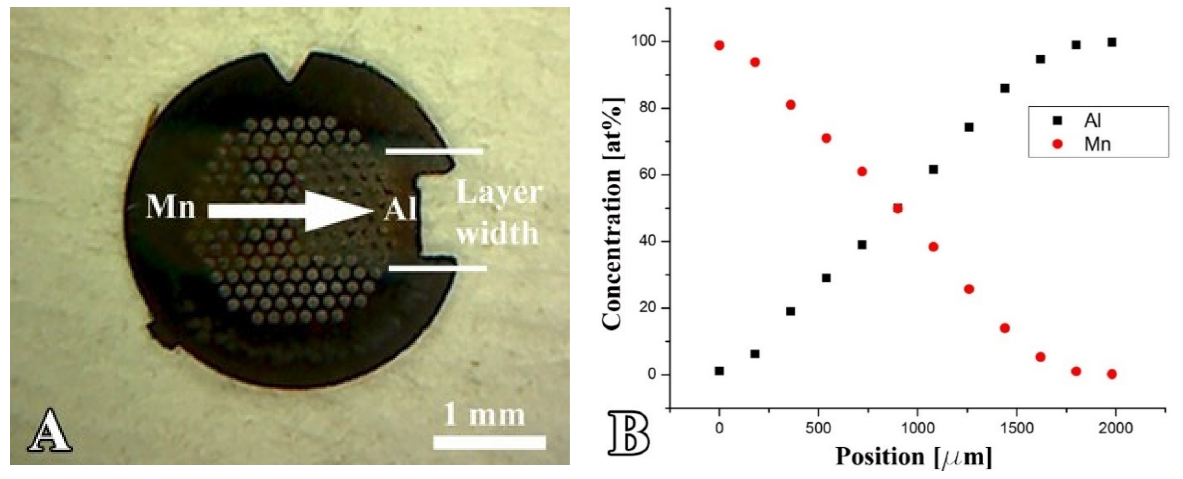
Figure 1. (A) Thin Mn–Al micro-combinatorial sample deposited on a Mo TEM grid via dual DC magnetron sputtering. The 1 mm wide layer strip consists of a 1.5 mm long gradient Mn–Al section enclosed by 0.25 mm long pure Mn and pure Al sections. (B) Mn and Al concentration profiles measured by EDS as a function of the position along the TEM grid shown in “A”.
The concentration gradient section at the center of the Mn-Al strip was 1.5 mm long and surrounded by 0.25 mm of pure Mn and pure Al. The concentration gradient under the experimental conditions was 0.067 at%/µm. After the deposition of the combinatorial sample, a thin SiOx protective layer was applied to prevent oxidation of the sample. The experimental conditions and details of the deposition process were published in [7]. The sample was characterized in a 200 kV Philips CM20 TEM by bright and dark field imaging, Selected Area Electron Diffraction (SAED), and Energy-Dispersive X-ray Spectrometry (EDS). Figure 1. illustrates that the morphology and structure of the AlMn binary layer system can be revealed over the entire composition range by measuring a single sample.
Figure 1A shows the photo of a MnAl combinatorial sample on a Mo TEM grid. The length of the arrow (1.5 mm) corresponds to the length of the gradient section. The elemental distribution along the sample measured by EDS is shown in Figure 1B. The Mn and Al concentration profiles are acceptably linear as a function of the position. However, at the boundaries between the one- and two-component regions, the profiles are curved because the width of the gap used to distribute the deposited layer is not zero. This is a minor disadvantage because the composition can be checked by EDS at any place as well as within the curved sections.
The TEM micrographs and SAED insets in Figure 2a–c show the typical morphology and structure of the µ-combinatorial sample at selected compositions. The films of 90 at%Mn in (a) present a fine-grained cubic Mn phase with some cubic MnO. This microstructure persists, while the Mn content decreases from 100% to about 50%. The 50–10%Mn concentration range is characterized by the presence of an amorphous MnAl phase, which is represented in (b) by the 40%Mn layer. Next to the amorphous phase, at 20%Mn and below, an fcc Al phase appears with a relatively large grain size. The grain size continues to increase, and the fcc Al phase becomes more prevalent as the Mn content decreases to 0%Mn.
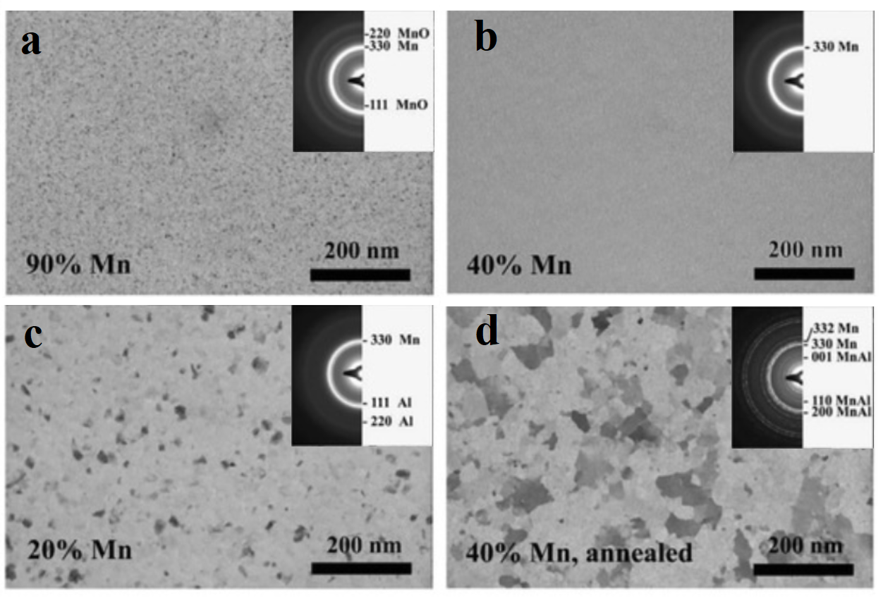
Figure 2. TEM micrographs of a Mn–Al µ-combinatorial sample at (a) 90%, (b) 40%, and (c) 20%Mn concentrations showing fine-grained cubic Mn with Mn oxide, amorphous MnAl, and amorphous MnAl with an fcc Al phase, respectively. The layer depicted in (d) is that of 40%Mn after heat treatment at 500 °C/0.5 h in Ar–H2 mixture showing tetragonal MnAl phase. The insets are SAED patterns and DF images.
Note that in addition to the phases of the layers deposited at room temperature, all the MnAl phases formed at an elevated temperature can be studied after the annealing of the deposited µ-combinatorial sample. For example, the 40%-Mn-containing film after annealing in a 500 °C/0.5 h Ar–H2 mixture (Figure 2d) shows a tetragonal Mn 14 Al 11 phase (Pdf 11-0520) identified by the appearance of 001, 110, and 200 rings in SAED. However, a detailed analysis of the heat-treated layers is outside the scope of this work. It should also be emphasized that both theoretical calculations and experimental results show that the diffusion effect between the adjacent film areas with different compositions is negligible.
Figure 3 shows the phases found in the as-deposited μ-combinatorial TEM sample via SAED intensity distribution plots as a function of an Al-Mn elemental composition. From the bottom to the top of the figure, the microstructural changes associated with decreasing Mn concentrations can be clearly followed (as could be seen in the selected examples in the previous Figure 2a–c). At 100%, 80%, and 60% manganese content, the sample is characterized by a fine-grained cubic α-Mn phase (Pdf 32-0637) with broad 222, 330, and 332 peaks and 111 and 220 peaks of cubic MnO (Pdf 75-0621) [8]. With 60%Mn content, the 330 peak becomes broader, i.e., more diffuse, which represents a continuous grain-size reduction. A further decrease in Mn concentration leads to amorphization. When the Mn content is reduced to 40%, an amorphous Mn(Al) solid solution is obtained. At the same time, the two peaks of the MnO phase disappear, presumably because the layer with a higher Al concentration is less sensitive to oxidation. Intensity diagrams for the 20%, 10%, and 0%Mn concentrations show a gradual decrease in the peak of the amorphous Mn(Al) solid solution and an increase in peaks identified with the 111, 200, and 220 reflections, showing the co-presence of an amorphous Mn(Al) phases and a crystalline fcc Al phase. The latter consists of Al grains of increasing size as the Al concentration increases. When the Mn concentration reaches 0%, i.e., 100%Al, the layer consists of an entirely fcc Al phase.
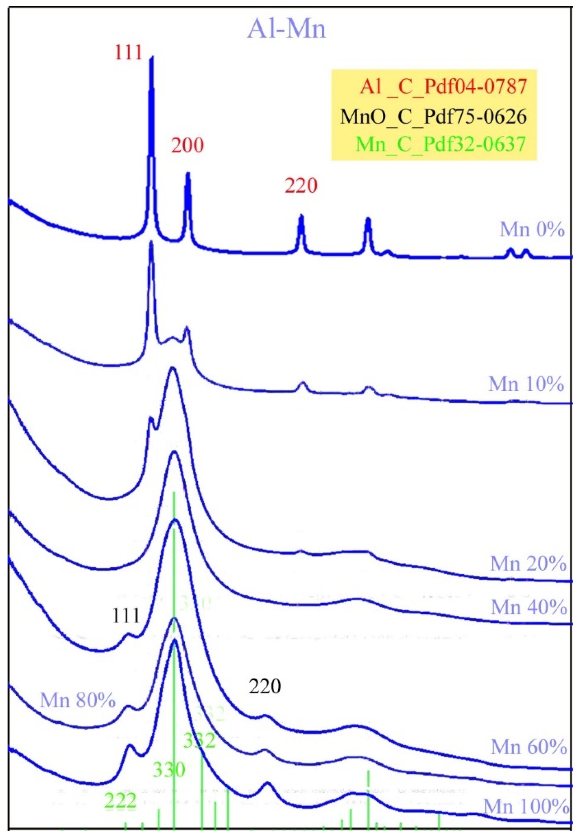
Figure 3. SAED intensity distributions representing the phases of the AlMn layer depicted in Figure 2 with various compositions obtained from a single µ-combinatorial TEM sample deposited at room temperature. Green, black, and red indices show the peak positions of cubic Mn, MnO, and Al phases, respectively.
2.2. Al-Mg Films from Submicron Grain Size to Amorphous Structure
Due to their excellent mechanical properties, aluminum alloys in bulk form are indispensable materials in the automotive, construction, and aerospace industries and are, therefore, the focus of research [9][10].
The new micro-combinatorial method [11] has been used to effectively reveal the correlations between the structure and mechanical properties of thin Al-Mg films. This flexible method allows for the preparation of samples that meet the requirements of relevant measurement techniques. To characterize structure and morphology by TEM, a thin concentration gradient sample covering the entire compositional range was deposited on a TEM grid. To measure mechanical properties by nanoindentation [12], a series of 2 × 12 mm2 strips of selected discrete compositions were deposited on a single Si substrate in one experimental run to cover the technologically relevant composition range of an AlMg system (0–30 at%Mg) [11].
The TEM images in Figure 4a–d show the microstructures of the films at 0, 1, 10, and 30%Mg content, respectively. The fine grain size (~110 nm) of pure Al (0%Mg) shown in (a) decreases further when increasing the Mg concentration (~80 nm for 1%Mg), reaching ~40 nm for Al-10at%Mg (c). Finally, the layer appears dominantly amorphous at Al-30at%Mg (d). According to the SAED results, the layers exhibit an fcc Al(Mg) phase at each composition up to 30%Mg.
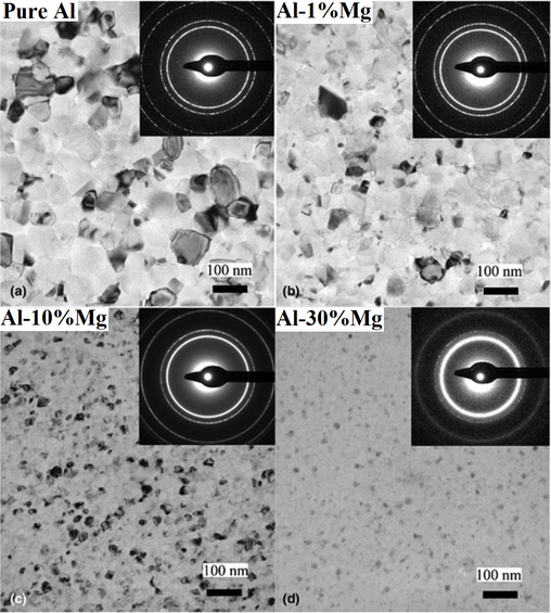
Figure 4. TEM images with SAED insets of (a) pure Al, (b) Al–1%Mg, (c) Al–10%Mg, and (d) Al–30%Mg films, showing microstructures with very fine grain sizes decreasing with an increasing Mg content. The films exhibit fcc Al(Mg) phase at each composition up to 30%Mg, at which point an amorphous component becomes dominant.
The nanoindentation measurements were performed on distinct strips prepared with selected compositions [11]. Figure 5 shows the indentation depth–load (h–F) curves of the AlMg layers at 0, 1, 5, 10, and 30%Mg concentrations. It is evident that as low as a 1 at%Mg level of alloying leads to a remarkable decrease in the penetration depth of the indenter, i.e., a significant (~3×) hardness increase compared to pure Al. The nano-hardness (H) of the layers plotted against the Mg concentration in Figure 6 shows a further increase, reaching the remarkable high value of Hmax = 8 GPa at an about 15 at%Mg concentration.
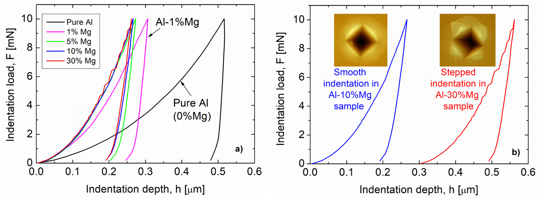
Figure 5. Indentation depth–load (h–F) curves of (a) the samples of various Al–Mg compositions and (b) of the Al–10%Mg and Al–30%Mg samples together with the corresponding AFM images regarding the indented surface (the h–F curve of the sample Al–30%Mg sample is shifted to the right by 0.5 μm for clarity).

In the case of the Al-30%Mg film shown in Figure 5b, an interesting phenomenon, namely, a stepped behavior of the penetration curve, was observed. This is in complete agreement with both the dominant amorphous structure determined by TEM and SAED (Figure 4d) and with the appearance of deformation bands around the imprint as revealed by AFM (Figure 5b). Indeed, the discontinuous indentation curve is a phenomenon typical of the deformation of amorphous materials [13].
2.3. High Strength in AlCu Thin Films
Among their other advantageous mechanical properties, bulk AlCu alloys are also known for their special aging behavior [14], which has been well studied and documented [15]. However, in the form of thin films, this special alloy is hardly discussed and only in cases with low Cu concentrations [16][17]. To study the structural and mechanical properties of the AlCu thin film system in a wide compositional range, Draissia et al. [18][19] deposited several thin film samples using cathodic radiofrequency (RF) sputtering. They used composite targets in which a bulk Cu disk was inserted into a bulk Al ring, and by changing the surface fraction of the insert, the composition of the sputtered layer was adjusted. Through their method, 10 different, separate samples with Cu concentrations ranging from 1.8 to 92.5 at% were prepared [19]. The microstructural characteristics were determined by XRD and TEM, while the hardness of the layers was determined by nanoindentation.
Recently, the micro-combinatorial method has been applied to the structural and mechanical investigation of the AlCu thin film system [20], which has allowed for a more efficient and reproducible characterization over the whole concentration range compared to the traditional one-experiment–one-sample method. In a single vacuum cycle experiment using dual DC magnetron sputtering, 15 distinct strips of films with dimensions of 12 × 1 mm2 that were ~1.7 um thick and had different Al-Cu compositions were deposited abreast on a 12 × 25 mm2 Si substrate. The Cu-alloying concentrations in the strips were chosen to cover the whole range from 0 at% to 100 at%, thus providing a comprehensive study of the whole AlCu layer system. The micro-combinatorial method allowed for the preparation of all 15 layers in one vacuum cycle and in one experiment. It ensured identical sputtering conditions for the strips in the UHV vacuum chamber, e.g., residual and Ar working gas pressures, and with regard to the type and amount of impurities in the system; these are key parameters for reproducibility, as they can significantly affect the properties of a coating [21]. This sample design greatly aided the determination of the system’s mechanical properties via nanoindentation measurements. As a result, Figure 7 shows the evolution of the nano-hardness of the AlCu thin film system as a function of both Cu concentration and max. indentation load. In this layer system, two unexpected phenomena were found: at a concentration of 52 at%Cu, an exceptionally high strength of ~16 GPa was observed, approaching or even reaching the strength of some industrial protective coatings [22].
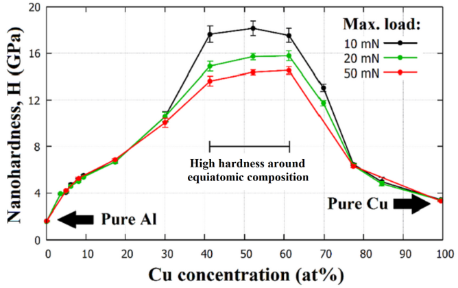
In addition to high hardness, Figure 7 represents another phenomenon, namely, that at low alloying concentrations, indentations at 10, 20, and 50 mN result in identical H values, while in the intermediate range at ~40–70 at%Cu, lower maximum indentation forces are coupled with higher H values. This interesting phenomenon is called the indentation size effect (ISE), where smaller indentation traces (smaller maximal indentation forces) are associated with higher hardness values for the material. The ISE makes it very difficult to compare the results of hardness measurements taken at different loads. There is a widely accepted theory developed by Nix and Gao [23] that uses geometrically necessary dislocations (GNDs) for the explanation of these phenomena; unfortunately, there is still some uncertainty about its origin, as many factors can have an influence on the determination of hardness, such as the friction between the indenter tip and the indented material [24] or imperfections of the indenter tip [25].
From the comparison of the microstructures of the layers (not shown here) with and without ISE, the otherwise surprising lack of an indentation size effect in the pure Al and pure Cu layers [20] could be attributed to the predominance of the sliding deformation mechanism of the grain boundaries [26].
Thus, it can be concluded that the micro-combinatorial technique has allowed for sampling with a planned, suitable concentration resolution for a comprehensive characterization of binary layer systems. As a result, two phenomena have been discovered and interpreted, namely, the extreme hardness of a binary alloy layer containing rather soft constituents (Al and Cu) and the indentation size effect (ISE).
2.4. a-SiGe and Hydrogenated a-SiGe Combinatorial Thin Films
The research of thin, amorphous (a-) SiGe and hydrogenated a-SiGe (a-SiGe:H) films is motivated by their technological importance and wide range of applications in solar cells [27][28][29][30], thin film transistors [31][32], Schottky diodes [33][34], thermal sensors [35], bolometers, etc. SiGe-on-Si is of particular interest because varying the Ge concentration of this alloy allows for the fine tuning of material properties such as bandwidth or the refractive index. In the SiGe system, the operating range can be extended by up to 8 μm (the wavelength of the onset of Si absorption) and further extended up to 14 μm (Ge transparency cut-off wavelength) for devices with a low Si concentration [36][37][38].
In this section, it is shown that the micro-combinatorial method has proven to be a very effective technique for the efficient investigation of the structural and optical properties of SiGe and SiGe:H layer systems. This has been demonstrated both in the preparation of a single sample containing a complete binary layer system and by providing optimal conditions for a very efficient characterization of the sample through a range of analytical techniques [39][40] (as shown in Figure 8). While the original procedure [7] of depositing a 1 mm concentration-gradient-length film on a 3 mm diameter grid (Figure 8a) was adequate for TEM studies, to determine optical properties, the sample had to be enlarged to approximately 1 × 0.5 inches, which is in line with the smallest focal spot size (~0.3 mm) typically available for spectroscopic ellipsometry (SE) [41] measurements. Figure 8b shows a schematic of the composition-spread SiGe layer on the 10 × 25 mm2 Si substrate, spanning a 20 mm gradient region in the center of the sample. SiGe films were prepared by dual DC sputtering of Si and Ge targets in an Ar atmosphere, while SiGe:H samples were sputtered in a mixture of high-purity H and Ar at pH/p = 0, 0.05, 0.10, and 0.20 H partial pressures. For the detailed description of the experimental procedure, see Ref [39][40]. The excellent reliability of the micro-combinatorial method for achieving the desired concentration profile is illustrated in Figure 8d, which shows a very well-matched linear variation of the Si and Ge atomic concentrations along the substrate through two independent methods: Rutherford Backscattering Spectrometry (RBS) and Energy Dispersive X-ray Spectrometry (EDS). The RBS result is indicated by a solid line (red for Si and blue for Ge), and the result of EDS is plotted with a dashed line (only the variation of Si is shown).

Figure 8. SixGe1-x (0 ≤ x ≤ 1) thin films fabricated via the micro-combinatorial method (a) on a Mo grid for TEM measurements. (b) A schematic of the sample for spectroscopic ellipsometry investigations. (c) The compositional change across the TEM grid obtained by TEM EDS and (d) along the 10 × 25 mm2 Si slab obtained via RBS (continuous line) and EDS (dashed line).
It was revealed that the hydrogen content of the layer of the hydrogenated SiGe:H samples also varies linearly with the sample’s position, i.e., the concentration of Si as detailed in [39][40].
Figure 9 shows the color-coded maps of the extinction coefficient (k) and the refractive index (n) values revealed for the amorphous hydrogenated SiGe films prepared at PH/Psputt = 0, 0.05, 0.1, and 0.2 H partial pressures as a function of photon energy and position along the sample. It can be observed that both k and n show a linearly dependent behavior with respect to the position, i.e. the Si-Ge composition.
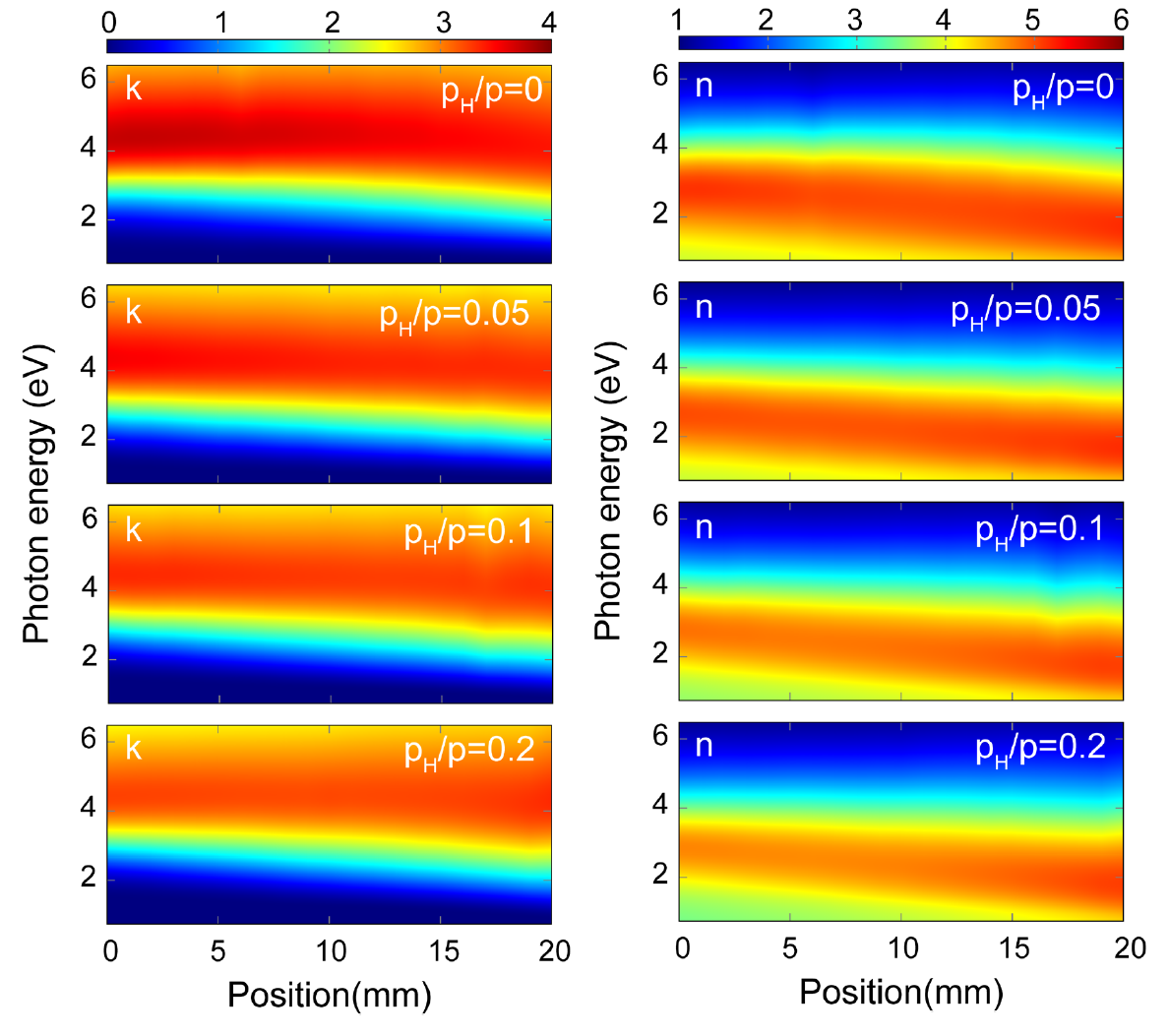
Figure 9. Color-coded maps of the extinction coefficient k (left) and the refractive index n (right) of hydrogenated amorphous SiGe films prepared at different H partial pressures (PH/Psputt = 0, 0.05, 0.1, and 0.2) as a function of position and photon energy measured by ellipsometry on micro-combinatorial samples. The 0 mm and 20 mm positions correspond to the pure Si and pure Ge ends of the sample with linearly varying composition.
These maps represent a library of optical properties of the hydrogenated amorphous SiGe: H system, covering the full range of Si-Ge compositions as well as a wide range of hydrogen concentrations and photon energy. This color-coded library and its tabular representation with numerical data [40] can be a very useful reference database for researchers and technologists working with the amorphous silicon-germanium system.
2.5. Reactively Sputtered Combinatorial Si-O-N Layer system
Pure silicon dioxide (SiO2 ) and nitride (SiNx) are well-known essential materials in electronic technology and are produced using a series of production techniques [42][43]. In its complex form, amorphous, ternary silicon oxynitride (SiON) is a chemically stable material. Depending on the oxygen and nitrogen content it shows a refractive index between 1.45 and 2.05 that would provide wide application range in optoelectronics. However, this layer system is hardly used due to technological difficulties wherein the composition of the SiON and thus its refractive index are particularly sensitive to small changes in sputtering parameters, especially oxygen content of the plasma gas [44]. This evokes a strong motivation to investigate the sputtering process itself and reveal the correlations between the sputtering conditions, composition, and optical properties of the Si-O-N thin film system over the whole composition range.
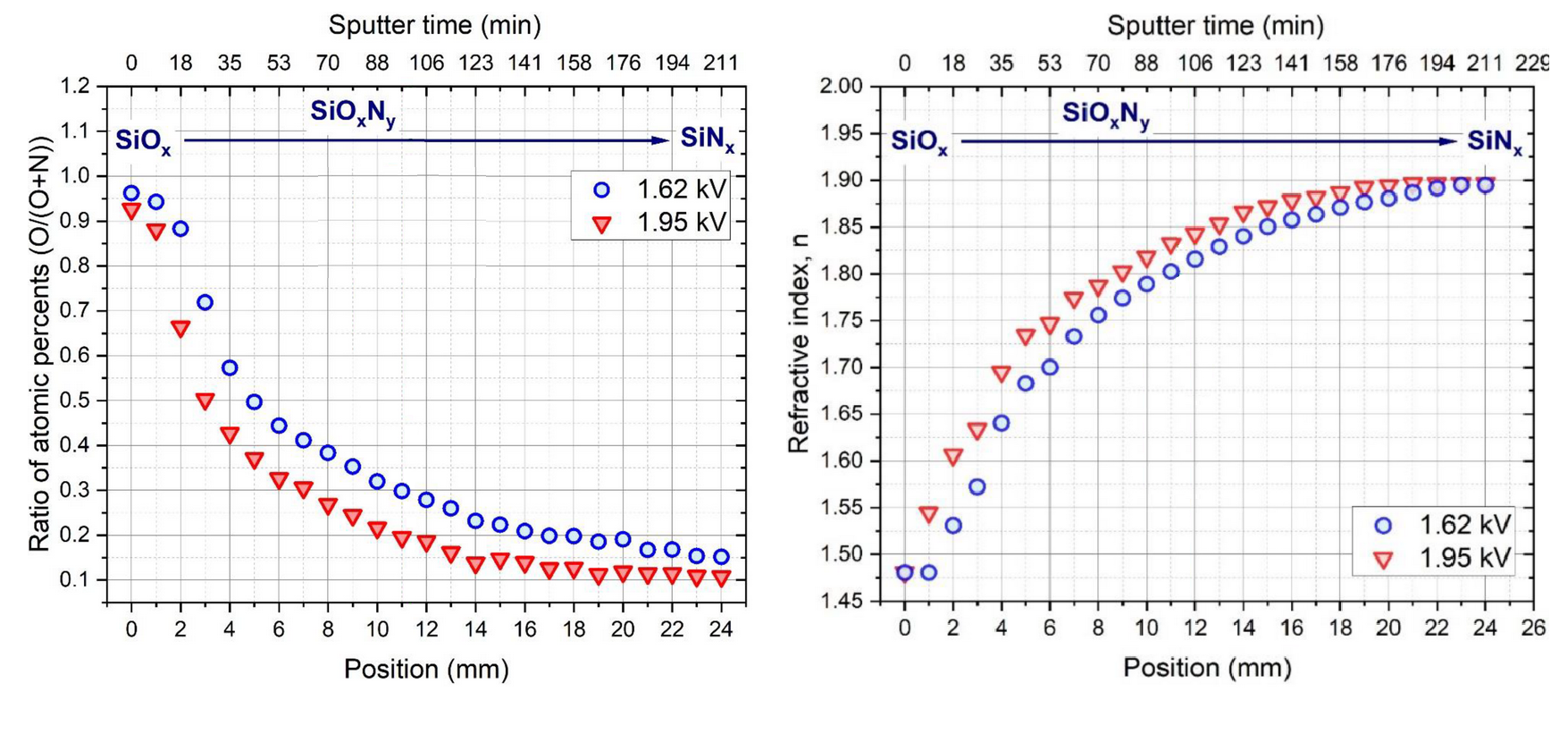
Figure 10. (Left): Atomic concentrations (O/O+N) measured by SEM EDS along the micro-combinatorial SiON samples deposited at 1.62 and 1.95 kV wall potentials. A continuous decrease in the O content was observed, resulting in SiOx à SiOxNy à SiNx transitions. (Right): corresponding SE results showing the variation of the refractive index, n as a function of position, i.e. composition.
The influence of a variable reactive gas inlet during RF sputter deposition of Si-O-N, the use of the micro-combinatorial layer growth method, and the correlations found between the sputtering parameters, layer composition, and refractive index, are plotted in the diagrams in Figure 10. and serve as a base of a model for the sputtering process detailed in [45].
3. Summary
The novel micro-combinatorial technique allows for a high-throughput comprehensive characterization of the structure and material properties of multicomponent thin film systems, revealing their interrelationships and determining their underlying mechanisms. This materials characterization technique has proven to be extremely effective in producing and testing complete two- and three-component layer systems of variable compositions within a single sample, adapted to the analytical method used. The scientific results already achieved, as well as the innovation potential of the high-throughput concept, including the creation of two- and three-component thin film databases, can be well exploited in research, technology, and applications.
References
- Encyclopedia Britannica. Available online: https://www.britannica.com/science/combinatorics (accessed on 12 February 2023).
- Dorfman, R. The Detection of Defective Members of Large Populations. Ann. Math. Statist. 1943, 14, 436–440.
- Kōno, H. On the Ferromagnetic Phase in Manganese-Aluminum System. J. Phys. Soc. Jpn. 1958, 13, 1444–1451.
- Jiménez-Villacorta, F.; Marion, J.L.; Sepehrifar, T.; Daniil, M.; Willard, M.A.; Lewis, L.H. Exchange anisotropy in the nanostructured MnAl system. Appl. Phys. Lett. 2012, 100, 112408-1–112408-4.
- Sáfrán, G.; Szívós, J.; Németh, M.; Horváth, A. Phase Mapping of thin Mn-Al layers by combinatorial TEM. In Proceedings of the 12th Multinational Congress on Microscopy: MCM 2015 Budapest, Eger, Hungary, 23–28 August 2015; Akadémiai Kiadó: Budapest, Magyarország; p. 599.
- Sáfrán, G. A microcombinatorial TEM method for phase mapping of thin two-component films. In European Microscopy Congress 2016: Proceeding; Wiley-VCH Verlag: Lyon, France, 2016; pp. 483–484.
- Sáfrán, G. “One-sample concept” micro-combinatory for high throughput TEM of binary films. Ultramicroscopy 2018, 187, 50–55.
- PCPDFWIN Powder Diffraction Files Ver. 2.01, November 1998. Available online: https://instanano.com/xrd-analysis-online/ (accessed on 23 February 2023).
- Benedyk, J.C. Aluminum alloys for lightweight automotive structures. In Materials, Design and Manufacturing for Lightweight Vehicles; Woodhead Publishing: Cambridge, UK, 2010; pp. 79–113.
- Miller, W.S.; Zhuang, L.; Bottema, J.; Witterbrood, A.J.; De Smet, P.; Haszler, A.; Vieregge, A. Recent development in aluminium alloys for the automotive industry. Mater. Sci. Eng. A 2000, 280, 37–49.
- Chinh, N.Q.; Sáfrán, G. High strength of ultrafine-grained Al-Mg films and the relevance of the modified Hall-Petch-type relationship. MRS Commun. 2019, 9, 1111–1114.
- Olasz, D.; Lendvai, J.; Szállás, A.; Gulyás, G.; Chinh, N.Q. Extended Applications of the Depth-Sensing Indentation Method. Micromachines 2020, 11, 1023.
- Schuh, C.A.; Nieh, T.G. A nanoindentation study of serrated flow in bulk metallic glasses. Acta Mater. 2003, 51, 87–99.
- Guinier, A. Structure of Age-Hardened Aluminium-Copper Alloys. Nature 1938, 142, 569–570.
- Rathod, N.R.; Menghani, J.V. Influence of precipitation hardening in aluminum based systems: A literature review. AIP Conf. Proc. 2021, 2317, 020035-1–020035-11.
- Joo, Y. Mechanical properties and microstructure of Al-Cu thin films with various heat treatments. Met. Mater. 1998, 4, 1033–1039.
- Bergers, L.J.C.; De Hosson, J.T.M.; Geers, M.G.D.; Hoefnagels, J.P.M. Anomalous precipitation hardening in Al-(1 wt%)Cu thin films. Mater. Sci. Eng. A 2018, 722, 37–46.
- Draissia, M.; Boudemgh, H.; Debili, M.Y. Structure and hardness of the sputtered Al-Cu thin films system. Phys. Scr. 2004, 69, 348–350.
- Draissia, M.; Debili, M.Y. Strengthening of nanostructured aluminium-copper thin films. J. Metastable Nanocryst. Mater. 2004, 22, 121–126.
- Olasz, D.; Sáfrán, G.; Szász, N.; Huhn, G.; Chinh, N.Q. Indentation size effect in exceptionally hard AlCu thin films. Mater. Lett. 2023, 330, 133409.
- Behravan, N.; Farhadizadeh, A.; Ghasemi, S.; Khademi, A.; Shojaei, H.; Ghomi, H. The pressure dependence of structure and composition of sputtered AlCrSiTiMoO high entropy thin film. J. Alloy. Compd. 2021, 852, 156421.
- Pujada, B.R.; Tichelaar, F.D.; Janssen, G.C.A.M. Hardness of and stress in tungsten carbide-diamond like carbon multilayer coatings. Surf. Coat. Technol. 2008, 203, 562–565.
- Nix, W.D.; Gao, H. Indentation size effect in crystalline materials: A law for strain gradient plasticity. J. Mech. Phys. Solids 1998, 46, 411–425.
- Atkinson, M. Further analysis of the size effect in indentation hardness tests of some metals. J. Mater. Res. 1995, 10, 2908–2915.
- Menčík, J.; Swain, M.V. Errors associated with depth-sensing microindentation tests. J. Mater. Res. 1995, 10, 1491–1501.
- Chinh, N.Q.; Szommer, P.; Horita, Z.; Langdon, T.G. Experimental evidence for grain-boundary sliding in ultrafine-grained aluminum processed by severe plastic deformation. Adv. Mater. 2005, 18, 34–39.
- Yang, J.; Banerjee, A.; Guha, S. Triple-junction amorphous silicon alloy solar cell with 14.6% initial and 13.0% stable conversion efficiencies. Appl. Phys. Lett. 1997, 70, 2975–2977.
- Deng, X.; Liao, X.; Han, S.; Povolny, H.; Agarwal, P. Amorphous silicon and silicon germanium materials for high-efficiency triple-junction solar cells. Sol. Energy Mater. Sol. Cells 2000, 62, 89–95.
- Yang, J.; Banerjee, A.; Guha, S. Amorphous silicon based photovoltaics—From earth to the “final frontier”. Sol. Energy Mater. Sol. Cells 2003, 78, 597–612.
- Yue, G.; Yan, B.; Teplin, C.; Yang, J.; Guha, S. Optimization and characterization of i/p buffer layer in hydrogenated nanocrystalline silicon solar cells. J. Non-Cryst. Solids 2008, 354, 2440–2444.
- Engwall, J.; Nagesh, V.; Grimmeiss, H.G. Electrical characterization of Si-Ge heterostructure bipolar transistors. Thin Solid Film. 1992, 222, 154–156.
- Gribelyuk, M.A.; Fu, B.; Zhao, W.W. Measurement of SiGe composition in 3-D semiconductor Fin Field Effect Transistor devices. J. Appl. Phys. 2019, 125, 165306-1–165306-9.
- Haller, E.E. Germanium: From its discovery to SiGe devices. Mater. Sci. Semicond. Process. 2006, 9, 408–422.
- Pfeiffer, U.R.; Mishra, C.; Rassel, R.M.; Pinkett, S.; Reynolds, S.K. Schottky Barrier Diode Circuits in Silicon for Future Millimeter-Wave and Terahertz Applications. IEEE Trans. Microw. Theory Tech. 2008, 56, 364–371.
- Cojocaru, A.; Carstensen, J.; Boor, J.D.; Kim, D.S.; Schmidt, V.; Föll, H. Production and Investigation of Porous Si-Ge Structures for Thermoelectric Application. ECS Trans. 2011, 33, 193–202.
- Ramirez, J.M.; Vakarin, V.; Frigerio, J.; Chaisakul, P.; Chrastina, D.; Le Roux, X.; Ballabio, A.; Vivien, L.; Isella, G.; Marris-Morini, D. Ge-rich graded-index Si1-xGex waveguides with broadband tight mode confinement and flat anomalous dispersion for nonlinear mid-infrared photonics. Opt. Express 2017, 25, 6561–6567.
- Humlíček, J.; Garrira, M.; Alonso, M.I.; Cardona, M. Optical spectra of SixGe1-x alloys. J. Appl. Phys. 1989, 65, 2827–2832.
- Brun, M.; Labeye, P.; Grand, G.; Hartmann, J.; Boulila, F.; Carras, M.; Nicoletti, S. Low loss SiGe graded index waveguides for mid-IR applications. Opt. Express 2014, 22, 508–518.
- Lohner, T.; Kalas, B.; Petrik, P.; Zolnai, Z.; Serényi, M.; Sáfrán, G. Refractive Index Variation of Magnetron-Sputtered a-Si1-xGex by “One-Sample Concept” Combinatory. Appl. Sci. 2018, 8, 826.
- Kalas, B.; Zolnai, Z.; Sáfrán, G.; Serényi, M.; Agócs, E.; Lohner, T.; Németh, A.; Khánh, N.Q.; Fried, M.; Petrik, P. Micro-combinatorial sampling of the optical properties of hydrogenated amorphous Si1-xGex for the entire range of compositions towards a database for optoelectronics. Sci. Rep. 2020, 10, 19266.
- Aspnes, D.E. Spectroscopic ellipsometry—Past, present, future. Thin Solid Film. 2014, 571, 334–344.
- Shi, Y.; He, L.; Guang, F.; Li, L.; Xin, Z.; Liu, R. A review: Preparation, Performance, and Applications of Silicon Oxynitride Film. Micromachines 2019, 10, 552.
- Merziani, S.; Moussi, A.; Mahiou, L.; Outemzabet, R. Compositional analysis of silicon oxide/silicon nitride thin films. Mater. Sci. Pol. 2016, 34, 315–321.
- Serényi, M.; Rácz, M.; Lohner, T. Refractive index of sputtered silicon oxynitride layers for antireflection coating. Vacuum 2001, 61, 245–249.
- Hegedűs, N.; Balázsi, C.; Kolonits, T.; Olasz, D.; Sáfrán, G.; Serényi, M.; Balázsi, K. Investigation of the RF Sputtering Process and the Properties of Deposited Silicon Oxynitride Layers under Varying Reactive Gas Conditions. Materials 2022, 15, 6313.

