Your browser does not fully support modern features. Please upgrade for a smoother experience.
Submitted Successfully!
 +1 credit
Thank you for your contribution! You can also upload a video entry or images related to this topic.
For video creation, please contact our Academic Video Service.
| Version | Summary | Created by | Modification | Content Size | Created at | Operation |
|---|---|---|---|---|---|---|
| 1 | Yajun Pang | -- | 3762 | 2023-07-06 12:28:28 | | | |
| 2 | Jessie Wu | Meta information modification | 3762 | 2023-07-07 03:47:48 | | |
Video Upload Options
We provide professional Academic Video Service to translate complex research into visually appealing presentations. Would you like to try it?
Cite
If you have any further questions, please contact Encyclopedia Editorial Office.
Hu, M.; Pang, Y.; Gao, L. Silicon-Based Optical Phased Array Lidar. Encyclopedia. Available online: https://encyclopedia.pub/entry/46517 (accessed on 22 July 2026).
Hu M, Pang Y, Gao L. Silicon-Based Optical Phased Array Lidar. Encyclopedia. Available at: https://encyclopedia.pub/entry/46517. Accessed July 22, 2026.
Hu, Mingxuan, Yajun Pang, Long Gao. "Silicon-Based Optical Phased Array Lidar" Encyclopedia, https://encyclopedia.pub/entry/46517 (accessed July 22, 2026).
Hu, M., Pang, Y., & Gao, L. (2023, July 06). Silicon-Based Optical Phased Array Lidar. In Encyclopedia. https://encyclopedia.pub/entry/46517
Hu, Mingxuan, et al. "Silicon-Based Optical Phased Array Lidar." Encyclopedia. Web. 06 July, 2023.
Copy Citation
Silicon-based Lidar is an ideal way to reduce the volume of the Lidar and realize monolithic integration. It removes the moving parts in the conventional device and realizes solid-state beam steering. The advantages of low cost, small size, and high beam steering speed have attracted the attention of many researchers.
silicon-based Lidar
OPA Lidar
optical switch Lidar
power
1. Introduction
Mechanical Lidar is often limited in performance and cost due to mechanical beam orientation and stabilization mechanisms. In order to achieve random pointing and stable scanning results, the Lidar needs to rotate precisely and quickly, leading to high power consumption. To solve this problem, researchers proposed a Silicon-based optical phased array Lidar with low power consumption and a stable working state. The principle of the optical phased array is similar to that of the microwave phased array. The direction of the main beam can be changed by controlling the phase difference between the beams. The Lidar formed by an optical phased array completely gets rid of mechanical components.
An optical phased array is usually composed of a coherent light source, beam splitter, phase shifters, and optical antennas [1]. The light source is divided into multiple waveguides by the splitter, then modulated by the phase shifters and transmitted to the free space by the grating couples. The time taken for the light to reach the equiphase surface is the same when the phase of each ray is the same. Suppose there is a uniform phase difference between two adjacent paths. In that case, the equiphase surface is no longer perpendicular to the direction of the original path but produces a beam deflection angle. According to the knowledge of optical interference, the optical path of the equal phase will be longer than that of the coherent phase, and the optical path of the unequal phase will cancel each other. Therefore, the final synthesized wavefront forms a certain angle with the propagation direction of the original optical path [2].
Usually, 2D beam steering can be achieved in two ways as shown in Figure 1: (a) in a one-dimensional optical phased array, the beam steering is accomplished by wavelength tuning in the longitudinal direction, θ, and phase shifting in the lateral, φ. The phase difference between adjacent grating couplers is ϕ; (b) in a two-dimensional optical phased array, the deflection of the beam in both directions is realized by phase delay. Some parameters of the OPA Lidar have been listed in Table 1.
Figure 1. Schematic of optical phased array Lidar. (a) Optical steering in the longitudinal direction (θ) and lateral direction (φ) by 1D OPA. (b) Optical steering in directions by 2D OPA. (c) The emitted waves with no phase delay. (d) The emitted waves with phase delay [1].
Table 1. The parameters of the OPA Lidar in this section.
| Reference | FoV (Degree) |
Beam Width (Degree) |
Platform Materials |
New Finding (s) |
Wavelength (nm) |
|---|---|---|---|---|---|
| [3] | 0~3 | 0.25 | SOI | irregular phased array |
1550 |
| [4] | 2.3 × 14.1 | - | SOI | thermo-optical and wavelength tuning | 1550 |
| [5] | - | - | SOI | high wavelength steering low antenna loss |
1550 |
| [6] | 20 × 14 | <1 | SOI | Small phase error and background peak noise | 1500 1550 1600 |
| [7] | 31.9 | - | SOI | silicon nanomembrane with off-chip laser source |
1550 |
| [8] | 23 | 1.27 | SOI | waveguides of special structure to minimize the damage in sharp turns | 1550 |
| [9] | 15 × 50 | 4.0 | SOI | high steering efficiency | 1500–1600 |
| [10] | 51 | - | SOI | high speed beam steering |
1550 |
| [11] | 46 × 36 | - | SOI | utilize grouped cascaded phase shifters | 1550 |
| [12] | 80 × 17 | 0.14 | SOI | high resolution and wide beam steering angle | 1260–1360 |
| [13] | 56 × 15 | - | SOI | low power consumption and high directivity |
1450–1640 |
| [14] | 18.5 | 0.15 | SOI | the first Lidar system based on OPA | 1550 |
| [15] | 70 × 6 | - | SOI | cycle the light to achieve phase shifting | 1525–1600 |
| [16] | 54.5 × 77.8 | - | SOI | the bi-directional OPA with only one grating antenna array |
1500–1600 |
| [17] | - | 0.089 | SiN-Si | a solution to solve the trade-off between FoV and beam divergence | 1550 |
| [18] | 51 × 28 | 0.02 | hybrid III-V/Si waveguides | wide optical bandwidth high operating speed(1 GHz) |
1550 |
| [19] | 48 × 14 | - | SiN-Si | an ideal way to long range detection |
1550 |
| [20] | 12 × 30 | - | silicon nitride mixed polymer | high thermal and optical effect |
- |
| [21] | 96 × 14.4 | 1.9 | SiN-Si | power processing capacity high thermal-optical modulation efficiency |
1550 |
2. OPA Lidar Based on Silicon on Insulator
As early as 1997, P. Trinh et al., University of California, produced the first four-channel wavelength multiplexer fabricated in the silicon-on-insulator [22]. The channel interval of the wavelength multiplexer was 1.9 nm, the crosstalk of the adjacent channel was less than −22 dB, the on-chip insertion loss of the channel was less than 6 dB, and the TE-TM shift was less than 0.04 nm, which reached the minimum polarization displacement in the waveguide circuit without compensation technology at that time. However, the scanning angle is limited to the chip plane.
In 2005, F. Xiao et al. theoretically proposed a non-uniform phased array [23] to control the beam by changing the wavelength. This method can effectively suppress the side lobe and reduce the difficulty of producing and controlling. After two years, F. Xiao et al. presented the theory of a cascaded irregular phased array [24]. They calculated the relationship between the device size and spacing in each array stage and realized the beam’s phase matching at the two-stage cascade. Based on the above simulation and theory, this research group produced 16- and 32-element irregular phased arrays on silicon-on-insulator materials in 2008 [3]. The device consists of irregular elements that allow a continuous sweep range of 0° to 3° when the wavelength varies from 1550.7 nm to 1551.9 nm.
In 2009, K. Van Acoleyen et al., from the University of Ghent reported a one-dimensional optical phased array composed of 16 grating couplers spaced 2 μm apart [4], as shown in Figure 2. At a wavelength of 1550 nm, it can achieve continuous thermo-optical steering of 2.3° and wavelength steering of 14.1°. However, considering that excessive current will destroy electronic devices in actual use, the current is limited to 3.95 mA, so the transverse scanning range is also limited.
Figure 2. The optical phased array consists of 16 parallel grating couplers spaced 2 μm apart. θ: outcoupling angle along the waveguide axis. ψ: outcoupling angle perpendicular to the waveguide axis. The inset shows the far-field image [4].
K. Van Acoleyen et al. reported a two-dimensional optical phased array fabricated on SOI in 2010 [5]. The input waveguide is connected to a grating coupler which couples light into the system. This grating coupler uses the diffraction principle to couple the light from a single-mode fiber into the TE-like mode of a 10 μm waveguide, and then the waveguide gradually shrinks to a 450-nm-wide photonic wire as the input waveguide. Finally, it is split into N × N output waveguides by the MMI tree. This method achieves 0.24°/nm wavelength steering, eliminates the need for an active phase modulator, and reduces the antenna loss to less than 3 dB.
In 2011, J.K. Dylend et al., from the University of California, demonstrated a 16-channel, independently tuned waveguide surface grating optical phased array [6], which can realize a two-dimensional scanning field of view of 20° × 14°. In addition, the scheme uses infrared cameras to record real-time far-field images for feedback, which minimizes phase error and background peak noise. The far-field beam width is 0.6° × 1.6°, the far-field angular resolution is less than 1°, and background peak suppression is 10 dB.
In the same year, D. Kwong of the University of Texas proposed to make a 12-channel optical waveguide phased array by using a silicon nanomembrane with an off-chip laser as the light source [7]. Individually controllable micro-heaters modulate the optical phase and achieve a free space scanning angle of 31.9° at a wavelength of 1550 nm. The phased array uses a non-uniform waveguides array, which not only restrains the side lobe but also effectively prevents the coupling effect between adjacent waveguides and reduces the strict requirement of waveguide spacing when the beam deflects at a large angle.
In 2011, K. Van Acoleyen et al. proposed a one-dimensional beam scanning device based on the silicon-on-insulator [8]. The schematic diagram of the device is shown in Figure 3. The beam deflection is realized by the one-dimensional optical phased array composed of 16 waveguides. The waveguide width at the S-shape is 800 nm. A wider waveguide width can allow for fabrication deviation and reduces the corresponding phase error in the waveguide. At the bend, the waveguide becomes a single mode line with a width of 450 nm, which allows sharp turns of less than 3 μm without significant damage. This S-shaped waveguide structure keeps all channels in phase and allows for large waveguide spacing during fabrication. The device can achieve a 23° field of view angle and, combined with the star coupler, reduces the side lobe level by 13 dB.
Figure 3. Virtual fabrication of a one-dimensional OPA on SOI. The inset shows a microscope image of the fabricated component before heater processing [8].
Subsequently, in the same year, this research group produced an integrated two-dimensional beam-scanning device using a star coupler on an insulating silicon wafer [9]. The structure of the device is shown in Figure 4. In the ϕ direction, a high-order grating composed of Arrayed Waveguide Grating (AWG) enables the beam to sweep rapidly in a specific range. In the θ direction, a low-order grating is used to scan the beam slowly in a specific range and couple the light off the chip. In this way, the device can achieve a two-dimensional scanning field of view of 15° × 50° within the range of wavelength change in 100 nm. The beam width is around 4°. Furthermore, the beam width and scanning angle can be further optimized by changing the grating structure and component size. In addition, the coupling efficiency could be improved by adding another layer of polysilicon to the waveguide layer structure during fabrication [25].
Figure 4. (a) Two-dimensional beam scanner on SOI. A high-order grating is used in the ϕ direction and a low-order grating is used in the θ direction. (b) Cross-section of the grating coupler array. The SOI wafer has a 2 μm buried oxide layer and a 220 nm silicon top layer [9].
In 2013, J. Sun et al., from MIT reported a two-dimensional large-scale nano-antenna phased array fabricated on a silicon wafer [26]. The research group integrated 64 × 64 (4096) optical nano-antennas densely on a 576 μm × 576 μm silicon wafer, which was the densest silicon-based optical phased array at that time. The system’s superior robustness and compatibility with CMOS technology enable all nano-antennas to be integrated on such a chip size. The schematic diagram of the system is shown in Figure 5 The laser can be input from the fiber and transmitted evenly to each nano-antenna by the waveguide. The coupling efficiency varies with the length Lc of the directional coupler. The two segments of the optical delay line can achieve a desired phase delay φmn to control the emit phase. The results show that, theoretically, any far-field radiation pattern can be realized by controlling the emission phase of all pixels. In practice, however, providing an accurate emission phase for every pixel is almost impossible because minor manufacturing errors can cause serious phase errors.
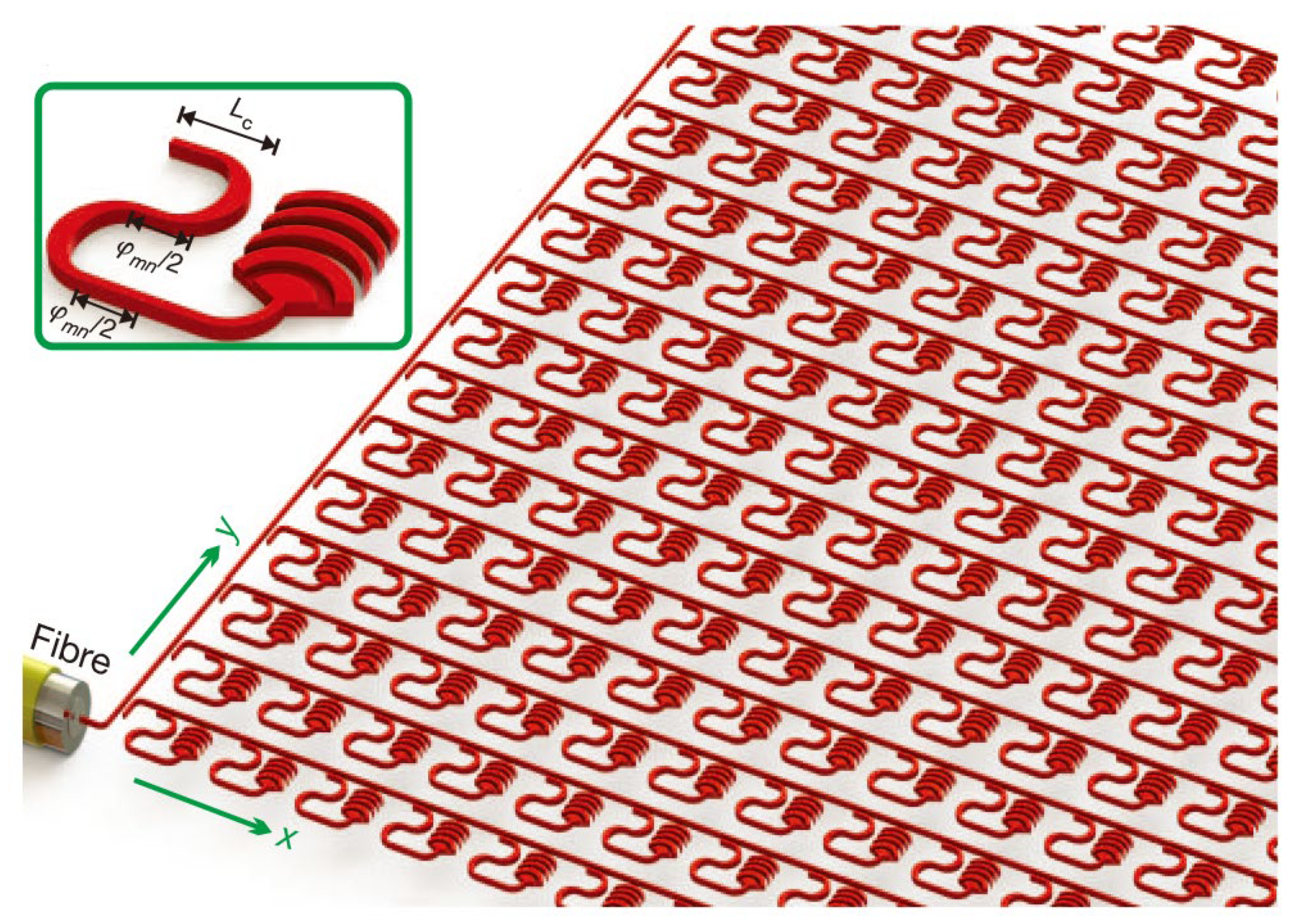
Figure 5. Schematic illustration of a 64 × 64 NPA system. The inset shows a diagram of a close-up view of one antenna unit cell. The length of directional coupler Lc can vary the coupling efficient and the two segments of the delay line can achieve a phase delay φmn [26].
In 2014, A. Yaacobi et al., from MIT reported a high-speed, low-power, and wide-scan-angle optical phased array [10]. This phased array is based on a novel phase-shifting architecture that utilizes 32-μm-long grating-based antennas, fed through evanescent field waveguide couplers from a bus waveguide in directly integrated thermo-optic phase shifters. The antenna gratings were designed using a shallow etch on the sides of the waveguide to ensure uniform emission from the decaying field. A laser with an eye-safe wavelength of 1550 nm was used for demonstration. Under the conditions of 10.6 V voltage and 18 mW average power, a continuous steering range of 51° was achieved. In addition, the device can also adapt to the wavelength range of 1.2 to 3.5 μm.
In 2016, C.V. Poulton et al., from MIT produced a phased array composed of 50 grating-based antennas [11]. The device achieves a 2D beam steering range of 46° × 36° by thermal and wavelength tuning, and the minimum beam spot is 0.85° × 0.18°. A schematic diagram of the device is shown in Figure 6. The phase shifters are cascaded into three groups. This design allows phase fine-tuning to compensate for noise caused by manufacturing errors. In addition, the cascade structure also allows three sets of phase shifters in the device to operate under different voltage conditions to generate three beams with different directions. In this research group, the antenna was etched on the edge of the waveguide using full etching, as shown in Figure 10b. This method can reduce the negative impact on the transmitting antenna caused by transition etching or insufficient etching of the waveguide.
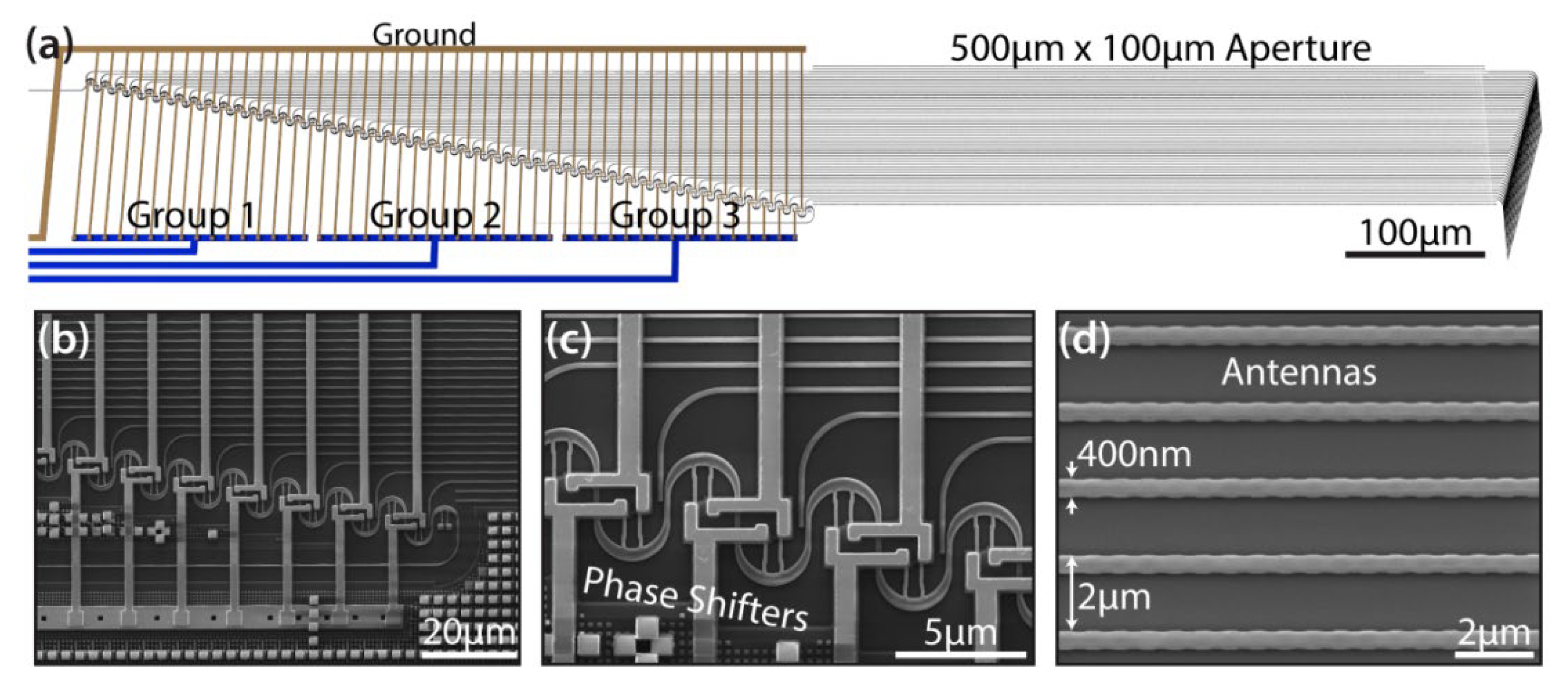
Figure 6. (a) SEM images of the (b) cascaded phase shifter architecture, (c) close-up of the thermal phase shifters, and (d) the full etch silicon grating-based antennas with a waveguide width of 400 nm and pitch of 2 µm [11].
In 2016, D.N. Hutchison et al. reported a large non-uniform emitter spacing optical phased array, fabricated in a 300 mm CMOS facility [12]. Due to the non-uniform arrangement of emitters, this array can suppress the side-lobe effect and improve the field of view. The device can achieve a beam steering Angle of 80° by thermo-optical phase modulation and a beam steering angle of 17° by wavelength tuning. This is equivalent to over 60,000 resolvable points in two-dimensional beam steering. In addition, a large number of phase-controlled emitters were used to control the average beam divergence at 0.14° (the minimum value was 0.11°).
In 2019, C.V. Poulton et al. reported a 512-path optical phased array [13]. They set up phase shifters for each path that can be controlled independently, which makes the transmitted wave front more flexible. The power consumption of the device is reduced to 1 mW. The longer antenna can increase the directivity of the emitter. A large scanning range of 56° × 15° can be achieved. The device uses a wideband photoelectric phase shifter for phase control. Compared with the traditional thermal optical phase shifter, this method not only reduces power consumption but also limits the crosstalk between adjacent elements. In addition, the OPA chip developed by this research group was applied to the Lidar for the first time, and the scanning experiment of 25 m was demonstrated. The real-time scanning image as shown in Figure 7 presents clear character contour features at 6 m.
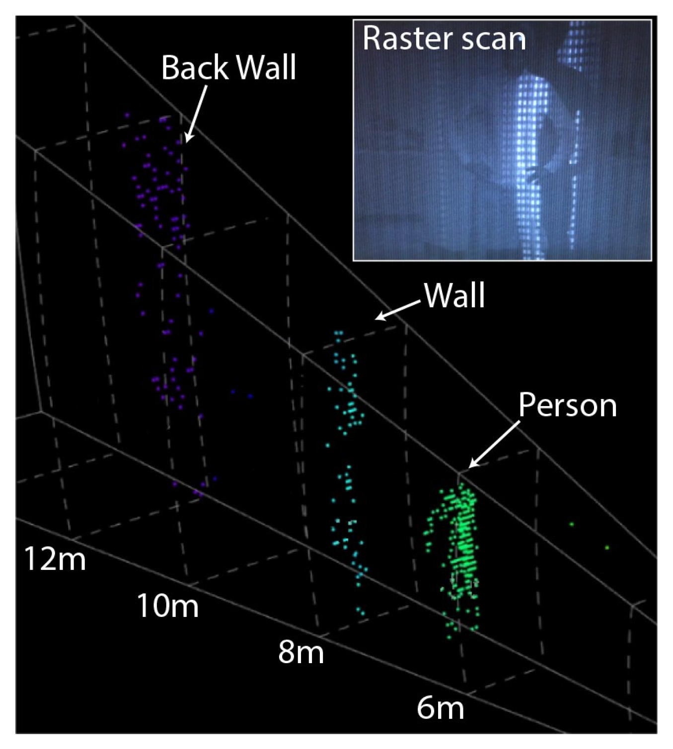
Figure 7. Real-time data from a 3D Lidar system consisting of raster scanning OPAs. Inset shows the scene being raster scanned [13].
In 2019, P. Bhargava et al. presented the first integrated coherent Lidar system with experimental ranging demonstrations operating within the eye-safe 1550 nm band [14]. Due to the tight pitch (2 μm) between antennas, the antennas can achieve high gain and strong rejection of interfering beams. Germanium is also used to construct a photoelectric detector with high response speed that can work within the safe range of human eyes. This device proves that high-performance solid-state Lidar can be realized at a low cost.
In 2020, S.A Miller, from Columbia University, reported a multi-pass 512-channel optical phased array [15], as shown in Figure 8a. The device adopts a multi-pass platform composed of a multi-mode waveguide embedded with a phase shifter, as shown in Figure 8b. This platform can cycle the light several times in the channel. During the cycle process, the beam will have orthogonal space conversion of different modes, so as to eliminate unnecessary interference and maintain broadband operation. The beam circulates in the channel and accumulates phase shifting, thus realizing the beam steering. In this way, the power consumption of large-scale optical phased arrays is reduced by nearly nine times while maintaining low loss across at least 100 nm of continuous optical bandwidth. It is demonstrated that the optical phased array can achieve 70° × 6° beam scanning under the condition of 1.9 W power consumption. The overall package is shown in Figure 8c. The size of the phased array chip is 8 mm × 15 mm.
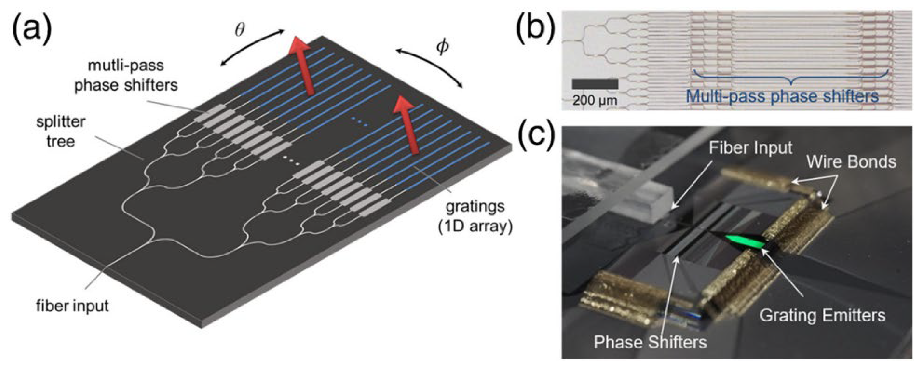
Figure 8. (a) Schematic (not to scale) of an optical phased array, showing out-of-plane beam emission (red arrows) and 2D steering. (b) Optical microscope image of the silicon waveguide layer of the fabricated chip. (c) Packaged device [15].
In 2022, S. Zhao et al. proposed a polarization multiplexing OPA with a bi-directional shared grating emitter array [16]. The system is composed of two phased arrays, a group of transmitting antenna arrays, multiple Mach-Zehnder interferometers (MZIs), and polarization factors (PSR). As shown in Figure 9, two identical OPAs are placed on either side of the transmitting antenna. MZIs and PSR are used to select the polarization state and propagation direction of the beam from the input to the transmitting antenna. The structure of the device improves the deflection range of the beam in the longitudinal direction. Through the test, this OPA can achieve longitudinal deflection of 54.5° by changing the wavelength from 1500 nm to 1600 nm when wavelength modulation efficiency is 0.545°/nm. Combined with phase modulation, the device can achieve a field of view angle of 54.5° × 77.8°. By increasing the number of antennas, the wavelength tuning range could be further improved. In addition, this OPA chip’s fabrication tolerance is high, reducing the fabrication difficulty.
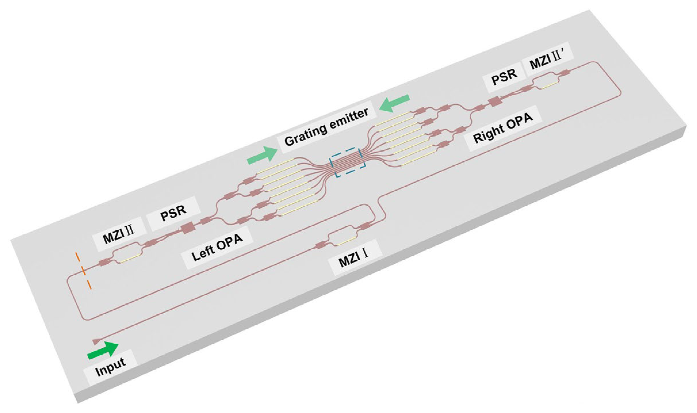
Figure 9. Schematic of the proposed bi-directional dual polarization multiplexed OPA. When the MZI I is on, the light injects into the grating emitter from the left side, otherwise from the right side [16].
3. OPA Lidar Based on Hybrid Material
In 2018, M. Zadka et al., from Columbia University, showed a hybrid silicon/silicon-nitride grating platform that overcomes the traditional trade-off between beam divergence and field of view [17]. Compared with Si-SiO2 waveguides, this platform is not sensitive to variations. Moreover, an 8 nm Al2O3 atomic layer is placed between the SiN and Si layers to serve as an etch-stop layer, thick enough to stop etching and thin enough to not disturb the entire device. The research group extended the length of a single antenna to 1 mm, increased the number of effective gratings, and made the beam divergence angle as low as 0.089°.
W. Xie, from the University of California, Santa Barbara, reported a high-density OPA system with heterogeneous phase shifters in 2019 [18]. The III-V PN diode is integrated into the silicon waveguides, and the diodes provide phase tuning for the optical mode in the hybrid III-V/Si waveguides. Combined with a star coupler and small spacing optical antenna, the phased array minimized the beam width at 0.02°, wavelength modulation efficiency reached 0.138°/nm, and a field of view of 51° × 28° was achieved. In addition, the device’s phase-shifter power consumption is extremely low, with static power consumption of less than 3 nW, wide optical bandwidth of more than 200 nm, and high operating speeds of more than 1 GHz. The chip composed of an optical phased array and a transceiver can further reduce the cost of Lidar and promote the development process of fully integrated Lidar.
In 2020, P. Wang et al., from the Institute of Semiconductors of the Chinese Academy of Sciences, proposed a SiN-Si dual-layer OPA chip [19]. The SiN layer is located above the SOI substrate with a spacing of 150 nm. The silicon devices and the SiN devices are located on two layers and do not interfere with each other, as shown in Figure 10. The input coupler and cascade beam splitter at the front end of OPA is a SiN device. The phase modulator and optical antenna at the back end are silicon devices. The SiN-Si chip can reduce the optical loss caused by the nonlinear effect when the silicon-based OPA works with high input power. At the same time, the front-end SiN device can handle very large optical power and is suitable for long-range detection.
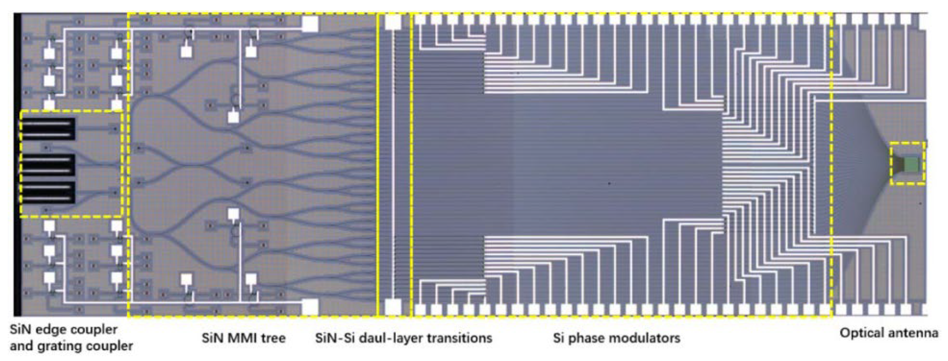
Figure 10. Optical micrograph of the proposed SiN-Si dual-layer optical phased array [19].
In 2021, C.S. Im et al. proposed an optical phased array with silicon nitride mixed polymer integration [20]. Unlike the traditional silicon nitride phased array, this polymer has a high thermal and optical effect. The device integrates the polymer phase modulator with the silicon nitride power distributor and antenna to solve the problem of low phased array modulation efficiency of silicon nitride materials. In addition, a steering angle magnifying lens is used to improve the modulation efficiency of the antenna. The test results show that the modulation power of each channel of the optical phased array is Pπ = 2.5 mW, and the field of view angle of 12° × 30° can be achieved. Finally, the research group combined this OPA to further produce the 3D Lidar based on ToF, and realize the scene scanning within 10 m. As shown in Figure 11, it is evidently found that a person at a distance of 8 m is distinguished from a wall at a distance of 10 m.
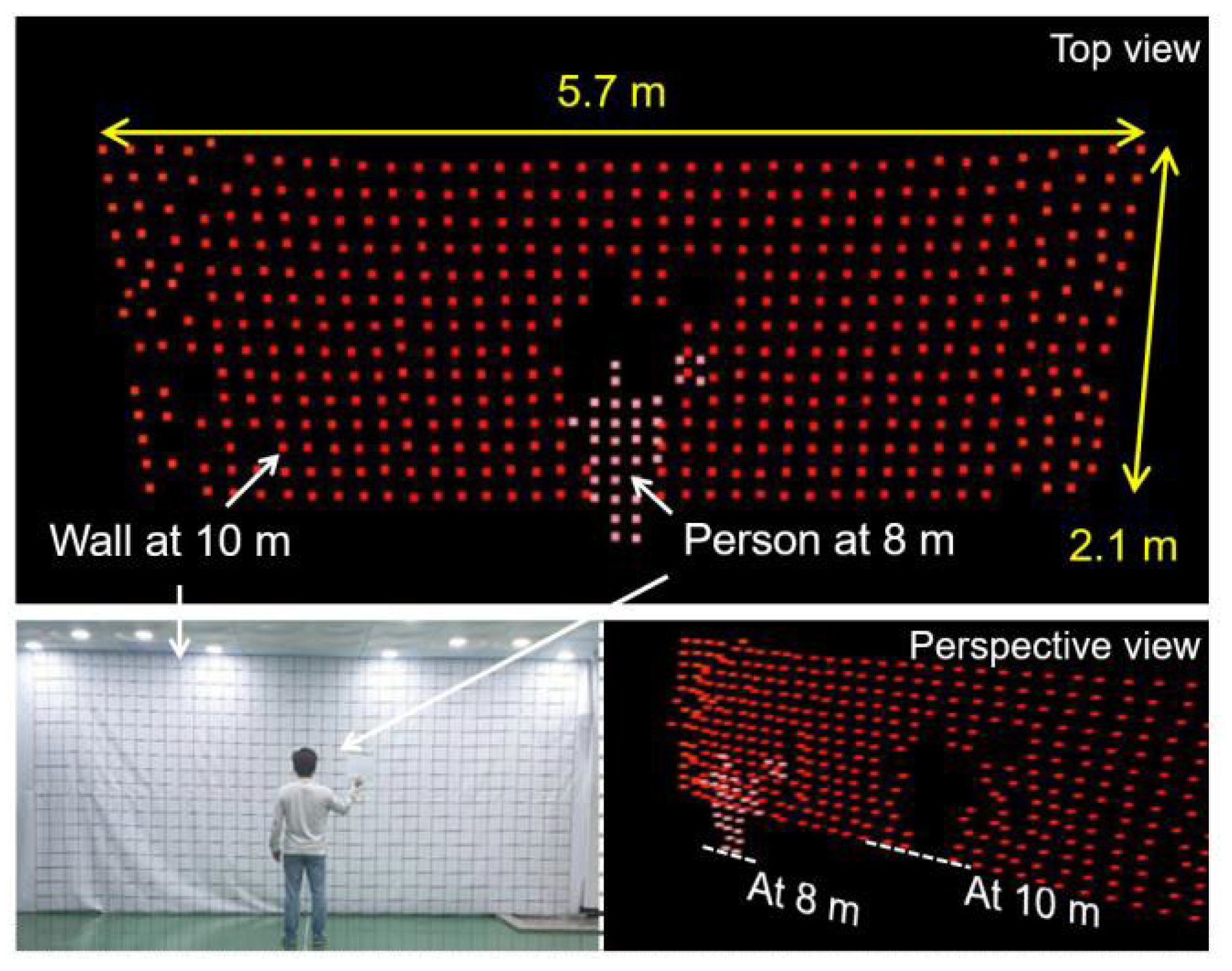
Figure 11. 3D raster-scanned image detected by the Lidar system based on the ToF scheme [20].
In the same year, L. Zhang et al. reported a multi-layer two-dimensional long-distance scanning optical phased array combining SiN and Si [21]. This device consists of a SiN base coupler, a SiN base beam splitter, and a Si base phase shifter. The beam is first coupled into the 200-um adiabatic waveguide by the mode-spot converter, then it is divided into 64 channels by the 6-stage Y beam splitter. Finally, the beam is transferred into the Si waveguide through the conical coupler. The device combines the advantages of the high-power processing capacity of SiN waveguides and the high thermal and optical modulation efficiency of the Si waveguide to show excellent performance. This OPA can realize the deflection angle of 96° × 14.4°. In addition, the OPA chip is used to successfully achieve long-range detection with up to 20 m distance in the ToF system and another test with a range of up to 109 m in the FMCW system.
From the above research progress of OPA Lidar, it can be found that researchers in various countries are striving to study the direction of miniaturization, low power consumption, and large field of view of Lidar. Despite the rapid development of OPA Lidar, some problems still need to be solved.
The problem of the side lobe is unavoidable for the on-chip Lidar made by the Fraunhofer diffraction effect, that is when the spacing of each incident waveguide is the same and larger than half wavelength, the side lobe that affects the scanning quality will appear. There are many methods to suppress the side lobe, among which the use of a non-equidistant waveguide phased array is relatively common. In 2016, Komljenovc et al. studied the non-equidistant waveguide phased array and proposed that the tiling method could realize the large-scale phased array with side-lobe suppression. In this research, some researchers have also designed side lobe suppression schemes, such as Xiao, using non-uniformly distributed optical waveguide devices to suppress side lobe generation, and Hutchison, using a phased array composed of a star coupler to effectively suppress the side lobe when the distance between waveguides is greater than half wavelength.
The scanning angle is still limited. Among all the OPA Lidar mentioned above, the maximum scanning field of view that can be achieved is 77.4° × 28.2°. Achieving a larger scanning field of view means increasing the difficulty of the production process and increasing the device cost. The simplest way to increase the scanning angle is to use a lens, which prevents the overall device from miniaturizing and reduces its stability. In addition, improving the efficiency of thermo-optical modulation can also achieve a larger scanning angle. For example, the double spiral structure waveguide proposed by Adam Densmore above reduces the volume and improves the efficiency of thermo-optical modulation.
References
- Hsu, C.P.; Li, B.; Solano-Rivas, B.; Gohil, A.R.; Chan, P.H.; Moore, A.D.; Donzella, V. A Review and Perspective on Optical Phased Array for Automotive Lidar. IEEE J. Sel. Top. Quantum Electron. 2020, 27, 8300416.
- Heck, M.J. Highly Integrated Optical Phased Arrays: Photonic Integrated Circuits for Optical Beam Shaping and Beam Steering. Nanophotonics 2017, 6, 93–107.
- Xiao, F.; Li, G.; Li, Y.; Xu, A. Fabrication of Irregular Optical Phased Arrays on Silicon-on-Insulator Wafers. Opt. Eng. 2008, 47, 040503.
- Van Acoleyen, K.; Bogaerts, W.; Jágerská, J.; Le Thomas, N.; Houdré, R.; Baets, R. Off-Chip Beam Steering with a One-Dimensional Optical Phased Array on Silicon-on-Insulator. Opt. Lett. 2009, 34, 1477–1479.
- Van Acoleyen, K.; Rogier, H.; Baets, R. Two-Dimensional Optical Phased Array Antenna on Silicon-on-Insulator. Opt. Express 2010, 18, 13655–13660.
- Doylend, J.K.; Heck, M.J.R.; Bovington, J.T.; Peters, J.D.; Coldren, L.A.; Bowers, J.E. Two-Dimensional Free-Space Beam Steering with an Optical Phased Array on Silicon-on-Insulator. Opt. Express 2011, 19, 21595–21604.
- Kwong, D.; Hosseini, A.; Zhang, Y.; Chen, R.T. 1 × 12 Unequally Spaced Waveguide Array for Actively Tuned Optical Phased Array on a Silicon Nanomembrane. Appl. Phys. Lett. 2011, 99, 051104.
- Van Acoleyen, K.; Komorowska, K.; Bogaerts, W.; Baets, R. One-Dimensional Off-Chip Beam Steering and Shaping Using Optical Phased Arrays on Silicon-on-Insulator. J. Light. Technol. 2011, 29, 3500–3505.
- Van Acoleyen, K.; Bogaerts, W.; Baets, R. Two-Dimensional Dispersive Off-Chip Beam Scanner Fabricated on Silicon-on-Insulator. IEEE Photonics Technol. Lett. 2011, 23, 1270–1272.
- Yaacobi, A.; Sun, J.; Moresco, M.; Leake, G.; Coolbaugh, D.; Watts, M.R. Integrated Phased Array for Wide-Angle Beam Steering. Opt. Lett. 2014, 39, 4575–4578.
- Poulton, C.V.; Yaacobi, A.; Su, Z.; Byrd, M.J.; Watts, M.R. Optical Phased Array with Small Spot Size, High Steering Range and Grouped Cascaded Phase Shifters. In Proceedings of the Integrated Photonics Research, Silicon and Nanophotonics, Vancouver, Canada, 18–20 July 2016; p. IW1B.2.
- Hutchison, D.N.; Sun, J.; Doylend, J.K.; Kumar, R.; Heck, J.; Kim, W.; Phare, C.T.; Feshali, A.; Rong, H. High-Resolution Aliasing-Free Optical Beam Steering. Optica 2016, 3, 887–890.
- Poulton, C.V.; Byrd, M.J.; Russo, P.; Timurdogan, E.; Khandaker, M.; Vermeulen, D.; Watts, M.R. Long-Range Lidar and Free-Space Data Communication with High-Performance Optical Phased Arrays. IEEE J. Sel. Top. Quantum Electron. 2019, 25, 7700108.
- Bhargava, P.; Kim, T.; Poulton, C.V.; Notaros, J.; Yaacobi, A.; Timurdogan, E.; Baiocco, C.; Fahrenkopf, N.; Kruger, S.; Ngai, T. Fully Integrated Coherent Lidar in 3d-Integrated Silicon Photonics/65nm Cmos. In Proceedings of the 2019 Symposium on VLSI Circuits, Kyoto, Japan, 9–14 June 2019; pp. C262–C263.
- Miller, S.A.; Chang, Y.C.; Phare, C.T.; Shin, M.C.; Zadka, M.; Roberts, S.P.; Stern, B.; Ji, X.; Mohanty, A.; Gordillo, O.A.J.; et al. Large-Scale Optical Phased Array Using a Low-Power Multi-Pass Silicon Photonic Platform. Optica 2020, 7, 3–6.
- Zhao, S.; Chen, J.; Shi, Y. Dual Polarization and Bi-Directional Silicon-Photonic Optical Phased Array with Large Scanning Range. IEEE Photonics J. 2022, 14, 6620905.
- Zadka, M.; Chang, Y.C.; Mohanty, A.; Phare, C.T.; Roberts, S.P.; Lipson, M. On-Chip Platform for a Phased Array with Minimal Beam Divergence and Wide Field-of-View. Opt. Express 2018, 26, 2528–2534.
- Xie, W.; Komljenovic, T.; Huang, J.; Tran, M.; Davenport, M.; Torres, A.; Pintus, P.; Bowers, J. Heterogeneous Silicon Photonics Sensing for Autonomous Cars. Opt. Express 2019, 27, 3642–3663.
- Wang, P.; Luo, G.; Xu, Y.; Li, Y.; Su, Y.; Ma, J.; Wang, R.; Yang, Z.; Zhou, X.; Zhang, Y.; et al. Design and Fabrication of a Sin-Si Dual-Layer Optical Phased Array Chip. Photonics Res. 2020, 8, 912–919.
- Im, C.S.; Kim, S.M.; Lee, K.P.; Ju, S.H.; Hong, J.H.; Yoon, S.W.; Kim, T.; Lee, E.S.; Bhandari, B.; Zhou, C.; et al. Hybrid Integrated Silicon Nitride–Polymer Optical Phased Array for Efficient Light Detection and Ranging. J. Light. Technol. 2021, 39, 4402–4409.
- Zhang, L.; Li, Y.; Chen, B.; Wang, Y.; Li, H.; Hou, Y.; Tao, M.; Li, Y.; Zhi, Z.; Liu, X.; et al. Two-Dimensional Multi-Layered Sin-on-Soi Optical Phased Array with Wide-Scanning and Long-Distance Ranging. Opt. Express 2022, 30, 5008–5018.
- Trinh, P.; Yegnanarayanan, S.; Coppinger, F.; Jalali, B. Silicon-on-Insulator (Soi) Phased-Array Wavelength Multi/Demultiplexer with Extremely Low-Polarization Sensitivity. IEEE Photonics Technol. Lett. 1997, 9, 940–942.
- Xiao, F.; Hu, W.; Xu, A. Optical Phased-Array Beam Steering Controlled by Wavelength. Appl. Opt. 2005, 44, 5429–5433.
- Xiao, F.; Li, G.; Xu, A. Cascade Arrangement of Irregular Optical Phased Arrays. Opt. Commun. 2008, 281, 1945–1949.
- Roelkens, G.; Van Thourhout, D.; Baets, R. High Efficiency Silicon-on-Insulator Grating Coupler Based on a Poly-Silicon Overlay. Opt. Express 2006, 14, 11622–11630.
- Sun, J.; Timurdogan, E.; Yaacobi, A.; Hosseini, E.S.; Watts, M.R. Large-Scale Nanophotonic Phased Array. Nature 2013, 493, 195–199.
More
Information
Subjects:
Instruments & Instrumentation
Contributors
MDPI registered users' name will be linked to their SciProfiles pages. To register with us, please refer to https://encyclopedia.pub/register
:
View Times:
4.0K
Revisions:
2 times
(View History)
Update Date:
07 Jul 2023
Table of Contents


Notice
You are not a member of the advisory board for this topic. If you want to update advisory board member profile, please contact office@encyclopedia.pub.
OK
Confirm
Only members of the Encyclopedia advisory board for this topic are allowed to note entries. Would you like to become an advisory board member of the Encyclopedia?
Yes
No
${ textCharacter }/${ maxCharacter }
Submit
Cancel
Back
Comments
${ item }
|
${ item.createdUser.fullName }
${ item.createdAt }
${ item.vote }
${ item.reply }
Delete
${ reply.createdUser.fullName }
${ reply.createdAt }
${ reply.vote }
Delete
There is no reply to this comment~
${ item.replyTextCharacter }/${ item.replyMaxCharacter }
Submit
Cancel
More
No more~
There is no comment~
${ textCharacter }/${ maxCharacter }
Submit
Cancel
${ selectedItem.replyTextCharacter }/${ selectedItem.replyMaxCharacter }
Submit
Cancel
Confirm
Are you sure to Delete?
Yes
No