Your browser does not fully support modern features. Please upgrade for a smoother experience.
Submitted Successfully!
 +1 credit
Thank you for your contribution! You can also upload a video entry or images related to this topic.
For video creation, please contact our Academic Video Service.
| Version | Summary | Created by | Modification | Content Size | Created at | Operation |
|---|---|---|---|---|---|---|
| 1 | Steponas Asmontas | -- | 2531 | 2023-06-30 15:33:22 | | | |
| 2 | Jessie Wu | Meta information modification | 2531 | 2023-07-03 04:31:33 | | |
Video Upload Options
We provide professional Academic Video Service to translate complex research into visually appealing presentations. Would you like to try it?
Cite
If you have any further questions, please contact Encyclopedia Editorial Office.
Ašmontas, S.; Mujahid, M. Halide Perovskite Materials for Solar Cells. Encyclopedia. Available online: https://encyclopedia.pub/entry/46279 (accessed on 25 July 2026).
Ašmontas S, Mujahid M. Halide Perovskite Materials for Solar Cells. Encyclopedia. Available at: https://encyclopedia.pub/entry/46279. Accessed July 25, 2026.
Ašmontas, Steponas, Muhammad Mujahid. "Halide Perovskite Materials for Solar Cells" Encyclopedia, https://encyclopedia.pub/entry/46279 (accessed July 25, 2026).
Ašmontas, S., & Mujahid, M. (2023, June 30). Halide Perovskite Materials for Solar Cells. In Encyclopedia. https://encyclopedia.pub/entry/46279
Ašmontas, Steponas and Muhammad Mujahid. "Halide Perovskite Materials for Solar Cells." Encyclopedia. Web. 30 June, 2023.
Copy Citation
The nomenclature “perovskite” was assigned to this structure in honor of Lev Perovski, the Russian mineralogist who initially unveiled it; since then, the name “perovskites” has been used to describe all materials that share calcium titanate’s crystal structure. The general formula for the perovskite light absorption layer is ABX3, where A is an organic cation (CH3NH3+), B is a metal cation (Pb2+), and X is a halide anion (I−).
cell
crystal
solar
fabrication
perovskite
tandem
materials
Physics
photo-voltaic
wide band
1. Halide Perovskite Materials for Solar Cells
Inorganic–organic halide solar cell researchers have become very interested in PSCs due to a striking rise in device efficiency from 3.8% [1] to 25.7% [2] since 2009. Considering an all-time high efficiency of around 26.7%, silicon PV systems hold most of the market share; perovskite has attracted much interest [3]. Given that certain materials have the potential to be employed in both photovoltaic PSCs and organic solar cells, this slight efficiency difference has recently caught the attention of researchers, particularly those with expertise in dye-sensitized solar cells (DSSCs) or organic solar cells. The DSSC device architecture is where PSCs display advantages over silicon-based devices, as seen in [4], which require labor-intensive and expensive high-vacuum deposition procedures. Based on the accounts of efficacious cell production on flexible substrates, further promise exists that the extensive roll-to-roll fabrication of PSCs could be implemented in various industrial sectors [5][6]. In 1839, German mineralogist Gustav Rose discovered a calcium titanate crystal structure. The nomenclature “perovskite” was assigned to this structure in honor of Lev Perovski, the Russian mineralogist who initially unveiled it; since then, the name “perovskites” has been used to describe all materials that share calcium titanate’s crystal structure. The general formula for the perovskite light absorption layer is ABX3, where A is an organic cation (CH3NH3+), B is a metal cation (Pb2+), and X is a halide anion (I−).
2. Crystal Structure
In Figure 1a–c, researchers can observe that the molecular structure of the organic halide perovskite is of the ABX3 type, where A and B are cations (with A being bigger than B), and X is the anion. The A cation (methylammonium, CH3NH3+, MA+, or formamidinium, CH3 (NH2)2+, FA+) in a perovskite’s unit cell is surrounded by 12 X anions (Cl−, Br−, or I−, or a coexistence of multiple halogens) to form a cuboctahedron. The octahedral position of X is occupied by the B cation (Pb2+, Sn2+, etc.) The octahedra of the B cation and X anion are connected to create a stable three-dimensional network structure[7][8][9]. For CH3NH3PbX3, as the size of the halide grows from X = Cl to Br, the unit cell parameter grows from 5.68 to 5.92 and then to 6.27 Å. Mixing halides makes it easy to adjust the cubic phase’s lattice characteristics; for example, CH3NH3PbBr2.3l0.7, CH3NH3PbBr2.07I0.93, and CH3NH3PbBr0.45I2.55 all displayed a = 5.98 Å, 6.03 Å, and 6.25 Å, respectively. The cubic perovskite structure of CH3NH3SnBrxl3−x (x = 0–3) crystallized unit cell parameters are reported as follows: a = 5.89 Å (x = 3), a = 6.01 Å (x = 2), and a = 6.24 Å (x = 0). Some Sn-based perovskite compounds showed conducting capabilities in contrast to Pb-based perovskite materials [10][11].
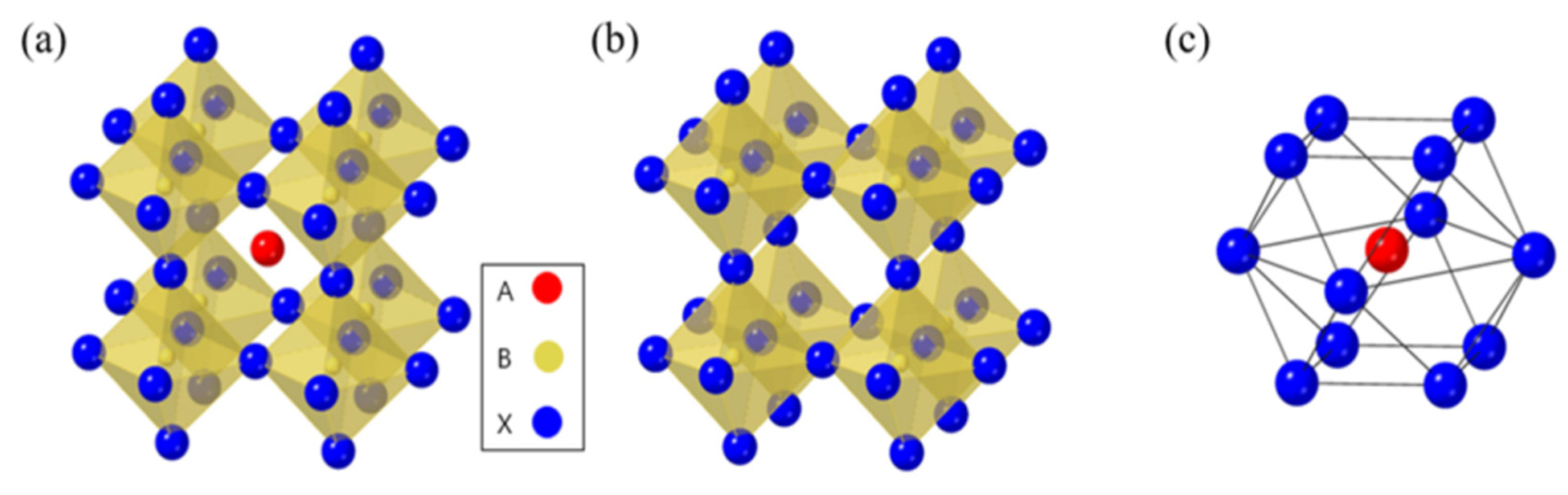
Figure 1. (a) The standard crystal structure of perovskite. (b) B cation and X anion crystal structure. (c) The A cation occupies the octahedron location of the X anion in the crystal structure [9]. Copyright 2019, MDPI.
A dimensionless value termed the Goldschmidt tolerance factor (t), which measures the crystal’s stability and its structure’s deformability, is used to predict the formability of different kinds of perovskites.
where the radius of cation A is rA, the radius of cation B is rB, and the radius of anion X is rX. For perovskite composed of a transition metal cation and an oxide anion, t = 1 is projected to result in a cubic structure, while t < 1 is predicted to result in octahedral deformation. Additionally, at t < 1, symmetry is lost, which impacts the electrical characteristics. Perovskite formability for alkali metal halides is anticipated to be 0.813 < t < 1.107 [12][13]. Cubic structures have tolerance factors between 0.89 and 1, with values greater than 0.89; due to the instability of B–X bonding in 3D, a transition to a 2D layer structure may occur. In contrast, a tetragonal (β phase) or orthorhombic (γ phase) structure may form if the tolerance factor is less than 0.89 [14]. The octahedral factor (µ), provided by Equation (2), is another component for perovskite formation.
Perovskite stability and distortion can be assessed through its utilization. The perovskite can have an octahedral factor between 0.45 and 0.89 without losing stability. Methylammonium lead trihalide (MAPbI3, where X is the halide, could be Cl, Br, or I) is PSC's most widely utilized absorber substance. As the size of the halide atom grows from Cl to Br to I, the unit cell characteristics rise from 5.68 to 5.92 to 6.27 Å. However, the increased size and aspherical shape of methylammonium (MA) cause the network to distort, which causes a phase change and a drop in temperature. The orthorhombic structure is present for T < 160 K, the tetragonal structure for T > 162.2 K to T < 327.4 K, and the cubic structure for T > 327.4 K. The bandgap of methylammonium lead halide typically ranges from 1.5 to 2.3 eV; MAPbI3 has a direct bandgap of roughly 1.55 eV, whereas MAPbBr3 has a relative WB of 2.3 eV for 600 nm absorption started. FAPbI3 (where FA is formamidinium) exhibits a NB of 1.48 eV as the absorber layer, indicating greater current extraction. However, this material has demonstrated lesser stability. The type of halogen atom employed also affects the structural characteristics of methylammonium lead halide. Lead halide perovskites have an octahedral crystal structure. The B cation (typically Pb but sometimes Sn) is octahedrally coupled to six halide ions. There is a shared corner between these octahedra, and the A cation lies between them [15][16]. The A cation of lead halide perovskites is either an organic molecule (methylammonium, MA, CH3NH3+) or an inorganic cation (usually Cs+), leading to the further categorization of lead halide perovskites as either organic–inorganic (hybrid) or all-inorganic. One can manipulate perovskites’ optical and electrical characteristics by changing the proportions of formed halide ions and, to a lesser extent, the cations [17]. Like traditional metal chalcogenide semiconductors, perovskites’ optical characteristics and object tuning can be achieved by adjusting their dimensions and size. Perovskites exhibit a pronounced inclination towards the creation of stratified two-dimensional (2D) and quasi-two-dimensional architectures, even though their dimensional range can be altered from three-dimensional to zero-dimensional by manipulating the synthetic parameters employed [18][18][19][19][20]. Numerous recent investigations have demonstrated the excellent photoluminescence quantum yields of colloidal perovskite nanocrystals. Furthermore, when their dimensional changes are reduced from 3D to 2D, they exhibit significant quantum confinement effects, allowing for the further customization of optical characteristics [21][22]. A good number of applications, such as solar cells and lasers, LEDs, and PV, have demonstrated the immense potential of perovskite.
3. Electronic Structure
Here, by considering the perovskite material’s electronic characteristics to understand its layered perovskite structure. Density functional theory (DFT) computer simulations were used in several theoretical investigations on the density of states (DOS) of perovskites, correlating the composition of the bands with the DOS. Researchers may learn more about where those remarkable optoelectronic capabilities of perovskite materials come from and how they can be optimized with the help of the DFT calculations performed on metal halide perovskites. The valence band results from the overlap between the M-site cation’s ns orbitals and the X-site anions’ np orbitals. In contrast, the conduction band is formed by combining the np orbitals of the M cation and the X anions [23][24]. It is well established that there is an antibonding feature between the valence band maximum (VBM) and the conduction band minimum (CBM) because of the orbital overlap among the filled ns of M and np of X [25][26]. The ionic nature of bonds expands, and Eg increases when the composition shifts from I to Cl because the energy difference between ns and np halogen atomic orbitals widens.
M metals have a less noticeable impact on the band structure. The final band structure is influenced by phenomena such as ns2 lone pairs, the relativistic stabilization of the 6s2 level in Pb2+, and the composition of M–X bonds (degree of covalence). Considering all these characteristics, the Eg of these materials can be precisely tuned by altering their compositions or making alloys. In addition, the absence of electron–phonon coupling in perovskites’ straight bandgap makes electronic transitions more likely. Since the electron’s quantized wave motion in a periodic crystalline lattice is connected to its crystal momentum (vector k), the VBM and CBM in direct bandgap materials are coplanar about this axis. Yin et al. computed the band structure and DOS of the cubic phase MAPbI3 using DFT–PBE computation. The band structures of the tetragonal and orthorhombic phases of MAPbI3 are very close to those of the cubic phase, according to a subsequent investigation by the same group. According to the experimental findings, the bandgaps are expected to be 1.55 and 1.57 eV in the tetragonal and cubic phases, respectively, and the UV-vis measurement of FASnI3 is illustrated in Figure 2 [27][28]. Since the VBM and CBM coincide at the same point of the Brillouin zone, cubic MAPbI3 is a direct bandgap semiconductor. The two MAPbI3 phases, tetragonal and orthorhombic, are direct bandgap semiconductors exhibiting values that are nearly close to one another. The comparison between the experimental UV-vis spectrum of MAPbI3 (red line) and the SOC–GW calculated spectrum (blue line) is depicted [27][29]. The Pb p orbital dominates the CBM, while I p states, through a minor addition from Pb s states, dominate the VBM. Given its position well below the VBM, the MA cation’s partial DOS does not make any direct electronic contributions to the CBM or VBM. MAPbI3’s remarkable electrical properties can be traced back to a lone pair of s orbital electrons in the Pb cation. While the outer s orbitals of most metal cations are empty, Pb possesses an occupied 6s orbital just under the valence band [23][30].
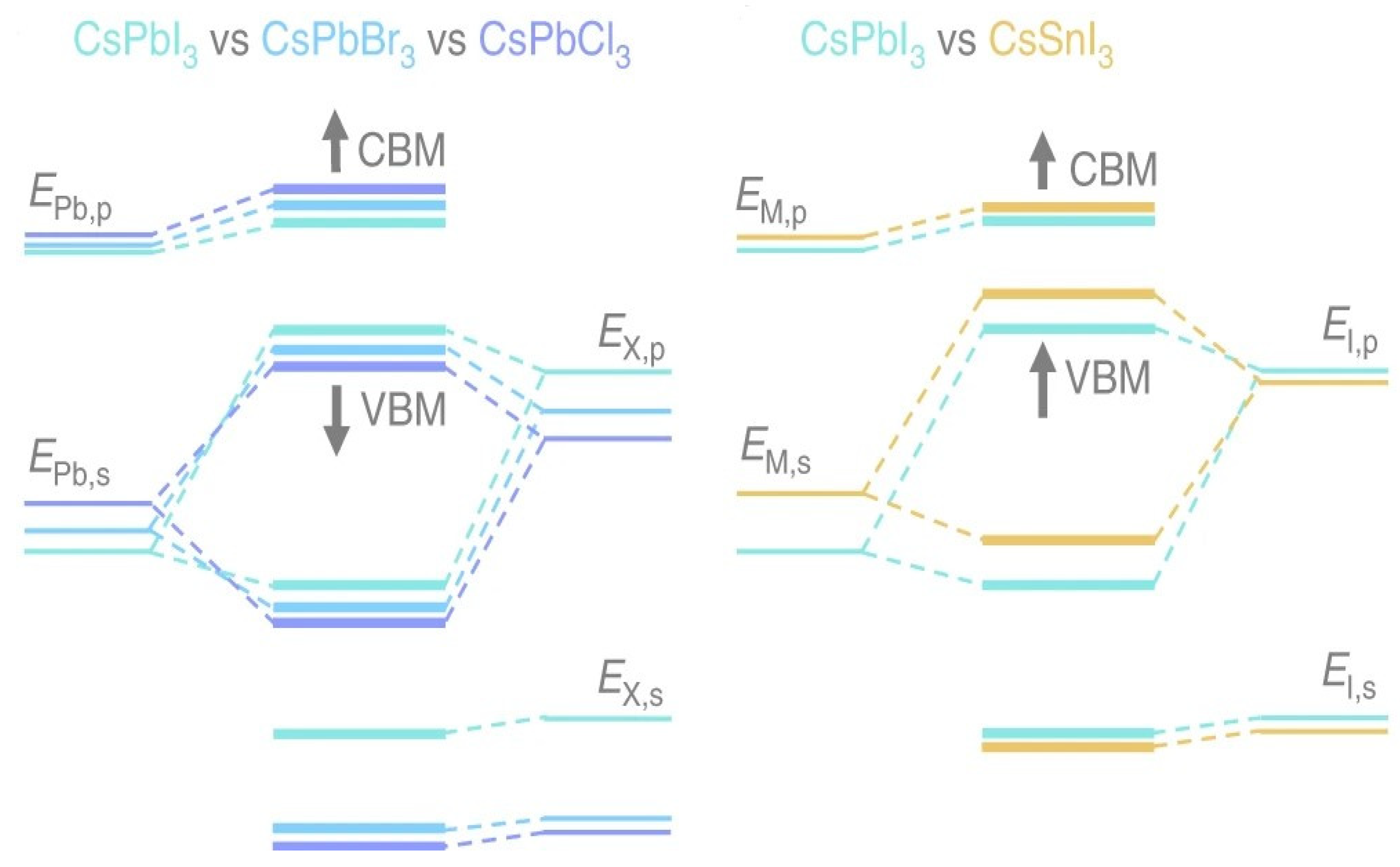
Figure 2. Different compositions of 3D halide perovskites have different energy levels [26]. Copyright 2019, Nature.
4. Structure of Perovskite Solar Cells
Efficient PSCs could be the most fantastic solution for commercial solar technology manufacturing. PSC products are likewise separated into two categories for a good reason: normal and inverted [31]. The hole transport layer (HTL) or the electron transport layer (ETL) should be placed first; there are two distinct methods for fabricating PSCs. Semiconducting p-type polymers create an inverted structure, such as PEDOT: PSS, while the standard structure uses n-type semiconductors, such as TiO2. The first ETL employing titanium oxide (TiO2) was built in 2009, and it was the predecessor of the current structure. A PIN-type product based on the organic HTL poly(3,4-ethylene dioxythiophene)-co-polystyrene sulfate (PEDOT: PSS) was released four years later. These two architectures currently have the highest PCEs reported [4][32][33][34][35]. By employing growth methods, the fabrication temperature for n–i–p structured flexible PSCs could be kept to a minimum. However, an n–i–p structure device requires an excessive temperature method to develop a compact TiO2 coating. Plastic is not a suitable surface for this [31]. The mesoporous TIO2 film was initially employed as a scaffold for the initial PSCs fabricated from dye-sensitive solar cells (DSCs); as a result of sintering nanoparticles (NP), a porous TiO2 layer developed, with the self-assembled perovskite absorber providing the filler.
It is easier to transfer electrons between the FTO electrode and the perovskite absorber, and a perovskite coating was formed on mesoporous TiO2 [36]. Perovskite NPs work to progressively strip the photoexcited pigment of its electrons, enabling it to serve mainly as a light absorber in place of the molecular sensitizer it formerly was. However, the finding that organic–inorganic halide perovskite could independently conduct electrons and holes encouraged the creation of future devices. The mesoscopic variant’s perovskite capping layer extends well beyond the nanostructure thanks to the semiconductor oxide scaffold’s thoroughly infiltrated pores. The planar structure was researched to facilitate fabrication. Planar metal oxide ETL fabrication typically occurs below 200 °C without impairing the perovskite devices’ functionality. The standard structure is thus receiving much attention for further research [37][38]. Such a lower temperatures solution technique might result in the fabrication of the ETL, so the p–i–n-type arrangement has gained even greater notoriety.
Along with the electron-transporting material (ETM) layer, a hole-transporting material (HTM) layer was also applied; perovskites were suited for hole transport. This has been a major component in manufacturing p–i–n-structured solar cells. HTLs are well-suited for adaptable perovskite optoelectrical devices since their production often does not need a high-temperature annealing procedure [39][40]. HTM is also an air- and water-resistant alternative for PSCs. To prevent leakage, the objective of producing planar p–i–n on a uniform transparent conductive oxides (TCO) electrode is to manufacture a perovskite layer without pinholes by utilizing a one-step spin-coating procedure. Results from cells produced from a 1:1 molar PbI2/CH3NH3I solution are inferior to those from the 1:3 molar PbCl2/CH3NH3I solutions. The annealed perovskite film still exhibited pores and poor crystallinity since no scaffold had been used at 100 °C [41][42]. These findings prove that the perovskite layer’s appearance and crystallinity are critical to the device’s performance.
Utilizing the advantages of perovskite materials—known for their direct bandgap, high absorption coefficient, and superior charge transport properties—researchers have been designing and optimizing tandem solar cells. These perovskite tandem solar cells typically consist of a perovskite top cell paired with a bottom cell, often composed of silicon or another perovskite variant. This configuration broadens the solar spectrum coverage, thereby amplifying overall efficiency. Moreover, advancements have been made in improving the stability of these cells, with notable progress in encapsulation techniques and tweaks to perovskite composition that significantly reduce degradation over time. Despite these strides, challenges persist in areas such as large-scale manufacturing, consistency in the fabrication of thin films, and long-term stability, among others. However, the potential of perovskite tandem solar cells continues to drive substantial research and commercial interest. The Cell designs, structure, and applications of perovskite materials in tandem devices are depicted in Figure 3.
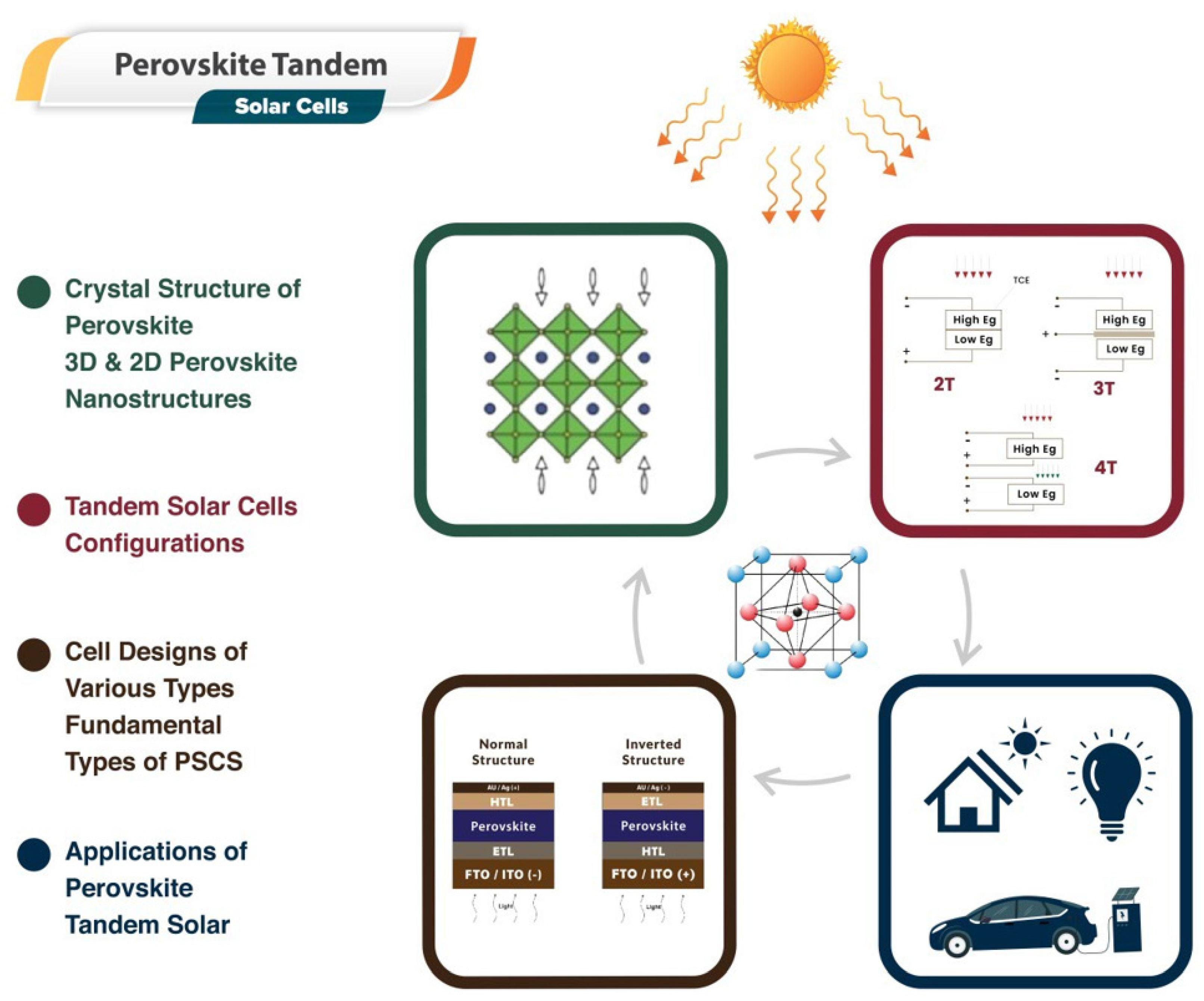
Figure 3. A sketch map of the solar cells fabrication for industrial application
Recent research has shown that greater PCEs can be obtained using organic–inorganic hybrid halide perovskite materials (CH3NH3PbI3) instead of Si single-junction cells with advanced PV technology. For this reason, hybrid metallic halide perovskite materials, which are both organic and inorganic, share the benefits of both types of compounds. Because their performances increase higher than silicon-based PV technology, the newly developed perovskite solar cell (PSC) has been recognized as something that might drastically change the PV market. PSCs have captured significant interest in the solar world due to their bandgap's higher efficiency, minimal cost, process compatibility, and adjustability. With their widely-accepted bandgap of 1.1 eV, high open-circuit voltage (VOC) of up to 750 mV, cheap manufacturing due to their supremacy in the industry, and exceptionally high efficiency, crystalline silicon solar cells are almost perfect for use in these tandem cells [43][44]. Nevertheless, the widespread use of III–V solar cells’ expensive manufacturing processes prevents them from being used for practical uses. The advancement of perovskite-based PV technology provided a viable solution to the need for inexpensive high-efficiency solar panels [45].
References
- Lin, Q.; Armin, A.; Nagiri, R.C.R.; Burn, P.L.; Meredith, P. Electro-optics of perovskite solar cells. Nat. Photonics 2015, 9, 106–112.
- Li, Y.; Meng, L.; Yang, Y.M.; Xu, G.; Hong, Z.; Chen, Q.; You, J.; Li, G.; Yang, Y.; Li, Y. High-efficiency robust perovskite solar cells on ultrathin flexible substrates. Nat. Commun. 2016, 7, 10214.
- Green, M.A.; Dunlop, E.D.; Hohl-Ebinger, J.; Yoshita, M.; Kopidakis, N.; Bothe, K.; Hinken, D.; Rauer, M.; Hao, X. Solar cell efficiency tables (Version 60). Photovoltaics 2022, 30, 687–701.
- Kojima, A.; Teshima, K.; Shirai, Y.; Miyasaka, T. Organometal halide perovskites as visible-light sensitizers for photovoltaic cells. J. Am. Chem. Soc. 2009, 131, 6050–6051.
- Kumar, M.H.; Yantara, N.; Dharani, S.; Graetzel, M.; Mhaisalkar, S.; Boix, P.P.; Mathews, N. Flexible, low-temperature, solution processed ZnO-based perovskite solid state solar cells. Chem. Commun. 2013, 49, 11089–11091.
- Shin, S.S.; Yang, W.S.; Noh, J.H.; Suk, J.H.; Jeon, N.J.; Park, J.H.; Kim, J.S.; Seong, W.M.; Seok, S.I. High-performance flexible perovskite solar cells exploiting Zn2SnO4 prepared in solution below 100 °C. Nat. Commun. 2015, 6, 7410.
- Pena, M.; Fierro, J.L. Chemical structures and performance of perovskite oxides. Chem. Rev. 2001, 101, 1981–2018.
- Zhang, F.; Zhong, H.; Chen, C.; Wu, X.-g.; Hu, X.; Huang, H.; Han, J.; Zou, B.; Dong, Y. Brightly luminescent and color-tunable colloidal CH3NH3PbX3 (X = Br, I, Cl) quantum dots: Potential alternatives for display technology. ACS Nano. 2015, 9, 4533–4542.
- Kim, D.; Lee, D.-K.; Kim, S.M.; Park, W.; Sim, U. Photoelectrochemical Water Splitting Reaction System Based on Metal-Organic Halide Perovskites. Materials. 2020, 13, 210.
- Mitzi, D.B.; Feild, C.; Harrison, W.; Guloy, A.J.N. Conducting tin halides with a layered organic-based perovskite structure. Nature 1994, 369, 467–469.
- Wang, H.; He, J.; Xiang, H.; Ran, R.; Zhou, W.; Wang, W.; Shao, Z.J.E. Additive Engineering for Mixed Lead–Tin Narrow-Band-Gap Perovskite Solar Cells: Recent Advances and Perspectives. Energy Fuels 2023, 37, 6401–6423.
- Rini, M.; Tobey, R.; Dean, N.; Itatani, J.; Tomioka, Y.; Tokura, Y.; Schoenlein, R.W.; Cavalleri, A. Control of the electronic phase of a manganite by mode-selective vibrational excitation. Nature 2007, 449, 72–74.
- Li, C.; Lu, X.L.; Ding, W.; Feng, L.; Gao, Y.; Guo, Z. Formability of ABX3 (X = F, Cl, Br, I) halide perovskites. Acta Cryst. 2008, 64, 702–707.
- Chilvery, A.; Das, S.; Guggilla, P.; Brantley, C.; Sunda-Meya, A.J.S. A perspective on the recent progress in solution-processed methods for highly efficient perovskite solar cells. Sci. Technol. Adv. Mater. 2016, 17, 650–658.
- Huang, H.; Polavarapu, L.; Sichert, J.A.; Susha, A.S.; Urban, A.S.; Rogach, A.L. Colloidal lead halide perovskite nanocrystals: Synthesis, optical properties and applications. NPG Asia Mater. 2016, 8, e328.
- Christians, J.A.; Miranda Herrera, P.A.; Kamat, P.V. Transformation of the Excited State and Photovoltaic Efficiency of CH3NH3PbI3 Perovskite upon Controlled Exposure to Humidified Air. J. Am. Chem. Soc. 2015, 137, 1530–1538.
- Eperon, G.E.; Stranks, S.D.; Menelaou, C.; Johnston, M.B.; Herz, L.M.; Snaith, H.J. Formamidinium lead trihalide: A broadly tunable perovskite for efficient planar heterojunction solar cells. Energy Environ. Sci. 2014, 7, 982–988.
- Sun, S.; Yuan, D.; Xu, Y.; Wang, A.; Deng, Z. Ligand-mediated synthesis of shape-controlled cesium lead halide perovskite nanocrystals via reprecipitation process at room temperature. ACS Nano 2016, 10, 3648–3657.
- Wu, X.; Trinh, M.T.; Niesner, D.; Zhu, H.; Norman, Z.; Owen, J.S.; Yaffe, O.; Kudisch, B.J.; Zhu, X.-Y. Trap states in lead iodide perovskites. J. Am. Chem. Soc. 2015, 137, 2089–2096.
- Sichert, J.A.; Tong, Y.; Mutz, N.; Vollmer, M.; Fischer, S.; Milowska, K.Z.; García Cortadella, R.; Nickel, B.; Cardenas-Daw, C.; Stolarczyk, J.K. Quantum size effect in organometal halide perovskite nanoplatelets. Nano Lett. 2015, 15, 6521–6527.
- Huang, H.; Susha, A.S.; Kershaw, S.V.; Hung, T.F.; Rogach, A.L. Control of emission color of high quantum yield CH3NH3PbBr3 perovskite quantum dots by precipitation temperature. Adv. Sci. 2015, 2, 1500194.
- Schmidt, L.C.; Pertegás, A.; González-Carrero, S.; Malinkiewicz, O.; Agouram, S.; Minguez Espallargas, G.; Bolink, H.J.; Galian, R.E.; Pérez-Prieto, J. Nontemplate synthesis of CH3NH3PbBr3 perovskite nanoparticles. J. Am. Chem. Soc. 2014, 136, 850–853.
- Yin, W.-J.; Yang, J.-H.; Kang, J.; Yan, Y.; Wei, S.-H. Halide perovskite materials for solar cells: A theoretical review. J. Mater. Chem. A 2015, 3, 8926–8942.
- Even, J.; Pedesseau, L.; Jancu, J.-M.; Katan, C. Importance of spin–orbit coupling in hybrid organic/inorganic perovskites for photovoltaic applications. J. Phys. Chem. Lett. 2013, 4, 2999–3005.
- Walsh, A.; Watson, G.W. The origin of the stereochemically active Pb (II) lone pair: DFT calculations on PbO and PbS. J. Solid State Chem. 2005, 178, 1422–1428.
- Tao, S.; Schmidt, I.; Brocks, G.; Jiang, J.; Tranca, I.; Meerholz, K.; Olthof, S. Absolute energy level positions in tin- and lead-based halide perovskites. Nat. Commun. 2019, 10, 2560.
- Yin, W.-J.; Shi, T.; Yan, Y. Unusual defect physics in CH3NH3PbI3 perovskite solar cell absorber. Appl. Phys. Lett. 2014, 104, 063903.
- Yin, W.J.; Shi, T.; Yan, Y. Unique properties of halide perovskites as possible origins of the superior solar cell performance. Adv. Mater. 2014, 26, 4653–4658.
- Umari, P.; Mosconi, E.; De Angelis, F. Relativistic GW calculations on CH3NH3PbI3 and CH3NH3SnI3 perovskites for solar cell applications. Sci. Rep. 2014, 4, 4467.
- Walsh, A.; Payne, D.J.; Egdell, R.G.; Watson, G.W. Stereochemistry of post-transition metal oxides: Revision of the classical lone pair model. Chem. Soc. Rev. 2011, 40, 4455–4463.
- Mujahid, M.; Chen, C.; Hu, W.; Wang, Z.-K.; Duan, Y. Progress of High-Throughput and Low-Cost Flexible Perovskite Solar Cells. Sol. RRL 2020, 4, 1900556.
- Jeng, J.Y.; Chiang, Y.F.; Lee, M.H.; Peng, S.R.; Guo, T.F.; Chen, P.; Wen, T.C. CH3NH3PbI3 perovskite/fullerene planar-heterojunction hybrid solar cells. Adv. Mater. 2013, 25, 3727–3732.
- Yang, W.S.; Park, B.-W.; Jung, E.H.; Jeon, N.J.; Kim, Y.C.; Lee, D.U.; Shin, S.S.; Seo, J.; Kim, E.K.; Noh, J.H. Iodide management in formamidinium-lead-halide–based perovskite layers for efficient solar cells. Science 2017, 356, 1376–1379.
- Green, M.A.; Dunlop, E.D.; Hohl-Ebinger, J.; Yoshita, M.; Kopidakis, N.; Ho-Baillie, A.W. Solar cell efficiency tables (Version 55). Prog. Photovolt. 2019, 1, 3–15.
- Chen, B.; Bai, Y.; Yu, Z.; Li, T.; Zheng, X.; Dong, Q.; Shen, L.; Boccard, M.; Gruverman, A.; Holman, Z. Efficient semitransparent perovskite solar cells for 23.0%-efficiency perovskite/silicon four-terminal tandem cells. Adv. Energy Mater. 2016, 6, 1601128.
- Grätzel, C.; Zakeeruddin, S.M. Recent trends in mesoscopic solar cells based on molecular and nanopigment light harvesters. Mater. Today 2013, 16, 11–18.
- Grätzel, M. The light and shade of perovskite solar cells. Nat. Mater. 2014, 13, 838–842.
- Chen, W.; Wu, Y.; Yue, Y.; Liu, J.; Zhang, W.; Yang, X.; Chen, H.; Bi, E.; Ashraful, I.; Grätzel, M. Efficient and stable large-area perovskite solar cells with inorganic charge extraction layers. Science 2015, 350, 944–948.
- Yang, D.; Yang, R.; Zhang, J.; Yang, Z.; Liu, S.F.; Li, C. High efficiency flexible perovskite solar cells using superior low temperature TiO2. Energy Environ. Sci. 2015, 8, 3208–3214.
- Kim, H.-S.; Lee, C.-R.; Im, J.-H.; Lee, K.-B.; Moehl, T.; Marchioro, A.; Moon, S.-J.; Humphry-Baker, R.; Yum, J.-H.; Moser, J.E. Lead iodide perovskite sensitized all-solid-state submicron thin film mesoscopic solar cell with efficiency exceeding 9%. Sci. Rep. 2012, 2, 591.
- You, J.; Hong, Z.; Yang, Y.; Chen, Q.; Cai, M.; Song, T.-B.; Chen, C.-C.; Lu, S.; Liu, Y.; Zhou, H. Low-temperature solution-processed perovskite solar cells with high efficiency and flexibility. ACS Nano 2014, 8, 1674–1680.
- Wang, Q.; Shao, Y.; Dong, Q.; Xiao, Z.; Yuan, Y.; Huang, J. Large fill-factor bilayer iodine perovskite solar cells fabricated by a low-temperature solution-process. Energy Environ. Sci. 2014, 7, 2359–2365.
- Yoshikawa, K.; Kawasaki, H.; Yoshida, W.; Irie, T.; Konishi, K.; Nakano, K.; Uto, T.; Adachi, D.; Kanematsu, M.; Uzu, H. Silicon heterojunction solar cell with interdigitated back contacts for a photoconversion efficiency over 26%. Nat. Energy 2017, 2, 17032.
- Taguchi, M.; Yano, A.; Tohoda, S.; Matsuyama, K.; Nakamura, Y.; Nishiwaki, T.; Fujita, K.; Maruyama, E. 24.7% record efficiency HIT solar cell on thin silicon wafer. IEEE J. Photovolt. 2013, 4, 96–99.
- Correa-Baena, J.-P.; Abate, A.; Saliba, M.; Tress, W.; Jacobsson, T.J.; Grätzel, M.; Hagfeldt, A.J.E.; Science, E. The rapid evolution of highly efficient perovskite solar cells. Energy Environ. Sci. 2017, 10, 710–727.
More
Information
Subjects:
Engineering, Electrical & Electronic
Contributors
MDPI registered users' name will be linked to their SciProfiles pages. To register with us, please refer to https://encyclopedia.pub/register
:
View Times:
896
Revisions:
2 times
(View History)
Update Date:
03 Jul 2023
Table of Contents


Notice
You are not a member of the advisory board for this topic. If you want to update advisory board member profile, please contact office@encyclopedia.pub.
OK
Confirm
Only members of the Encyclopedia advisory board for this topic are allowed to note entries. Would you like to become an advisory board member of the Encyclopedia?
Yes
No
${ textCharacter }/${ maxCharacter }
Submit
Cancel
Back
Comments
${ item }
|
${ item.createdUser.fullName }
${ item.createdAt }
${ item.vote }
${ item.reply }
Delete
${ reply.createdUser.fullName }
${ reply.createdAt }
${ reply.vote }
Delete
There is no reply to this comment~
${ item.replyTextCharacter }/${ item.replyMaxCharacter }
Submit
Cancel
More
No more~
There is no comment~
${ textCharacter }/${ maxCharacter }
Submit
Cancel
${ selectedItem.replyTextCharacter }/${ selectedItem.replyMaxCharacter }
Submit
Cancel
Confirm
Are you sure to Delete?
Yes
No