Your browser does not fully support modern features. Please upgrade for a smoother experience.
Submitted Successfully!
 +1 credit
Thank you for your contribution! You can also upload a video entry or images related to this topic.
For video creation, please contact our Academic Video Service.
| Version | Summary | Created by | Modification | Content Size | Created at | Operation |
|---|---|---|---|---|---|---|
| 1 | Lirong Zhao | -- | 1997 | 2023-06-20 10:58:45 | | | |
| 2 | Catherine Yang | Meta information modification | 1997 | 2023-06-21 03:46:35 | | |
Video Upload Options
We provide professional Academic Video Service to translate complex research into visually appealing presentations. Would you like to try it?
Cite
If you have any further questions, please contact Encyclopedia Editorial Office.
Zhao, L.; Cui, Y.; Li, J.; Xie, Y.; Li, W.; Zhang, J. Focused Ion Beam technology. Encyclopedia. Available online: https://encyclopedia.pub/entry/45846 (accessed on 25 July 2026).
Zhao L, Cui Y, Li J, Xie Y, Li W, Zhang J. Focused Ion Beam technology. Encyclopedia. Available at: https://encyclopedia.pub/entry/45846. Accessed July 25, 2026.
Zhao, Lirong, Yimin Cui, Junyi Li, Yuxi Xie, Wenping Li, Junying Zhang. "Focused Ion Beam technology" Encyclopedia, https://encyclopedia.pub/entry/45846 (accessed July 25, 2026).
Zhao, L., Cui, Y., Li, J., Xie, Y., Li, W., & Zhang, J. (2023, June 20). Focused Ion Beam technology. In Encyclopedia. https://encyclopedia.pub/entry/45846
Zhao, Lirong, et al. "Focused Ion Beam technology." Encyclopedia. Web. 20 June, 2023.
Copy Citation
Nanomaterials with unique structures and functions have been widely used in the fields of microelectronics, biology, medicine, and aerospace, etc. With advantages of high resolution and multi functions (e.g., milling, deposition, and implantation), focused ion beam (FIB) technology has been widely developed due to urgent demands for the 3D fabrication of nanomaterials.
3D controllable fabrication
FIB-SEM synchronization system
ion–sample interaction
1. FIB Optical System
1.1. Ion Sources
As the origin of the ion beam, the performances of ion sources determine the current and spot of FIB at a sample directly. There are many parameters for characterizing this ion source, such as the emission type, brightness βr, energy spread ΔEFWHMΔEFWHM, source spot, and stability. Table 1 shows the performances of the current commercial ion sources. Among them, the LMIS gallium ion source is mostly used due to its low melting point (~30 °C), low volatility, low vapor pressure, high emission, and low surface free energy [1]. Compared with other ion sources, the Ga+ source has a relatively simple structure, as shown in Figure 1a. The tip is also called a Taylor tip, which is formed via ion emission from a liquid metal under the strong electric field. The Ga+ source can meet the requirements of submicron fabrication, as its source spot is about 50–100 nm, its brightness can reach 106 Am−2sr−1V−1106 Am−2sr−1V−1, and its emission is very stable. Generally, it can work at 3000 µA·h.

Figure 1. (a–d) Schematic diagrams of liquid metal ion source (LMIS) Ga, gas field ionization source (GFIS) He, inductively coupled plasma (ICP) source Xe, and electron cyclotron resonance (ECR) plasma ion source, respectively.
Table 1. Commercial ion sources and related performance parameters.
| Ion Source Type | Main Ion Species | 𝛃𝐫 (𝐀𝐦−𝟐𝐬𝐫−𝟏𝐕−𝟏) βr (Am−2sr−1V−1) | 𝚫𝐄𝐅𝐖𝐇𝐌(𝐞𝐕) | Source Spot (nm) | Optional Ion Species |
|---|---|---|---|---|---|
| LMIS | Ga+ | 1×1061×106 | 5 | 50–100 | B, Be, Sn, Au … |
| GFIS | He+ | 1×1091×109 | 11 | 1 | Ne+ |
| Plasma | Xe+ (ICP) | 1×1041×104 | 5 | >400 nm | Ar+ (ICP), O+2Ar+ (ICP), O2+(ICP), He+ (ICP) |
As for the gas field ionization source (GFIS) of lighter ion species, its brightness can be up to 109 Am−2sr−1V−1109 Am−2sr−1V−1 with a smallest source spot of 1 nm, but it needs an ultra-high vacuum and low temperature conditions. GFIS uses a strong electric field to ionize gas atoms or molecules (Figure 1b). Instead of providing a Ga ion with a liquid metal storage tank, GFIS originates from an inert gas supply system. Furthermore, GFIS can produce various ions, such as He+ and Ne+, which expands its potential applications [2].
Taking advantages of high ionization, high beam strength, low working pressure, and high stability, plasma sources of heavier ion species (e.g., Xe+ and Ar+) have been developed recently for large-volume/large-area milling. There are two ways to obtain plasma sources with a large emission current. One is inductively coupled plasma (ICP) and the other is electron cyclotron resonance (ECR). Figure 1c shows the schematic diagrams of an ICP source, where radio frequencies (RF) are applied to external coils to create an azimuth-induced magnetic field for accelerating the plasma electrons to ionize the stored gas. This mechanism can be employed in various plasma gases (e.g., Xe+, Ar+ and O+2O2+) with a plasma density of 1×1013 cm−31×1013 cm−3 (Xe+) and brightness of 1×10⁴ Am−2sr−1V−11×104 Am−2sr−1V−1 [3]. ECR plasma sources can be achieved by heating working gases with a 2.45 GHz microwave for ionization (Figure 1d). The plasma density can achieve the order of 1011 cm−31011 cm−3, and the energy spread is ~5 eV [4].
1.2. Ion Optical Column
As shown in Figure 2, electrostatic units such as lenses and deflectors are chosen to accelerate, focus, and deflect the ion beam in a FIB micromachining system, as the mass of the ion is too large and magnetic units are not applicable. In the 1970s, the focusing system of a FIB was very single, with one lens primarily for ion imaging. It was developed to a two-stage lens system to obtain a higher resolution in the 1980s, which enlarged the FIB applications in micro-analyses, micro-machining, and material modification [5][6][7]. Compared to in-lens deflectors and post-lens deflectors, two pre-lens deflectors are mostly used to reduce the chromatic aberration, in combination with the dynamic focusing system and octupole stigmator [8]. For a FIB using the eutectic alloy ion source, an ion mass analyzer was developed to select the desired ions, such as Cobra E×B being used for a liquid metal alloy ion source (LAMIS) [9][10]. Since a gas injection system (GIS) was invented for a modern Ga LMIS FIB, the alloy ion source had become out of date.
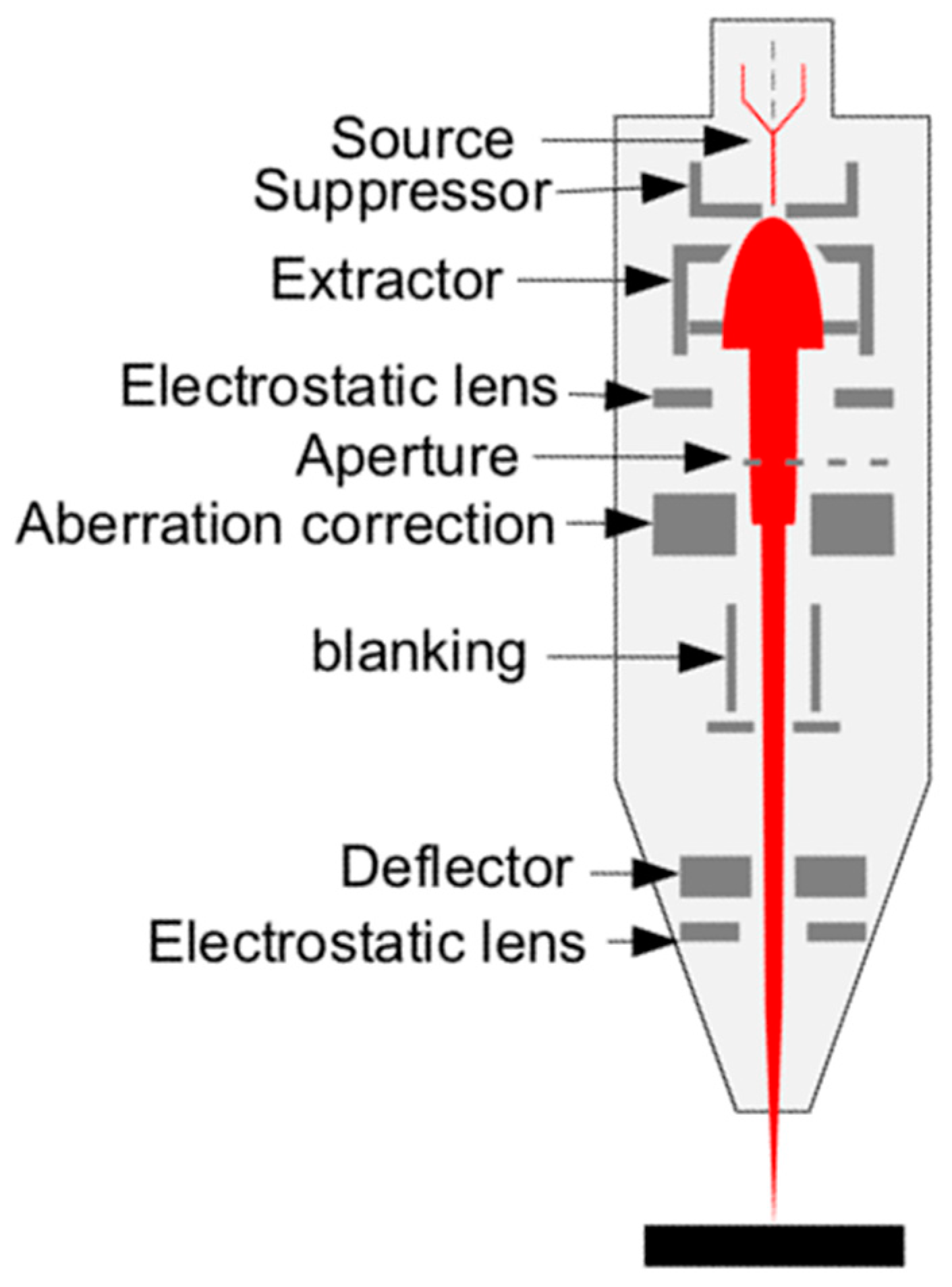
Figure 2. FIB ion optical column.
Advances in the ion source and ion optical column have greatly improved the performance of FIB systems. For a modern commercial Ga LMIS FIB, the beam current ranges from several pA up to 100 nA and the beam diameter at the sample is less than 5 nm. The first commercial GFIS helium ion microscope (HIM) was launched by Zeiss in 2007, and it can realize an ultra-high processing resolution of 0.25 nm at the low current down to 0.1 pA [11][12]. Thermo Fisher SCIENTIFIC (Waltham, MA, USA) Xe (ICP)–FIB can now achieve a resolution of less than 20 nm (30 kV) at the coincidence for Helios 5 PFIB. Orsay physics released a Xe plasma source in 2011 and TESCAN (Brno, Czech Republic) launched the fourth generation FIB of Xe+ (ECR), achieving a resolution of 15 nm at 30 keV. Compared to Ga+ FIBs, He+ FIBs have better contrast [13] with less sample damage and a slower processing speed. Plasma source systems are well-suited for large-volume/large-area milling of up to hundreds of cubic microns [14][15], as their maximum probe current can reach 2 uA and they can process samples 50 times faster than Ga+ FIBs.
2. FIB Operating Modes
The nature of a FIB’s multi functions (milling, deposition, and implantation) originates from ion–sample interaction, where the collision process involves a series of physical and chemical reactions and the collision depth depends mainly on the ion energy. The main reactions include: (1) the sputtering of neutral atomic or molecules (fragments or clumps) in the form of positive or negative ions, (2) ion implantation or energy deposition, (3) a crystallization change (surface atoms gain momentum and move from their original position, leaving vacancies), (4) secondary ion sputtering, (5) secondary electron emission (for each incident ion, a secondary electron yield is about 10–1000 times more than a secondary ion one [16]), (6) heating (usually diffusing radially, longitudinally, or at multiple angles from the point of incidence), (7) photo emission, (8) incident ion backscattering, and (9) chemical reactions that involve the breaking of chemical bonds, thereby dissociating gas molecules (this effect can be utilized during film deposition). Based on the ion–solid interaction, a FIB can achieve milling, deposition, and ion implantation.
3. FIB Equipment with Other Systems
As the mass of an ion is very large, some problems appear, such as a lower imaging resolution than SEM and sample damage, especially in crystal surfaces, existing in a single FIB system. In order to solve the above problems, other systems were induced to form dual-beam and multi-beam equipment.
3.1. FIB-SEM Dual-Beam System
Together with the in situ and real-time monitoring of SEM images, a FIB-SEM synchronization system maximizes the advantages of both ion and electron beams. As for the current SEM with Schottky Field Gun, it can last for 2000 h. Normally, a FIB-SEM synchronization system in a lab can work for more than 2 years without changing the ion source or the cathode. Two optical cylinders are typically connected at an angle of 50–60°, as shown in Figure 3. SEM can not only in situ monitor, but also neutralize ions to reduce the charge accumulation during FIB processing [17]. Moreover, 3D reconstructions can be performed by combing FIB repeatedly cutting cross-sections with SEM real-time imaging and the image processing software. Recent advances in FIB-SEM have enabled 3D reconstruction at a glancing angle, reducing image deformity due to tilt and providing more accurate representations of material structures. It has been successfully applied to the volume distribution of carbide in steel, crack tip analyses, the orthogonal cross-section characterization of tensile materials, carbon-based materials, bone hierarchical structures, proton exchange membrane (PEM) fuel cells, and so on [18][19]. Plasma FIB-SEM has emerged as a promising method for large-area milling, high-flux preparation with a low implantation layer, and high-throughput cryo-electron tomography. The use of plasma sources (e.g., Ar+ and Xe+) can achieve the 3D reconstruction of a larger area and volume of biomaterials [20][21]. Additionally, FIB-SEM is widely used in the characterization of material composition and 3D microanalyses, by combining with a mass spectrometer [22][23].
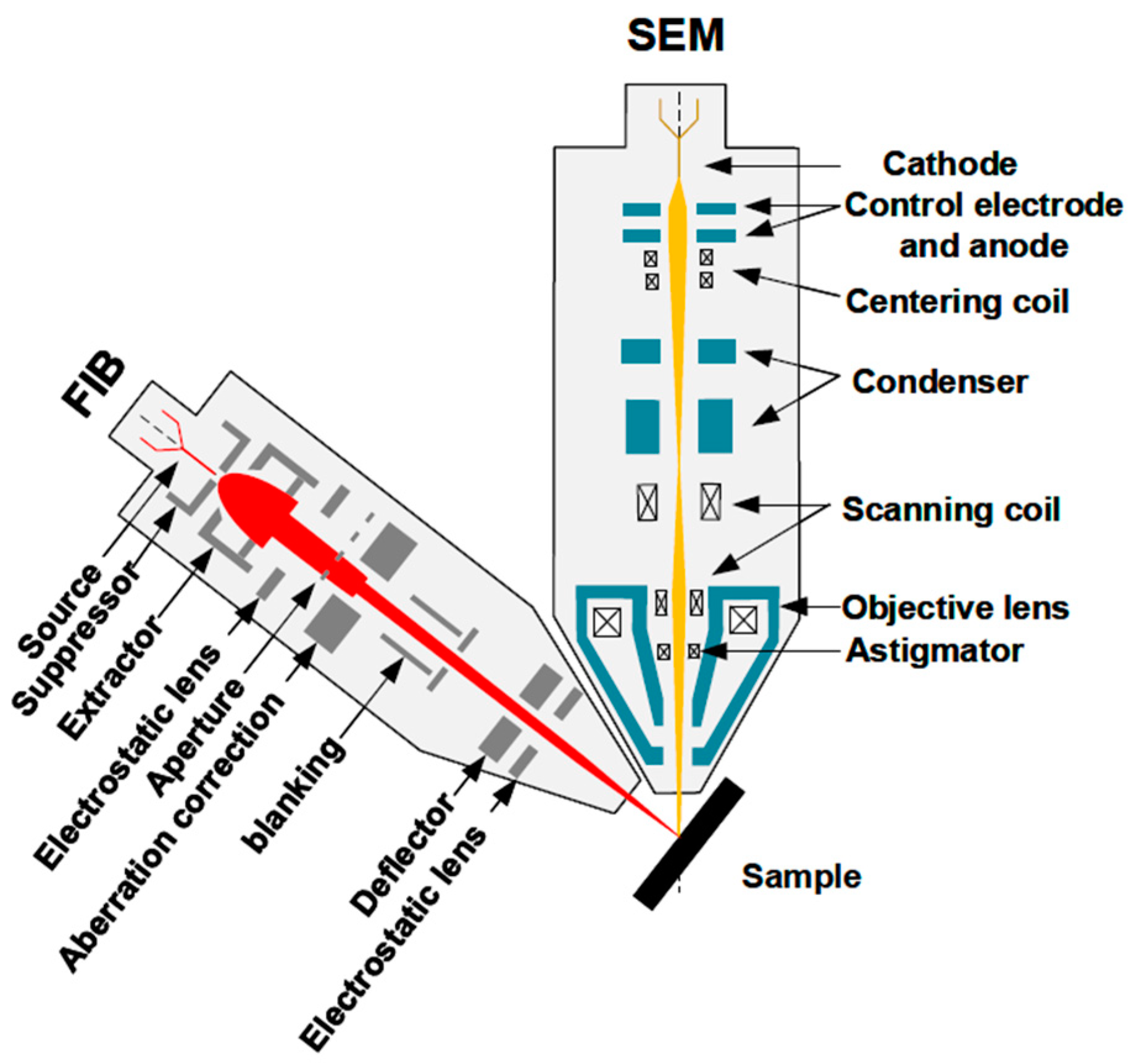
Figure 3. FIB-SEM dual-beam system.
The traditional preparation methods for bulk TEM samples are mechanical thinning, electrolytic polishing, and the ion milling technique [5], and their low success rate limits the application of TEM. FIB technology effectively improves the success rate of TEM sampling up to 95% by combining real-time SEM monitoring and a nanomanipulator [24]. Combining with thinning technology, the quality of TEM sample preparation can be further improved by choosing a lower FIB energy, a low-voltage and low-angle broad ion beam, and plasma FIB-SEM [25]. Additionally, an optional TEM column can be mounted to realize in situ TEM observation. An improved STEM/TEM alloy sample can be achieved using Xe+ plasma FIB milling with less damage during ion implantation [26]. For ceramic materials with a high strength, high melting point, and poor toughness, ion beam thinning may cause damage such as cracks or holes, which will be exacerbated with heat accumulation on the surface. Therefore, it is necessary to thin the sample at a low rate with a low incidence angle and the appropriate ion energy (varying from material to material) [27].
In situ performance measurements can also be achieved by combining FIB-SEM with other attachments to fully understand and master the properties of nanomaterials. Micro heating plate devices can provide a stable and controllable environment for investigating materials at different temperatures, allowing for in situ observations of the thermal behavior, phase transformations, and crystallography and composition changes [28]. High density and uniformity in material preparations such as metals, ceramics, and composite materials can be obtained using in situ spark plasma sintering (SPS) technology with uniform heating and rapid cooling. The mechanisms of phase evolution during the sintering process can be achieved by integrating in situ SPS technology [29]. Combined with electron beam (EM) technology, the range of FIB applications has been greatly expanded for micro–nano electromechanical systems (MEMS/NEMS), site-specific device production, IC repairment, and complex TEM sample preparation [5][30][31][32]. In early FIB-SEM systems, FIB and SEM worked by switching, as the magnetic field of the SEM objective lens would affect the performance of the FIB greatly. A FIB-SEM synchronization system was developed by solving the magnetic leakage and it could realize the in situ and real-time high-resolution monitoring of FIB fabrication.
3.2. Multi-Beam System
Based on the FIB-SEM dual-beam system, a multi-beam system has been developed to reduce sample damage. The triple-beam system of FIB-SEM-Ar can switch in different multiple ion sources. Hitachi (Tokyo, Japan) released the NX9000 with a selective add-on Ar ion column on FIB(Ga)-SEM in 2012, which effectively reduces this sample damage, as the damage thickness is only 2 nm for Ar+ instead of 10–30 nm for Ga+. Triple-beam technology realizes a continuous operation from high-precision FIB processing to Ar ion beam “cleaning” on one instrument, and greatly improves the sample preparation accuracy and reliability [33].
To further enhance the processing capacity of FIBs, Carl Zeiss implemented a multi-beam ion microscope named ORION NanoFab based on HIM, which integrated Ga, Ne, and He ion sources. He and Ne share the same ion optical column to achieve fast switching. The nominal probe sizes of Ga+, Ne+, and He+ are 3.0, 1.9, and 0.5 nm, respectively [34]. ORION NanoFab has been successfully applied in magnetic materials, biology materials, and insulative materials, which has obtained graphene with direct-write features as small as 5 nm [35], surface plasma antennas with a tip gap of 4 nm [36], and line patterns with the line edge of 1.81 ± 0.06 nm and the width roughness of 2.90 ± 0.06 nm on Ni-based metal−organic clusters [37].
Compared to multi-beam systems, FIB-SEM dual-beam systems are more affordable. With advantages of a high precision, multi functions, and in situ real-time monitoring, FIB-SEM synchronization systems are expected to achieve the 3D controllable fabrication of nanomaterials.
References
- Stevie, F.; Giannuzzi, L.; Prenitzer, B. The Focused Ion Beam Instrument. In Introduction to Focused Ion Beams: Instrumentation, Theory, Techniques and Practice; Springer Science & Business Media: Berlin, Germany, 2005; pp. 1–12.
- Smith, N.S.; Notte, J.A.; Steele, A.V. Advances in source technology for focused ion beam instruments. MRS Bull. 2014, 39, 329–335.
- Smith, N.S.; Skoczylas, W.P.; Kellogg, S.M.; Kinion, D.E.; Tesch, P.P.; Sutherland, O.; Aanesland, A.; Boswell, R.W. High brightness inductively coupled plasma source for high current focused ion beam applications. J. Vac. Sci. Technol. B Microelectron. Nanometer Struct. Process. Meas. Phenom. 2006, 24, 2902–2906.
- Liu, Z.; Sun, G.; Zhang, D.; Chen, J.; Zhong, G.; Chuan, G. Characteristics of an electron cyclotron resonance plasma source. Nucl. Tech. 2000, 23, 707–712.
- Zhang, Z.; Wang, W.; Dong, Z.; Yang, X.; Liang, F.; Chen, X.; Wang, C.; Luo, C.; Zhang, J.; Wu, X.; et al. The Trends of In Situ Focused Ion Beam Technology: Toward Preparing Transmission Electron Microscopy Lamella and Devices at the Atomic Scale. Adv. Electron. Mater. 2022, 8, 2101401.
- Prosa, T.J.; Larson, D.J. Modern Focused-Ion-Beam-Based Site-Specific Specimen Preparation for Atom Probe Tomography. Microsc. Microanal. 2017, 23, 194–209.
- Lee, H.-T.; Kim, H.-J.; Kim, C.-S.; Gomi, K.; Taya, M.; Nomura, S.; Ahn, S.-H. Site-specific characterization of beetle horn shell with micromechanical bending test in focused ion beam system. Acta Biomater. 2017, 57, 395–403.
- Li, W.-P.; Han, L.; Gu, W.-Q. Design of practical deflection field in nanometer-scale focused ion beam system. Nucl. Instrum. Methods Phys. Res. Sect. A Accel. Spectrometers Detect. Assoc. Equip. 2007, 579, 937–940.
- Nee, A.Y.C. Manufacturing Engineering and Technology; Springer: Berlin/Heidelberg, Germany, 2014.
- Klingner, N.; Hlawacek, G.; Mazarov, P.; Pilz, W.; Meyer, F.; Bischoff, L. Imaging and milling resolution of light ion beams from helium ion microscopy and FIBs driven by liquid metal alloy ion sources. Beilstein J. Nanotechnol. 2020, 11, 1742–1749.
- Belianinov, A.; Burch, M.J.; Kim, S.; Tan, S.; Hlawacek, G.; Ovchinnikova, O.S. Noble gas ion beams in materials science for future applications and devices. MRS Bull. 2017, 42, 660–666.
- Stanford, M.G.; Lewis, B.B.; Mahady, K.; Fowlkes, J.D.; Rack, P.D. Review Article: Advanced nanoscale patterning and material synthesis with gas field helium and neon ion beams. J. Vac. Sci. Technol. B 2017, 35, 030802.
- Bassim, N.; Scott, K.; Giannuzzi, L.A. Recent advances in focused ion beam technology and applications. MRS Bull. 2014, 39, 317–325.
- Burnett, T.L.; Kelley, R.; Winiarski, B.; Contreras, L.; Daly, M.; Gholinia, A.; Burke, M.G.; Withers, P.J. Large volume serial section tomography by Xe Plasma FIB dual beam microscopy. Ultramicroscopy 2016, 161, 119–129.
- Burnett, T.L.; Winiarski, B.; Kelley, R.; Zhong, X.L.; Boona, I.N.; McComb, D.W.; Mani, K.; Burke, M.G.; Withers, P.J. Xe+ Plasma FIB: 3D Microstructures from Nanometers to Hundreds of Micrometers. Microsc. Today 2016, 24, 32–39.
- Nezri, E.; Orloff, J. Neutrino Oscillations v.s. Leptogenesis in SO(10) Models. J. High Energy Phys. 2003, 2003, 1–20.
- Luo, H.; Jing, R.; Cui, Y.-M.; Wang, H.-L.; Wang, R.-M. Improvement of fabrication precision of focused ion beam by introducing simultaneous electron beam. Prog. Nat. Sci. Mater. Int. 2010, 20, 111–115.
- Shojaeefard, M.H.; Molaeimanesh, G.R.; Nazemian, M.; Moqaddari, M.R. A review on microstructure reconstruction of PEM fuel cells porous electrodes for pore scale simulation. Int. J. Hydrogen Energy 2016, 41, 20276–20293.
- Nan, N.; Wang, J. FIB-SEM Three-Dimensional Tomography for Characterization of Carbon-Based Materials. Adv. Mater. Sci. Eng. 2019, 2019, 8680715.
- Rigort, A.; Kotecha, A.; Reyntjens, S.; Mitchels, J. A Next Generation Cryo-FIB Microscope for High-Throughput Cryo-Electron Tomography. Microsc. Microanal. 2022, 28, 1250–1251.
- Dumoux, M.; Glen, T.; Smith, J.L.; Ho, E.M.; Perdigão, L.M.; Pennington, A.; Klumpe, S.; Yee, N.B.; Farmer, D.A.; Lai, P.Y. Cryo-plasma FIB/SEM volume imaging of biological specimens. Elife 2023, 12, e83623.
- Pillatsch, L.; Östlund, F.; Michler, J. FIBSIMS: A review of secondary ion mass spectrometry for analytical dual beam focussed ion beam instruments. Prog. Cryst. Growth Charact. Mater. 2019, 65, 1–19.
- Audinot, J.-N.; Vollnhals, F.; Gratia, P.; Eswara, S.; Philipp, P.; Wirtz, T. Secondary Ion Mass Spectrometry on the Helium Ion Microscope: Methodologies for analysis of nanomaterials. Microsc. Microanal. 2018, 24, 1016–1017.
- Giannuzzi, L.A.; Stevie, F.A. A review of focused ion beam milling techniques for TEM specimen preparation. Micron 1999, 30, 197–204.
- Knipling, K.E.; Rowenhorst, D.J.; Fonda, R.W.; Spanos, G. Effects of focused ion beam milling on austenite stability in ferrous alloys. Mater. Charact. 2010, 61, 1–6.
- Zhong, X.L.; Wade, C.A.; Withers, P.J.; Zhou, X.; Cai, C.; Haigh, S.J.; Burke, M.G. Comparing Xe+ pFIB and Ga+ FIB for TEM sample preparation of Al alloys: Minimising FIB-induced artefacts. J. Microsc. 2020, 282, 101–112.
- Huh, Y.; Hong, K.J.; Shin, K.S. Amorphization Induced by Focused Ion Beam Milling in Metallic and Electronic Materials. Microsc. Microanal. 2013, 19, 33–37.
- Novák, L.; Wu, M.; Wandrol, P.; Kolíbal, M.; Vystavěl, T. New approaches to in-situ heating in FIB/SEM systems. Microsc. Microanal. 2017, 23, 928–929.
- Papynov, E.K.; Portnyagin, A.S.; Modin, E.B.; Mayorov, V.Y.; Shichalin, O.O.; Golikov, A.P.; Pechnikov, V.S.; Gridasova, E.A.; Tananaev, I.G.; Avramenko, V.A. A complex approach to assessing porous structure of structured ceramics obtained by SPS technique. Mater. Charact. 2018, 145, 294–302.
- Orús, P.; Sigloch, F.; Sangiao, S.; De Teresa, J.M. Superconducting materials and devices grown by focused ion and electron beam induced deposition. Nanomaterials 2022, 12, 1367.
- Tai, K.; Li, Y.; Liu, S.; Guo, Z.; Li, C.; Du, L.; Zhao, S.; Li, X.; Liu, J. In Situ FIB-TEM-TOF-SIMS Combination Technique: Application in the Analysis of Ultra-Light and Trace Elements in Phyllosilicates. Minerals 2022, 12, 562.
- Minenkov, A.; Šantić, N.; Truglas, T.; Aberl, J.; Vukušić, L.; Brehm, M.; Groiss, H. Advanced preparation of plan-view specimens on a MEMS chip for in situ TEM heating experiments. MRS Bull. 2022, 47, 359–370.
- Tiddia, M.; Seah, M.P.; Shard, A.G.; Mula, G.; Havelund, R.; Gilmore, I.S. Argon cluster cleaning of Ga+ FIB-milled sections of organic and hybrid materials. Surf. Interface Anal. 2018, 52, 327–334.
- Allen, F.I.; Velez, N.R.; Thayer, R.C.; Patel, N.H.; Jones, M.A.; Meyers, G.F.; Minor, A.M. Gallium, neon and helium focused ion beam milling of thin films demonstrated for polymeric materials: Study of implantation artifacts. Nanoscale 2019, 11, 1403–1409.
- Zhang, W.; Zhang, Q.-H.; Zhao, M.-Q.; Theil Kuhn, L. Direct writing on graphene ‘paper’ by manipulating electrons as ‘invisible ink’. Nanotechnology 2013, 24, 275301.
- Kollmann, H.; Piao, X.; Esmann, M.; Becker, S.F.; Hou, D.; Huynh, C.; Kautschor, L.-O.; Bosker, G.; Vieker, H.; Beyer, A.; et al. Toward plasmonics with nanometer precision: Nonlinear optics of helium-ion milled gold nanoantennas. Nano Lett. 2014, 14, 4778–4784.
- Kumar, R.; Chauhan, M.; Moinuddin, M.G.; Sharma, S.K.; Gonsalves, K.E. Development of Nickel-based Negative Tone Metal Oxide Cluster Resists for sub-10 nm Electron Beam and Helium Ion Beam Lithography. ACS Appl. Mater. Interfaces 2020, 12, 19616–19624.
More
Information
Subjects:
Physics, Applied
Contributors
MDPI registered users' name will be linked to their SciProfiles pages. To register with us, please refer to https://encyclopedia.pub/register
:
View Times:
3.4K
Revisions:
2 times
(View History)
Update Date:
21 Jun 2023
Table of Contents


Notice
You are not a member of the advisory board for this topic. If you want to update advisory board member profile, please contact office@encyclopedia.pub.
OK
Confirm
Only members of the Encyclopedia advisory board for this topic are allowed to note entries. Would you like to become an advisory board member of the Encyclopedia?
Yes
No
${ textCharacter }/${ maxCharacter }
Submit
Cancel
Back
Comments
${ item }
|
${ item.createdUser.fullName }
${ item.createdAt }
${ item.vote }
${ item.reply }
Delete
${ reply.createdUser.fullName }
${ reply.createdAt }
${ reply.vote }
Delete
There is no reply to this comment~
${ item.replyTextCharacter }/${ item.replyMaxCharacter }
Submit
Cancel
More
No more~
There is no comment~
${ textCharacter }/${ maxCharacter }
Submit
Cancel
${ selectedItem.replyTextCharacter }/${ selectedItem.replyMaxCharacter }
Submit
Cancel
Confirm
Are you sure to Delete?
Yes
No