1. Introduction
Ionizing radiation refers to charged (α and β particles, and protons) and uncharged (neutrons) particles or electromagnetic radiation (X-rays and γ-rays) that have enough energy to ionize atoms or molecules by detaching electrons from them. Cosmic rays are also ionizing radiation. They are not a single class of particles, but a large group that contains, in addition to these, others not belonging to ordinary matter, such as muons or pions. However, cosmic rays will not be considered in this review. Neutrons are indirect ionizing radiation because they do not interact directly with electronic shells, but rather with atomic nuclei. However, several ionizing radiations are generated by these interactions so that matter ionization occurs via intermediate particles. In Figure 1 the most common ionizing particles are shown. Alpha particles or alpha rays are helium nuclei that have a big charge and mass. Therefore, they have a small capacity to penetrate matter and, for this reason, they mainly create many localized defects. Beta particles are electrons (β-) or positrons (β+) emitted by radioactive nucleides. They are about 7300 times lighter than the alpha particle, and therefore have a greater ability to penetrate matter. Along their path, they can generate γ and X-rays. High-energy photons (γ-rays and X-rays) have zero mass and therefore large penetration ability. Along their path in a material they can generate secondary particles and other lower energy photons. Protons belong to an intermediate case between alpha and beta particles, i.e., their mass is about four times smaller than that of alpha particles and therefore their penetration capacity is larger than that of alpha particles. They can generate secondary particles themselves. Neutrons differ from protons, although they have similar masses, because they have no electric charge and for this reason they have high penetration capacity, depending on their own energy. It is worth keeping in mind that four classes of neutrons are commonly classified based on their initial energy Ei: thermal (Ei < 0.025 eV), epithermal (Ei 0.025 eV–100 keV), fast (Ei 100 keV–20 MeV), and high energy (Ei> 20 MeV).
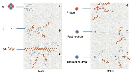
Figure 1. Scheme of the interaction with matter of ionizing particles: (a) α particle. (b) β particle. (c) x and γ-rays. (d) proton. (e,f) fast and thermal neutron, respectively. Neutron matter interaction probability is higher at low energies (thermal or cold neutrons), whereas high energy neutrons (fast) have only a few interactions. Thermal neutrons are much more scattered by atomic nuclei than fast neutrons, so that for the same material, the mean free path is short for thermal neutrons, whereas fast ones are able to penetrate for longer distances.
2. Radiation–Matter Interaction
Matter can interact with different types of particles, namely electromagnetic radiation (X-rays and γ-rays), charged particles (α and β particles, protons), and uncharged particles (neutrons). Thus the interaction of radiation with a material has to be described differently, depending on the type of particle involved in the interaction. In this review, devices for the detection of X-rays, neutrons, and protons are reported, therefore only the interactions of these particles with matter will be described. Moreover, only interactions with solid materials will be discussed here, because they are related to perovskite-based detectors.
An X-ray or
γ-ray photon incident on the detector can interact with the electrons or with the nuclei of the material constituting the detector. The transfer of energy from the incident photon to the detector material can mainly occur in three different ways: Compton scattering, photoelectric absorption, and pair production
[1], each of which is predominant in a certain energy range, which also depends on the atomic number of the element involved. Schematically, it can be said that the photoelectric effect is prevalent at relatively low energies, the Compton effect for intermediate energies and the pair production at higher energies.
The Compton effect occurs when the incident photon is scattered by the outer shell electron and a portion of the photon energy is transferred to the scattered electron. The complete absorption of the high-energy photon by an electron of the inner shell is the photoelectric absorption, since a photoelectron is produced with kinetic energy equal to the energy of the photon minus the binding energy of the electron. The production of a pair results in the generation of an electron-positron pair after the incident photon has been absorbed by the strong Coulomb electric field near the nuclei. Therefore, it can only occur when the energy of the photon is larger than the rest energy of the electron-positron pair, that is 1.022 MeV. Secondary electrons, including photoelectrons containing the full energy of the absorbed photons, scattered electrons, containing a fraction of the energy of the scattered photons, and electron-positron pairs can participate in a variety of both elastic and inelastic scattering events, which will convert their kinetic energy into a discrete number of electron–hole pairs. This number is calculated by dividing the total energy by the creation energies (in the range of a few eV) of the electron–hole pairs
[2][3]. The cross sections of all three interactions increase with atomic number (Z). Therefore, high-Z materials are preferred, especially for the detection of high-energy X-rays and
γ-rays which, in common detectors, can penetrate from millimeters to centimeters. The internal conversion is similar to the photoelectric effect: in this case the high-energy photon strips an electron from a deep shell from the atom. A second electron of a higher energy level fills the hole created by emitting a lower energy photon in the process.
-
Scattering: Neutrons may collide with nuclei and undergo either elastic or inelastic scattering. In the former case, a neutron transfers a fraction of its kinetic energy to the target nucleus without exciting the nucleus, whereas inelastic scattering occurs when the neutron transfers some of its kinetic energy to the target nucleus, by which the target becomes excited and the excitation energy is emitted as a γ-rays.
-
Absorption: When a target nucleus absorbs a neutron, a wide range of nuclear reactions occur, including nuclear fission (this is more favorable at thermal energies): Radiative capture occurs when a neutron is absorbed by the target nucleus which then becomes excited and reaches stability by emission of electromagnetic energy in a form of γ-rays. Transmutation occurs when the target nucleus absorbs a neutron that results in an ejection of a charged particle such as a proton or an alpha particle. Nuclear fission reaction occurs when a fissile nucleus (this phenomenon concerns above all very heavy elements such as uranium or plutonium) splits into smaller nuclei (fission fragments). As the fission fragments are ejected, an average of 2.5 neutrons are emitted. In this way, a neutron can collide with another fissile nucleus which then splits into smaller nuclei and a reaction chain can take place, as in a nuclear power plant. Thermal neutrons are much more effective for the fission. In each scattering event, the neutrons lose some of their energy and eventually the fast neutrons slow down to being thermal neutrons.
Neutron detection mainly depends on elastic scattering with nuclei. Capture cross sections are small for most materials, with a single exception represented by thermal neutrons (E < 1 eV), which can be effectively captured by a few specific nuclei, such as
3He,
10B,
6Li and
157Gd, through nuclear reactions. These reactions produce secondary emissions which include protons,
α and
β particles and electromagnetic radiation
[4]. Instead, in the case of fast neutrons, the interaction consists of elastic diffusion and since the hydrogen nucleus has the same mass as the neutron, it becomes the most effective energy degrader. The recoil nucleus, which in the case of hydrogen is the proton, transfers its energy to the surrounding electrons in a short range, similarly as an
α particle.
Protons can also interact with matter in many ways with rather complex mechanisms (Figure 1b). It must be taken into account in this case that they are charged particles and therefore they can interact with both atomic nuclei and electron shells. Even proton Bremsstrahlung is theoretically possible, but generally is negligible. They can act directly as ionizing particle via inelastic Coulombic interactions, losing energy that releases an electron; they can undergo to a deflection of their trajectory by repulsive Coulomb elastic scattering with nucleus; they can have non-elastic nuclear interaction with the formation of secondary particles, such as neutrons, γ-rays and lower energy protons.
Proton therapy offers a substantial clinical advantage over conventional photon therapy, due to the unique depth-dose characteristics of protons, which can be exploited to achieve significant reductions in normal tissue doses proximal and distal to the target volume. These may allow a more accurate sparing of normal tissues, potentially improving local control and survival. In contrast to photons, when protons of a given energy (typically in the range of 70 to 250 MeV) penetrate matter, they slow down continuously as a function of depth. The rate of their energy loss (called “linear energy transfer” or LET) increases with decreasing velocity. This continues until their entire energy is depleted and then they come to an abrupt stop. This process of dose deposition produces a characteristic depth-dose curve called “Bragg curve”: the point of highest dose corresponds to the Bragg peak, the depth of the peak, the proton range, is a function of the initial energy. By tuning the energy of the beam, the Bragg peak may be focused at the tumor, to improve spatial accuracy in dose delivery and thus spare healthy surrounding tissues. Dosimetric systems in proton therapy are used to support treatment plans, by taking into account parameters as proton fluxes, dose-rates, beam angles, and patient positioning aspects required to deliver an appropriate dose to the target volume.
3. Radiation Detection
Radiation detection relies on partial or complete energy transfer from photons/particles to the detector material. The operating principle of all radiation detectors is the same: they convert radiation into optical or electrical signals which can subsequently be amplified and processed by conventional electronics. In addition to specific radiation requirements, detectors must meet some common requirements: they must have a high absorption cross section, as well as a high charge carrier/photon conversion efficiency, low noise, high spatial and timing resolutions, and high radiation hardness.
Based on their operating mechanisms, radiation detectors can be classified into different categories: solid-state detectors, i.e., with direct conversion, scintillators, liquefied noble gas detectors, and gaseous ionization detectors, which are indirect conversion detectors. In this review only the first category will be discussed.
4. Radiation Detectors: Brief Overview
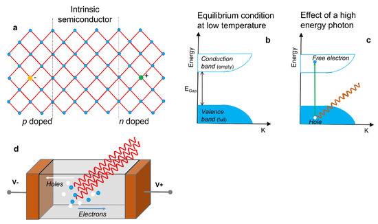
Solid-state detectors provide a signal by collecting the current generated by the charge liberated in the passage of the particle through a semiconductor. As shown in Figure 2a, semiconductors can be intrinsic, p-doped, or n-doped (if some atoms in the lattice are replaced by hetero-elements with fewer or more electrons than the parent element, respectively). For the function of a detector, high purity materials are required. At low temperature, from an electronic point of view, the system is described by the scheme of the semiconductor band structure of Figure 2b. A high-energy photon can excite an electron, making it jump from the valence band to the conduction one (Figure 2c). In this way an electron–hole pair is generated, capable of carrying electric current. Electrons and holes have opposite polarities so they move in opposite directions under the action of an electric field. Under the action of gamma rays, numerous electron–hole pairs are generated in the semiconductor. A picture showing the operating mechanisms of a X-ray detector is reported in Figure 2d. The peak current that can be measured is proportional to the intensity of the gamma ray beam.
Figure 2. (a) Sketch of an intrinsic semiconductor, a p-doped and a n-doped semiconductor. (b) Condition of equilibrium of the semiconductor bands. (c) Effect of a high-energy photon incident on the semiconductor with the creation of an electron–hole pair. (d) Operating mechanisms of a solid-state X-ray detector, where electrons and holes are driven by the electric field and collected by the contacts.
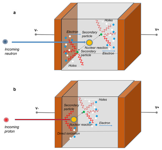
The operating mechanisms of a solid-state detector for neutrons and protons is shown in Figure 3. Neutrons have a higher penetration capacity than protons, but they do not directly ionize matter. Only particles that are generated due to one of the nuclear processes described above induce ionization. A cloud of electron and hole particles is produced, initially it is more localized (Figure 3a). Instead, the effects of a beam of protons on matter are numerous, as previously described. They can directly ionize matter along their path or generate a nuclear process. As a consequence, a cloud of electrons and holes can be created, however it is very localized, due to the limited mean free path of the protons (Figure 3b).
Figure 3. Operating mechanisms of a solid-state detector for the detection of neutrons (a) and protons (b). Secondary electrons and holes are generated by the interaction of the primary particle (neutron or proton) with the active medium of the detector. Protons can also directly ionize matter along their path. Anyhow, the so generated electrons and holes are driven by the electric field and collected by the contacts.
In a solid-state detector the electron–hole pairs generated by the incident photons or particles induce an electrical signal at electrodes. As will be explained in more detail in the next paragraph, to facilitate charge transport and maximize charge collection efficiency, detector materials should have the so-called “mobility-lifetime product” (μτ product) large enough to allow electrons or holes to travel through the detector and get to the contacts. Furthermore, to minimize the leakage current under a large electric field, the bandgap of the detector materials must be relatively large and the defect densities should be opportunely controlled along the entire device structure.
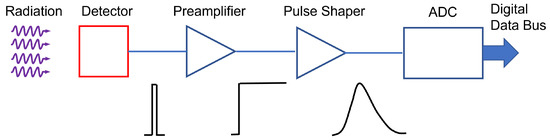
A basic radiation detection chain is shown in Figure 4.
Figure 4. Sketch describing the steps of a basic radiation detection chain.
Incident radiation releases energy in the sensing material. The conversion of the energy deposited by radiation to an electrical signal can be achieved in different ways. In the case of a semiconductor sensor, electron–hole pairs are created in a number proportional to the absorbed energy. To establish the electric field, a potential is applied between the electrodes, to accelerate the generated charge carriers. They are swept by the applied electric field causing an induced charge on the opposite electrodes, as predicted by the Shockley–Ramo theorem
[5][6]. This low-level electrical signal is initially sent to a pre-amplifier stage, which has also the function of integrating the signal; it is then fed to a pulse-shaper and finally it is digitized for storage and analysis.
Although the primary physical quantity measuring the signal energy is the charge, when the pulse shape is the same for all signal magnitudes, the pulse amplitude, called “pulse height” may be considered a more convenient parameter. This “pulse height analysis”, gives as output the pulse height spectrum, or energy spectrum.
The detector signal may be collected either in pulse- or current-mode, depending on the specific application. The output of the pulse-mode detector is a train of voltage pulses, each corresponding to a detected particle: it may be thus regarded as a single-event process. The voltage signal is then amplified and collected as a histogram through a shaping amplifier and a multichannel analyzer. Under current-mode operation, instead, during irradiation the current signal at a constant applied voltage is integrated on selected sampling intervals and read-out within fixed intervals as a function of time.
The performance of a radiation detector in general is measured in terms of parameters as gain, response time, signal to noise ratio, sensitivity.
In general, the read-out charge signal Qs is proportional to the absorbed energy E through the relationship (1):
where E is the absorbed energy, Ei the energy required to form a charge pair, and q is the electronic charge. The ionization energy Ei is proportional to the bandgap, Eg, so that higher bandgap materials yield less signal charge. The relationship between Ei and Eg has been studied extensively in literature. Klein [7] calculated the average amount of radiation energy consumed per pair as a sum of three contributions: the bandgap, optical phonon losses, and the residual kinetic energy as 95Eg. Nonetheless, Ei mean-ionization energies smaller than those predicted by the Klein’s relationship have been observed in various halide semiconductors as e.g., perovskites [2]. An empirical model developed by Devanathan et al. [8] includes these deviations suggesting the following relationship (2) of Ei vs bandgap:
The sensitivity per unit active volume of the semiconductor materials is then defined as:
Sv=qρ/Ei, with
ρ mass density
[9]. In general, lower bandgap semiconductor materials are characterized by lower ionization energies, thus providing higher concentrations of generated e–h pairs and consequently higher signals. On the other hand, higher bandgap semiconductors allow for a negligible thermal generation of e–h pairs, thus a reduced noise from leakage current during exposure to radiation.
For this reason, semiconductors with intermediate gaps, typically in the range 1–3 eV are considered, as e.g., Si and SiC, with sensitivity per unit volume of 637 nCGy−1mm−3 and 411 nCGy−1mm−3, respectively, where Gy is the unit of dose (1 Gy= 1 J/kg). In a detector working as a dosimeter, an important requirement is that the collected charge/current signal should be linear functions of the dose/dose-rate. The slope of such linear functions is the sensitivity of the device S, expressed usually in nC/Gy. In segmented dosimeters, used to imaging the dose on a bidimensional map, it is also quite important to evidence the sensitivity per unit active area for each pixel, a parameter expressed as nCGy−1mm−2.
The semiconductor sensor may operate either as a photoresistance or as a p-n device. The latter structure is particularly useful to achieve high signal-to-noise ratios and fast responses, due to the presence of a depleted region at the interface of the two differently doped regions. This is especially important when the gap of the material is low, as in Ge or Si, as the thermally generated free carrier concentrations in the semiconductor are of the same order or higher than the concentration of e–h pairs generated by the impinging radiation. Assuming a photodiode under partial depletion, and a radiation-induced uniform generation of e–h pairs throughout the semiconductor, those carriers generated in the junction region will be swept across the junction by the electric field and collected within a few nanoseconds. Charged carriers created outside the depletion region will cause a transient increase in the local carrier density, giving rise to an adding current contribution. This will appear as a delayed component to the current signal, due to the longer time required for carriers to diffuse to the junction from the neutral bulk. This contribution is in fact proportional to the minority diffusion length L=√(Dτ), with D diffusivity and τ minority carrier lifetime. To fasten and maximize the signal it is thus convenient to increase the depleted depth of the photodiode up to the physical total thickness of the device by increasing the externally applied reverse voltage (this practice, in case of high doping and thin devices, may actually be limited by unwanted breakdown effects.).
Conversely, a photoconductor consists of a slab of semiconductor, in bulk or thin-film form, with ohmic contacts either at opposite ends or interdigitated. When incident radiation falls on the surface of the photoconductor, carriers are generated, resulting in an increase of the electrical conductivity. Considering a steady flow of photons impinging uniformly on the surface of an extrinsic photoconductor with intercontact distance
d, the photocurrent gain of the device is defined
[10] as:
where μ is the carrier mobility, τ is the carrier lifetime and ε the applied electric field. In a semiconductor, the total induced charge is given by the sum of the induced charges due both to the electrons and holes. For a detector having a uniform electric field E there are two relevant μτ products for holes and electrons.
This ability of photoconductors to exhibit a photoconductive gain, so that the number of charge carriers that flow through the external circuit in response to the input signal can exceed the number of electron hole pairs generated by photon absorption, has drawbacks in longer temporal responses and potentially higher noise contributions with respect to photodiodes. In fact, the temporal response of this kind of device is directly related to the lifetime τ of the photogenerated e–h pairs. Moreover, the absence of a depleted region due to the ohmic configuration, may give rise to a non-negligible dark conductivity, due to the thermal generation of charged carriers, which may be particularly detrimental in small-bandgap materials.
For direct X-rays detectors, sensitivity is generally governed by X-ray attenuation, electron–hole pair generation, carrier extraction and photoconductive gain. For a given material, the capacity of attenuation and electron–hole pair generation energy are fixed, and thus the sensitivity is mainly dependent on carrier extraction and gain. The ability of carrier extraction can be determined by the mobility-lifetime (
μτ) product, which can be derived by fitting the photoconductivity using the Hecht Equation (4)
[11]:
where I0 is the saturated photocurrent, L is the thickness, V is the applied bias, t is the carrier lifetime. This situation may be in practice considered when using either a resistive device or a reverse biased p-i-n detector [12]. Modified Hecht’s expression for semi-insulating semiconductors where space charges may be present have been also reported, which apply in case native and radiation induced defects are influencing the carriers transport properties [13][14][15]. In this case, a generalized Hecht equation is considered, incorporating both types of carriers, starting from the Gunn theorem [16].
Photoconductivity gain is desirable for highly sensitive photodetectors. In principle, photodetectors with diode structures such as p–n junction, p–i–n junction, or Schottky junction diodes have no intrinsic gain. Under large bias voltage, there may be impact ionization induced avalanche gain, which can be ascribed to the accelerated electrons or holes colliding with atomic electron, usually happening under large electric field. This impact ionization effect has been extensively applied to increase the performances in conventional semiconductor detectors
[10]. However, semiconductors characterized by a heavily disordered lattice do not normally exhibit impact ionization. In fact, here carriers are more localized and charge transport occurs mainly through thermally activated hopping. As a result, it is difficult for carriers to accumulate sufficient kinetic energy to enable an avalanche effect. Nonetheless, a photoconductive gain may be observed indeed, which may originate by trapped carriers at defects, improving tunnelling injection at electrodes
[17].
5. Perovskite Detectors For X-rays
The interest in perovskite-based ionizing radiation detectors is quite recent, also considering that the first perovskite film-based X-rays detector was published in 2015 by Yakunin et al.
[18]. Since then, research has aimed to increase the thickness of the film, i.e., the absorption of the radiation, while maintaining a high
μτ in order to guarantee a high charge collection efficiency. Pressing and melting processes were often employed to obtain thick films and wafers
[19][20][21][22]. Hu et al.
[20] measured a high value of sensitivity per unit area of
1.22×10⁵ μCGy−1cm−2 in a perovskite film detector consisting of an 800
μm-thick MAPbI
3 wafer obtained by heat-assisted pressing. Kim et al.
[23], instead, using a solution-based technique, fabricated a highly efficient large-area MAPbI
3-based X-ray detector with thickness of 830
μm, allowing printing on a thin film transistor backplane of large area. The authors report a sensitivity per unit area of up to
1.1×10⁴ μCGy−1cm−2, a large value of the product
μτ of the charge carrier (
1.0×10⁻⁴ cm2V−1) and evaluated a rapid response to a train of short X-ray pulses with a pulse width of 50 ms. The highest value of sensitivity per unit area (
4.2×10⁵ μCGy−1cm−2) was achieved by Xiao et al.
[24], after grain engineering. The active medium of such ultra-sensitive perovskite X-ray detector was a 1.3 mm thick MAPbI
3 wafer obtained through hot pressing method.
Apart from a few cases of flexible devices consisting of a perovskite thick film
[25][26][27], in which the film thicknesses were anyhow less than a few tens of micrometres, or perovskite-filled membranes
[28], thick films or wafers generally did not lead themselves to the implementation of flexible devices. For this reason, many research works have recently focused on the synthesis and use of thin films as active media of radiation detectors. The first perovskite-based flexible X-ray detectors were demonstrated by Liu et al.
[29] in 2019. They printed a inorganic CsPbBr
3 quantum dots (QDs) solution onto pre-patterned metal electrodes on Si or flexible substrate in PET through the inkjet printing method. They obtained a photoconductor made of a 20 nm-thick perovskite layer. The authors observed a rapid response (rise time of about 30 ms) to X-rays at bias voltages below 1 V. The sensitivity value achieved by the flexible device was
17.7 μCGy−1cm−2 under soft X-ray-near UV synchrotron beamline (100–2500) eV, biased at 0.1 V, while the one for the rigid device was 83
μCGy−1cm−2 under same irradiation conditions. Despite the good X-ray detection performance, the photoconductor architecture and the QDs suspension brought trouble to material stabilization and transport control.
Halide perovskite film-based detectors for ionizing radiation have seen rapid development in recent years, especially for neutron and proton detection in the last couple of years. The advantages of halide perovskites are tunable compositions to meet the requirements of different types of radiation, low-cost and versatile deposition techniques for large-scale production, and excellent optoelectronic properties for efficient detection. Since 2015, the year of the development of the first detector for X-rays based on organic perovskite (MAPbI3), in order to increase the device efficiency. The first research focused on the investigation of techniques to increase the thickness. Then, new stoichiometries, also lead-free, and novel device architectures have been investigated. Recently, research has moved towards the study of flexible substrate detectors. Despite the promising results shown above, many efforts still need to be made to obtain high values of sensitivity per unit area of a detector implemented on a flexible substrate.
6. Perovskite Detectors for Neutrons
Solid-state neutron detection devices found in the literature are almost exclusively single crystals. However, Fernandez-Izquierdo et al. developed a cesium lead bromide (CsPbBr
3) thin-film-based indirect-conversion solid-state thermal neutron detector, where the perovskite thin film is combined with a
10B conversion film
[30]. In that work, the close space sublimation (CSS) method was used for the deposition of the perovskite film. The CSS process used small crystals as precursors to enable films with large columnar grain growth across the entire film thickness of 8–9
μm. The mechanism of detection is indirect, the neutron response is enabled by the low leakage current (around 10
−8 A mm
−2) and fast response of the Ga
2O
3/CsPbBr
3 diode. The efficiency reported for thermal neutrons is around 1%. By doping the surface of the perovskite layer with Cl anions coming from the treatment with PbCl
2 vapor, such efficiency value was further improved up to 2.5%. The same group reported an optimized microstructured material for thermal neutron detection with a combination of different techniques, such as a solvent-free thin-film deposition, perovskite patterning and dry etching process using HBr + Ar plasma. The fabricated microstructured CsPbBr
3 thermal neutron detectors showed an efficiency of 4.3%
[31].
7. Perovskite Detectors for Protons
Very recently, frontier research on perovskite detectors for ionizing radiation also moved towards proton therapy flux monitoring and dosimetry applications. Thin film prototype detectors for proton flux monitoring based on CsPbCl
3 1
μm-thick films grown with room temperature RF magnetron sputtering on flexible substrates, 125
μm thick, equipped with Pd interdigitated electrodes (IDEs) with 100
μm width/contacts pitch have been reported in Ref.
[32]. Bruzzi et al. report the first measurements in real-time configuration with a reverse bias of 2V under proton beams with energy in the range 100–228 MeV and 1–10 nA extraction currents, of interest for proton therapy applications. Experimental results evidence the good performances of the CsPbCl
3/Pd IDE in terms of real-time monitoring, linearity with current extraction and proton fluxes in almost two order of magnitude range,
4×10⁷–
2×10⁹ p/s. These promising results, when coupled with easiness of fabrication, low processing costs, and high versatility of electrode configurations, all features characterizing this manufacturing process, put into evidence lead halide perovskite, CsPbCl
3, as a promising candidate for future radiation monitoring in proton therapy.
 +1 credit