Your browser does not fully support modern features. Please upgrade for a smoother experience.
Submitted Successfully!
 +1 credit
Thank you for your contribution! You can also upload a video entry or images related to this topic.
For video creation, please contact our Academic Video Service.
| Version | Summary | Created by | Modification | Content Size | Created at | Operation |
|---|---|---|---|---|---|---|
| 1 | Elena Simona Anghel | -- | 2808 | 2023-04-27 08:04:36 | | | |
| 2 | Dean Liu | -4 word(s) | 2804 | 2023-05-04 02:46:39 | | |
Video Upload Options
We provide professional Academic Video Service to translate complex research into visually appealing presentations. Would you like to try it?
Cite
If you have any further questions, please contact Encyclopedia Editorial Office.
Anghel, E.; Adiaconita, B.; Demetrescu, I.; Avram, A. Vertical Graphene. Encyclopedia. Available online: https://encyclopedia.pub/entry/43550 (accessed on 23 July 2026).
Anghel E, Adiaconita B, Demetrescu I, Avram A. Vertical Graphene. Encyclopedia. Available at: https://encyclopedia.pub/entry/43550. Accessed July 23, 2026.
Anghel, Elena, Bianca Adiaconita, Ioana Demetrescu, Andrei Avram. "Vertical Graphene" Encyclopedia, https://encyclopedia.pub/entry/43550 (accessed July 23, 2026).
Anghel, E., Adiaconita, B., Demetrescu, I., & Avram, A. (2023, April 27). Vertical Graphene. In Encyclopedia. https://encyclopedia.pub/entry/43550
Anghel, Elena, et al. "Vertical Graphene." Encyclopedia. Web. 27 April, 2023.
Copy Citation
Vertical Graphene is obtained using the plasma-enhanced chemical vapor deposition (PECVD) method, and different VG types with other properties can be obtained by changing the process parameters. VG is part of the graphene family; properties such as excellent electrical conductivity, thermal conductivity, chemical stability, and a large, specific surface area make it suitable for biomedical applications. Examples of biomedical applications in which VG is used are biosensors, electrochemical sensors, modified surfaces for bone growth, regeneration, and for antimicrobial effects.
vertical graphene (VG)
biomedical devices
biosensor
1. Growth Process of VG
Vertically oriented graphene is a robust material with remarkable properties and a wide range of potential applications. Its growth process involves a complex series of steps that start with depositing a thin layer of carbon atoms directly onto a substrate. Some researchers believe that the starting point for VG growth arises from the misalignment of graphitic layers in the “carbon onion” and/or the buffer layer, which acts as a nucleation center. The growth process continues with the adsorption of carbon atoms and their diffusion toward the edges of the sheets. At the same time, the amorphous carbon is removed by atomic hydrogen, either by dissociating the hydrocarbon molecules used as a precursor or by pure H2 added to the gaseous mix [1]. Depending on process parameters, additional nucleation sites can form on the surface of the vertical growing sheets, resulting in ramifications contributing to the growth of secondary or tertiary sheets.
The growth of VG is a complex process, and multiple approaches have been demonstrated to be successful. Numerous published works have reported detailed information on growth processes and associated trends. Researchers will summarize some significant trends and provide qualitative analysis and comparisons to overview the emerging growth processes comprehensively. With this, researchers can accurately represent the current state of VG growth and its potential for future development.
Vertical graphene is a highly conductive form of graphene, capable of providing valuable information on materials and electronic device components. Obtaining VG can be achieved in several ways, including chemical vapor deposition (CVD) [2] and epitaxial growth [3]. Each method has its process parameters and requirements; thus, it is essential to select the best method for a given application. CVD is a process in which a volatile precursor is injected into a chamber, usually under a vacuum. The reaction chamber is then heated to a temperature that prompts the gas to decompose into a coating material, which then adheres to the material’s surface. Over time, the coating gradually covers the exposed portion of the material, ultimately forming a uniform layer. Scientists should be aware that this process occurs with time and exposure. The process parameters for CVD vary depending on the precursor, the substrate, and the desired thickness of the graphene film [4]. Epitaxial growth is the growth of a graphene film directly on the substrate. The substrate can be either single- or multi-layer graphene and is selected based on the characteristics of the graphene film. The process parameters for epitaxial growth include the type of substrate and the growth temperature range [5]. Researchers can better understand the material and its potential applications by understanding the various methods of obtaining VG and associated process parameters.
2. Plasma-Enhanced Chemical Vapor Deposition (PECVD) Method
PECVD is a powerful technique for obtaining high-quality, vertically aligned graphene. Through the use of this method, graphene films with good coverage, uniformity, and thickness can be created. Additionally, this method can be optimized to increase the deposition rate and reduce the growth temperature, making it suitable for various commercial applications [6].
The proposed phenomenological four-stage model of plasma-assisted growth of carbon nanostructures was based on experimental observations [7]. Reactive radicals/ions were formed when the hydrocarbon precursor dissociated under the plasma. The growth kinetics of the nanomaterials and the transport mechanisms of the plasma species in the Plasma-Enhanced Chemical Vapor Deposition (PECVD) process was studied by Muñoz and co-workers [8]. The plasma power, substrate position in the plasma plume, and composition of the feedstock gas all have an impact on the energy and density of the plasma species. In addition, the type of substrate and its temperature can play a significant role in the growth process and, ultimately, lead to different morphologies and structural quality [7]. Therefore, these key factors can critically influence the final nanomaterial structures.
Concerning PECVD, the typically accepted process of VG growth is widely seen to involve three fundamental, consecutive stages: nucleation, growth, and termination [9]. The processes involved in VG growth can be summarized as follows: Firstly, nucleation takes place where defects on the substrate surface serve as a starting point for the growth of a buffer layer for any subsequent VG development. Next, growth occurs as graphenic nanosheets are pushed upwards due to stress and/or a localized electric field and carbon atoms consistently add to the exposed edges of the vertical-based graphene structure. Finally, termination takes place when the plasma’s depositing and etching abilities become equal, and VG growth is concluded as the exposed edges are covered [10]. A schematic growth process of VG on a silicon oxide substrate using the PECVD method is presented in Figure 1.
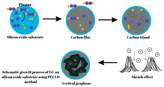
Figure 1. A schematic growth process of VG on a silicon oxide substrate using the PECVD method.
A layer of either amorphous carbon (a-C) or carbide is commonly created in the nucleation stage and is known as a buffer layer [11][12]. The amorphous carbon layer comes from the contrast in the lattice parameters between the graphite and the substrate material. When carbon atoms react with or dissolve into the substrate, this triggers the formation of a carbide layer [10]. Within the structure, a flat or layered graphitic structure can be observed nestled between the amorphous carbon buffer coating and the perpendicular graphene nanosheets. Surrounding the growth of graphene nanosheets is a protective buffer layer that nullifies any substrate-dependent features that could interfere with uniform morphology. Removal of this buffer layer, achievable through etching techniques such as H or OH radicals, benefits the growth of VG nanosheets [13]. Even though vertically grown graphene (VG) nanosheets have a consistent morphology, the reasons behind this are due to three main factors: electric field, internal stress, and anisotropic growth impacts. The creation of the buffer layer and nucleation sites support the VG nanosheet’s unique vertical direction, which distinguishes it from other film formations, such as multi-walled CNTs or MWCNTs.
Hiramatsu [14] proposed a theoretical model of the VG mechanism of growth using the PECVD method, and it is based on five steps:
- (1)
-
The formation of a very thin amorphous carbon layer induced by hydrocarbon radicals (CH4) adsorbed on the substrate followed by ion irradiation to form dangling bonds on the growing surface, resulting in the creation of nucleation sites;
- (2)
-
The formation of nano-islands with dangling bonds due to the migration of adsorbed carbon species on the surface;
- (3)
-
The adsorption of CHx radicals on the surface enhanced by ion irradiation;
- (4)
-
The formation process involves the nucleation of small and disordered nanosheets of graphene at the location of these dangling bonds. This is then accompanied by two-dimensional expansion, which results in the creation of nano-graphene sheets with a haphazard orientation;
- (5)
-
When considering nucleated graphene sheets with varying orientations, those that are nearly vertical to the substrate are more likely to grow faster into vertically standing nanosheets, owing to the electromagnetic fields that are produced by the plasma.
When the growth process is prolonged, the vertical nanowalls that are growing will intersect, leading to the formation of interconnected nanowalls similar to a labyrinth. As the growth period continues, the space between the top of these nanowalls gradually increases, leveling out at a certain point and forming two-dimensional graphenic sheets standing vertically on a substrate, with a high aspect ratio known as vertical graphene (VG) [14]. Figure 2 presents the working principle of the PECVD process.
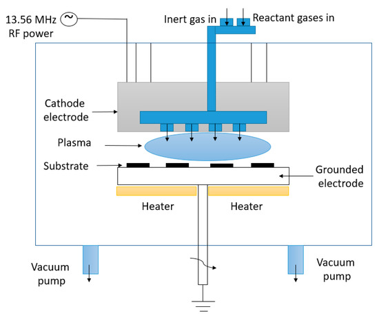
Figure 2. Working principle of the PECVD process.
3. Microwave Plasma-Enhanced Chemical Vapor Deposition (MPECVD) Method
MPECVD was the first method employed to synthesize VG and is also commonly used to generate diamonds and carbon nanotubes. There are three kinds of microwave plasma—TE (transverse electric) Mode, TM (transverse magnetic) Mode, and ECR (electron cyclotron resonance) Mode—based on the microwave’s propagation characteristics. In the TE Mode, the electric field runs at a right angle to the propagation direction. As a result, the charged particles move in a direction that is perpendicular to the substrate plane. When operating in TM Mode, the magnetic field and direction of propagation are at right angles to one another, while the electric field runs parallel. This causes the electrons and ionized carbon radicals to move within the surface plane of the substrate in a microwave time scale. In the presence of ECR, the characteristics of electron transport transform into tensors and functions that hinge on the static magnetic flux intensity. This leads to a three-component vector motion of electrons and ionized carbon radicals [15][16][17].
Wu et al. [15] used the MPECVD method to grow carbon nanowalls. This system has a vertical quartz tube in a microwave cavity with a 500 W microwave source. The gases used are mixtures of CH4 and H2. An important parameter affecting carbon nanostructure growth is the H2/CH4 flow rate ratio. The researchers tested the growth of carbon nanowalls at different H2/CH4 flow rate ratios. They found that any growth with an H2/CH4 flow rate ratio > 50 for 5 min is difficult to obtain. When they reduced this ratio to 30, some amorphous carbon was formed. After many tests, they found that pure carbon nanowalls were received when the gas flow rate ratio was 4–8. The carbon nanowalls grew very fast and had a height of approximately 2 µm, and the width of the nanowall was in the range of 0.1–2 µm.
In 2005, Tanaka et al. [18] reported the growth of VG on a SiO2 substrate by microwave plasma-enhanced chemical vapor deposition. The researchers examined the propagation of the vertical grating (VG) over a SiO2 substrate and discovered that it did not need a catalyst, unlike the procedure of Wu et al. [15]. Furthermore, the investigators observed that the height of VG increased according to the square-root law as it was developed in time; high growth speeds of approximately 10 μm per hour were accomplished. In addition, they found that a valuable gas blend comprising hydrocarbons and hydrogen was employed.
4. Inductively Coupled Plasma-Enhanced Chemical Vapor Deposition (ICP-PECVD) Method
Scientists can generate inductively coupled plasma (ICP) through RF magnetic fields created by the water- or air-cooled copper coils. This mode is suitable for numerous carbon sources, and the frequency is usually between the tens of kHz to the tens of MHz. The most popular frequency used in industrial and research settings is 13.56 MHz RF. For ICP mode, ionized carbon radicals have the same direction as the current in the coil. This kind of plasma generation usually has two approaches, namely, planar ICP and tube/cylinder ICP, and each has its structure. In common practice, both planar inductively coupled plasma (ICP) and tube/cylinder ICP involves the movement of ionized carbon radicals parallel to the substrate plane [19]. Researchers have gradually devised new techniques for synthesizing VG, employing various carbon sources and variant growth strategies. For example, Seo [20] described a synthesis procedure that utilizes honey as the solid carbon source, a combination of argon and hydrogen as the buffer gas, and ICP-PECVD as both the growing system and heating source for the substrate.
Zhu et al. [21] grew carbon nanosheets using the RF-ICP-PECVD method. They used CH4 as a carbon source with a concentration of 40% in the H2 atmosphere. The process parameters for the growth of carbon nanosheets were as follows: pressure of 90 mTorr and RF power of 900 W at a temperature of 680 °C. This group obtained free-standing carbon nanosheets with thicknesses less than 1 nm without any catalyst or special substrate treatment. They could grow carbon nanosheets on different substrates such as Si, SiO2, W, Mo, Cr, Ta, Ti, and many others. Another research group reported the growth of carbon nanowalls using RF-ICP-PECVD and a mixture of CH4 and Ar. Hishikawa et al. [22] obtained carbon nanowalls with a relatively smooth surface using the following process parameters: pressure of 10–60 mTorr, temperature of 700–850 °C, RF power of 500 W, and flow rates of CH4:Ar at 7:1.4 sscm. In 2017, Cuxart et al. [23] used the ICP-PECVD technique to grow VG. They reported several advantages of this method: (a) during the catalyst-free growth of graphene nanosheets, the electric fields from the plasma were minimized; (b) it obtained VG with low defect density; (c) the growth temperature was reduced; and (d) the gas dissociation process was decoupled to allow better deposition of the graphene nanosheets on the substrate. Thus, it is considered that this method allows better control over the growth parameters and precursor gas, leading to better control over the shape and size of the nanostructures.
5. Capacitively Coupled Plasma-Enhanced Chemical Vapor Deposition (CCP-PECVD) Method
The development of capacitively coupled plasma (CCP) involves energizing one capacitor plate through RF power or DC voltage while the other plate remains either grounded or unconnected. Integrating CCP with different types of plasma, such as ICP and surface wave sustained plasma (SWP), creates VG, which leads to increased growth rates but also increases procedure complexity. Moreover, researchers have noted that CCP stimulates ionized carbon radicals to move perpendicular to the substrate plane in experimental settings [24][25].
In 2005, Shiji et al. [25] announced the successful creation of VGs, also known as carbon nanowalls (CNWs). These were made using CCP-PECVD, a process that uses fluorocarbon/hydrogen mixtures and radio-frequency plasma to deposit the material on the desired substrate. An investigation was conducted to assess the correlation between the expansion of VG and the conditions of its production, specifically, the diverse gaseous sources of carbon. Additionally, the study analyzed the impact of plasma’s hydrogen-atom density on VG’s expansion process by employing vacuum ultraviolet absorption spectroscopy.
Compared with ICP, CCP, with its parallel-plane geometry, has a more straightforward setup and can operate at higher pressures. However, its relatively low electron density and energy typically make it an insufficient plasma source to grow high-quality VG sheets. In fact, Langmuir probe measurements have found the plasma density and electron temperature of CCP to be approximately 109–1010 cm−3 and 1011 cm−3 for high-frequency CCP, respectively—much lower compared to other high-density plasma sources such as MW and ICP, which can reach densities from 1010 to 1012 cm−3 and 1013 cm−3, respectively [26][27]. Additionally, the high sheath potentials of CCP can damage surface bonds and further hinder the quality of crystals cultivated. Contamination from electrodes is also a potential issue. Therefore, incorporating a nanostructured catalyst was essential for the successful growth of VG when using CCP as an independent plasma source in a combination of an expanding RF plasma and magnetron sputtering setup. This setup allowed the electron density to reach levels of 1011 cm−3. This is the only successful application of CCP in this context [28][29].
6. Atmospheric-Pressure High Voltage-Enhanced Chemical Vapor Deposition (AHV-PECVD) Method
AHV-PECVD also causes the carbon radicals to move perpendicularly to the substrate surface, though it is typically challenging to grow VG on a large substrate [30]. Bo et al. [30] conducted a rapid synthesis of VG using AHV-PECVD. This research thoroughly outlines a unique reactor structure to manufacture VG sheets in a steady, homogenous production set up by the atmospheric pressure of the PECVD process. Furthermore, they explain the particular experiment executed with a U-shaped reactor design, which entails “dynamic mode” growth (as the metallic substrate is switched between rotational and axial motion during production) and shows the facets it has in comparison to the “static mode” reactor, which keeps the substrate in a fixed position.
7. Electron Beam Excited Plasma-Enhanced Chemical Vapor Deposition (EBEP-PECVD) Method
The EBEP-PECVD system is a unique fusion of DC discharge and electron extraction/acceleration methods, which facilitates the creation of plasma. The LaB6 disk cathode plays a crucial role in sustaining the DC discharge plasma by extracting electrons and propelling them towards the EBEP zone via a set of multi-hole grids. Unlike other synthesis methods, such as magnetron sputtering, TCVD, and HWCVD, the ionized carbon radicals produced here move mainly perpendicular to the substrate under the influence of the applied electric field. Furthermore, this plasma density is related to the pressure of the atmospheric environment and is consequently much higher than that of lower-pressure systems in a vacuum system [16][31].
Other studies for methods of growing VG include Guo et al.’s [32] discovery of a furnace that generates ionized carbon radicals for VG growth by thermally dividing CH4 at temperatures between 800 and 900 °C, also referred to as thermal chemical vapor deposition (TCVD), and Zheng et al.’s [33] explanation of a thermal decomposition procedure utilizing a 1600 °C SiC substrate for VG development. Additionally, there are other techniques, such as magnetron sputtering and thermal hot wire chemical vapor deposition (HWCVD), that have been described. It is important to note that the production of VG is influenced by two crucial plasma parameters: the movement of charged particles and the density of the plasma.
References
- Sun, J.; Rattanasawatesun, T.; Tang, P.; Bi, Z.; Pandit, S.; Lam, L.; Wasén, C.; Erlandsson, M.; Bokarewa, M.; Dong, J.; et al. Insights into the Mechanism for Vertical Graphene Growth by Plasma-Enhanced Chemical Vapor Deposition. ACS Appl. Mater. Interfaces 2022, 14, 7152–7160.
- Shi, L.; Pang, C.; Chen, S.; Wang, M.; Wang, K.; Tan, Z.; Gao, P.; Ren, J.; Huang, Y.; Peng, H.; et al. Vertical Graphene Growth on SiO Microparticles for Stable Lithium Ion Battery Anodes. Nano Lett. 2017, 17, 3681–3687.
- Yazdi, G.R.; Iakimov, T.; Yakimova, R. Epitaxial Graphene on SiC: A Review of Growth and Characterization. Crystals 2016, 6, 53.
- Yuan, S.L.; Gao, G.; Yang, L.; Chhowalla, J.; Gharahcheshmeh, M.H.; Gleason, M.; Choi, K.; Hong, Y.; Liu, B. Chemical vapor deposition. Nat. Rev. Methods Prim. 2021, 1, 5.
- Abbas, Q.; Shinde, P.A.; Abdelkareem, M.A.; Alami, A.H.; Mirzaeian, M.; Yadav, A.; Olabi, A.G. Graphene Synthesis Techniques and Environmental Applications. Materials 2022, 15, 7804.
- Chen, J.; Bo, Z.; Lu, G. Vertically-Oriented Graphene; Springer International Publishing: Cham, Switzerland, 2015; ISBN 978-3-319-15302-5.
- Ghosh, S.; Ganesan, K.; Polaki, S.R.; Mathews, T.; Dhara, S.; Kamruddin, M.; Tyagi, A.K. Influence of substrate on nucleation and growth of vertical graphene nanosheets. Appl. Surf. Sci. 2015, 349, 576–581.
- Muñoz, R.; Gómez-Aleixandre, C.J. Fast and non-catalytic growth of transparent and conductive graphene-like carbon films on glass at low temperature. Phys. D Appl. Phys. 2014, 47, 045305.
- Bo, Z.; Mao, S.; Jun Han, Z.; Cen, K.; Chen, J.; Ostrikov, K. Emerging energy and environmental applications of vertically-oriented graphenes. Chem. Soc. Rev. 2015, 44, 2108–2212.
- Malesevic, A.; Vitchev, R.; Schouteden, K.; Volodin, A.; Zhang, L.; Van Tendeloo, G.; Vanhulsel, A.; Van Haesendonck, C. Synthesis of few-layer graphene via microwave plasma-enhanced chemical vapor deposition. Nanotechnology 2008, 19, 305604.
- Davami, K.; Shaygan, M.; Kheirabi, N.; Zhao, J.; Kovalenko, D.A.; Rummeli, M.H.; Opitz, J.; Cuniberti, G.; Lee, J.-S.; Meyyappan, M. Synthesis and characterization of carbon nanowalls on different substrates by radio frequency plasma enhanced chemical vapor deposition. Carbon 2014, 72, 372–380.
- Cai, M.; Outlaw, R.A.; Butler, S.M.; Miller, J.R. A high density of vertically oriented graphenes for use in electric double layer capacitors. Carbon 2012, 50, 5481–5488.
- Bo, Z.; Yu, K.; Lu, G.; Wang, P.; Mao, S.; Chen, J. Understanding growth of carbon nanowalls at atmospheric pressure using normal glow discharge plasma-enhanced chemical vapor deposition. Carbon 2011, 49, 1849–1858.
- Hiramatsu, M.; Kondo, H.; Hori, M. Graphene Nanowalls Ch.9. In New Progress on Graphene Research; InTech: Rijeka, Croatia, 2013; ISBN 978-953-51-1091-0.
- Wu, Y.H.; Yu, T.; Shen, Z.X. Two-dimensional Carbon Nanostructures: Fundamental Properties, Synthesis, Characterization, and Potential Applications. J. Appl. Phys. 2010, 108, 071301.
- Chuang, A.T.H.; Boskovic, B.O.; Robertson, J. Freestanding Carbon Nanowalls by Microwave Plasma-enhanced Chemical Vapour Deposition. Diam. Relat. Mater. 2006, 15, 1103–1106.
- Thomas, R.; Rao, G.M. Synthesis of 3-dimensional Porous Graphene Nanosheets Using Electron Cyclotron Resonance Plasma Enhanced Chemical Vapour Deposition. RSC Adv. 2015, 5, 84927–84935.
- Tanaka, K.; Yoshimura, M.; Okamoto, A.; Ueda, K. Growth of carbon nanowalls on a SiO2 substrate by microwave plasma-enhanced chemical vapor deposition. Jpn. J. Appl. Phys. 2005, 44, 2074–2076.
- Wang, J.J.; Zhu, M.Y.; Outlaw, R.A.; Zhao, X.; Manos, D.M.; Holloway, B.C. Synthesis of Carbon Nanosheets by Inductively Coupled Radio-frequency Plasma Enhanced Chemical Vapor Deposition. Carbon 2004, 42, 2867–2872.
- Seo, D.H.; Rider, A.E.; Kumar, S.; Randeniya, L.K.; Ostrikov, K. Vertical Graphene Gas- and Bio-sensor Via Catalyst-free, Reactive Plasma Reforming of Natural Honey. Carbon 2013, 60, 221.
- Zhu, M.; Wang, J.; Outlaw, R.A.; Hou, K.; Manos, D.M.; Holloway, B.C. Synthesis of carbon nanosheets and carbon nanotubes by radio frequency plasma enhanced chemical vapor deposition. Diam. Relat. Mater. 2007, 16, 196–201.
- Hishikawa, T.; Hiramatsu, M.; Hori, M. Growth of carbon nanowalls using inductively coupled plasma-enhanced chemical vapor deposition. In Proceedings of the 29th International Symposium on Dry Process, Tokyo, Japan, 13–14 November 2007; pp. 253–254.
- Cuxart, M.G.; Šics, I.; Goñi, A.R.; Pach, E.; Sauthier, G.; Paradinas, M.; Foerster, M.; Aballe, L.; Fernandez, H.M.; Carlino, V.; et al. Inductively coupled remote plasma-enhanced chemical vapor deposition (rPE-CVD) as a versatile route for the deposition of graphene micro- and nanostructures. Carbon 2017, 117, 331–342.
- Kondo, S.; Hori, M.; Yamakawa, K.; Den, S.; Kano, H.; Hiramatsu, M. Highly Reliable Growth Process of Carbon Nanowalls Using Radical Injection Plasma-enhanced Chemical Vapor Deposition. J. Vac. Sci. Technol. B 2008, 26, 1294.
- Shiji, K.; Hiramatsu, M.; Enomoto, A.; Nakamura, M.; Amano, H.; Hori, M. Vertical Growth of Carbon Nanowalls Using RF Plasma Enhanced Chemical Vapor Deposition. Diam. Relat. Mater. 2005, 14, 831.dik.
- Chabert, P.; Braithwaite, N. Physics of Radio-Frequency Plasmas; Cambridge University Press: New York, NY, USA, 2001; pp. 1–385.
- Lieberman, M.A.; Lichtenberg, A.J. Principles of Plasma Discharges and Materials Processing, 2nd ed.; Wiley: Hoboken, NJ, USA, 2005; pp. 1–757.
- Vizireanu, S.; Stoica, S.D.; Luculescu, C.; Nistor, L.C.; Mitu, B.; Dinescu, G. Plasma techniques for nanostructured carbon materials synthesis. A case study: Carbon nanowall growth by low pressure expanding RF plasma. Plasma Sources Sci. Technol. 2010, 19, 034016.
- Malesevic, A.; Vizireanu, S.; Kemps, R.; Vanhulsel, A.; Van Haesendonck, C.; Dinescu, G. Combined growth of carbon nanotubes and carbon nanowalls by plasma-enhanced chemical vapor deposition. Carbon 2007, 45, 2932–2937.
- Bo, Z.; Cui, S.M.; Yu, K.H.; Lu, G.H.; Mao, S.; Chen, J.H. Note: Continuous Synthesis of Uniform Vertical Graphene on Cylindrical Surfaces. Rev. Sci. Instrum. 2011, 82, 086116.
- Mori, T.; Hiramatsu, M.; Yamakawa, K.; Takeda, K.; Hori, M. Fabrication of Carbon Nanowalls Using Electron Beam Excited Plasma-enhanced Chemical Vapor Deposition. Diam. Relat. Mater. 2008, 17, 1513–1517.
- Guo, X.; Quin, S.C.; Bai, S.; Yue, H.W.; Li, Y.L.; Chen, Q.; Li, J.S.; He, D.Y. Vertical Graphene Nanosheets Synthesized by Thermal Chemical Vapor Deposition and the Field Emission Properties. J. Phys. D Appl. Phys. 2016, 49, 385301.
- Zheng, S.H.; Li, Z.L.; Wu, Z.S.; Dong, Y.F.; Zhou, F.; Wang, S.; Fu, Q.; Sun, C.L.; Guo, L.W.; Bao, S.H. High Packing Density Unidirectional Arrays of Vertically Aligned Graphene with Enhanced Areal Capacitance for High Power Micro-Supercapacitors. ACS Nano 2017, 11, 4009.
More
Information
Subjects:
Chemistry, Analytical
Contributors
MDPI registered users' name will be linked to their SciProfiles pages. To register with us, please refer to https://encyclopedia.pub/register
:
View Times:
1.3K
Revisions:
2 times
(View History)
Update Date:
04 May 2023
Table of Contents


Notice
You are not a member of the advisory board for this topic. If you want to update advisory board member profile, please contact office@encyclopedia.pub.
OK
Confirm
Only members of the Encyclopedia advisory board for this topic are allowed to note entries. Would you like to become an advisory board member of the Encyclopedia?
Yes
No
${ textCharacter }/${ maxCharacter }
Submit
Cancel
Back
Comments
${ item }
|
${ item.createdUser.fullName }
${ item.createdAt }
${ item.vote }
${ item.reply }
Delete
${ reply.createdUser.fullName }
${ reply.createdAt }
${ reply.vote }
Delete
There is no reply to this comment~
${ item.replyTextCharacter }/${ item.replyMaxCharacter }
Submit
Cancel
More
No more~
There is no comment~
${ textCharacter }/${ maxCharacter }
Submit
Cancel
${ selectedItem.replyTextCharacter }/${ selectedItem.replyMaxCharacter }
Submit
Cancel
Confirm
Are you sure to Delete?
Yes
No