Your browser does not fully support modern features. Please upgrade for a smoother experience.
Submitted Successfully!
 +1 credit
Thank you for your contribution! You can also upload a video entry or images related to this topic.
For video creation, please contact our Academic Video Service.
| Version | Summary | Created by | Modification | Content Size | Created at | Operation |
|---|---|---|---|---|---|---|
| 1 | Gian-Franco Dalla Betta | -- | 1080 | 2023-04-21 16:09:25 | | | |
| 2 | Camila Xu | Meta information modification | 1080 | 2023-04-23 09:46:37 | | | | |
| 3 | Camila Xu | Meta information modification | 1080 | 2023-04-24 08:28:34 | | |
Video Upload Options
We provide professional Academic Video Service to translate complex research into visually appealing presentations. Would you like to try it?
Cite
If you have any further questions, please contact Encyclopedia Editorial Office.
Dalla Betta, G.; Ye, J.X. Silicon Radiation Detectors: Basic Principles and Requirements. Encyclopedia. Available online: https://encyclopedia.pub/entry/43329 (accessed on 25 July 2026).
Dalla Betta G, Ye JX. Silicon Radiation Detectors: Basic Principles and Requirements. Encyclopedia. Available at: https://encyclopedia.pub/entry/43329. Accessed July 25, 2026.
Dalla Betta, Gian-Franco, Ji Xing Ye. "Silicon Radiation Detectors: Basic Principles and Requirements" Encyclopedia, https://encyclopedia.pub/entry/43329 (accessed July 25, 2026).
Dalla Betta, G., & Ye, J.X. (2023, April 21). Silicon Radiation Detectors: Basic Principles and Requirements. In Encyclopedia. https://encyclopedia.pub/entry/43329
Dalla Betta, Gian-Franco and Ji Xing Ye. "Silicon Radiation Detectors: Basic Principles and Requirements." Encyclopedia. Web. 21 April, 2023.
Copy Citation
Silicon radiation detectors are a special type of microelectronic sensor which plays a crucial role in many applications, from industry to medicine, from cultural heritage to environmental monitoring, homeland security and safety (e.g., in nuclear power plants), to cite but a few, as well as in many fields of fundamental and applied research, including high energy physics (HEP), photon science and astronomy. In this entry, the basic principles and requirements are described, with emphasis on technological aspects.
silicon radiation detectors
fabrication technology
planar detectors
3D detectors
1. Introduction
Radiation detectors are nowadays pervasive in several applications, from industry to medicine, from cultural heritage to environmental monitoring, homeland security and safety (e.g., in nuclear power plants), to cite but a few, as well as in many fields of fundamental and applied research, including high energy physics (HEP), photon science and astronomy.
Starting from the earliest devices, the detection of radiation has been based on different physical mechanisms, such as thermal transduction, gas ionization, scintillation, etc.[1]. As with most other sensor technologies, semiconductors also play a special role in radiation detection for two main reasons: (i) they can directly convert radiation into an electrical signal, ready to be processed by an electronic circuit, and (ii) they are fabricated by exploiting integrated circuit technologies, leading to several advantages, such as small size, low cost as well as improved performance and reliability[2]. Its physical properties (e.g., atomic number, density, ionization energy, bandgap, etc.) make silicon particularly suited for the detection of soft X-rays and charged particles, whereas it is not efficient for hard X-rays/γ-rays and for neutrons (for the detection of which silicon should be coupled with suitable converting materials)[1]. However, silicon is the most widely used semiconductor for detector applications, thanks to the unparalleled advantages of its fabrication technology.
Although silicon detectors are relatively simple devices, they require custom fabrication technologies to optimize their electrical and functional characteristics. Only recently, following the significant progress in CMOS image sensors, pixel detectors made with CMOS technologies (the so-called Monolithic Active Pixels) have proved to yield satisfactory performance[3]. In the future, there will likely be a greater utilization of CMOS pixels, particularly in X-ray imaging and charged particle tracking. However, custom-made detectors are still expected to remain the primary choice for most applications. The market for silicon detectors is considered a specialized one within the field of microelectronics, with only one major industrial manufacturer, Hamamatsu Photonics K.K. of Japan, operating in this area. The majority of the processing facilities are owned by small to medium-sized enterprises (SMEs) and research centers, primarily located in Europe.
2. Basic Principles and Requirements
The most important types of silicon detectors are based on reverse biased p-n junctions[2]. The operation principle is sketched in Figure 1. When traversing through a silicon detector, an impinging radiation creates electron–hole pairs along its path. In the presence of an electric field, these charge carriers are separated and start drifting toward the electrodes, thus inducing a current signal[4], which is fed to an external amplifier.
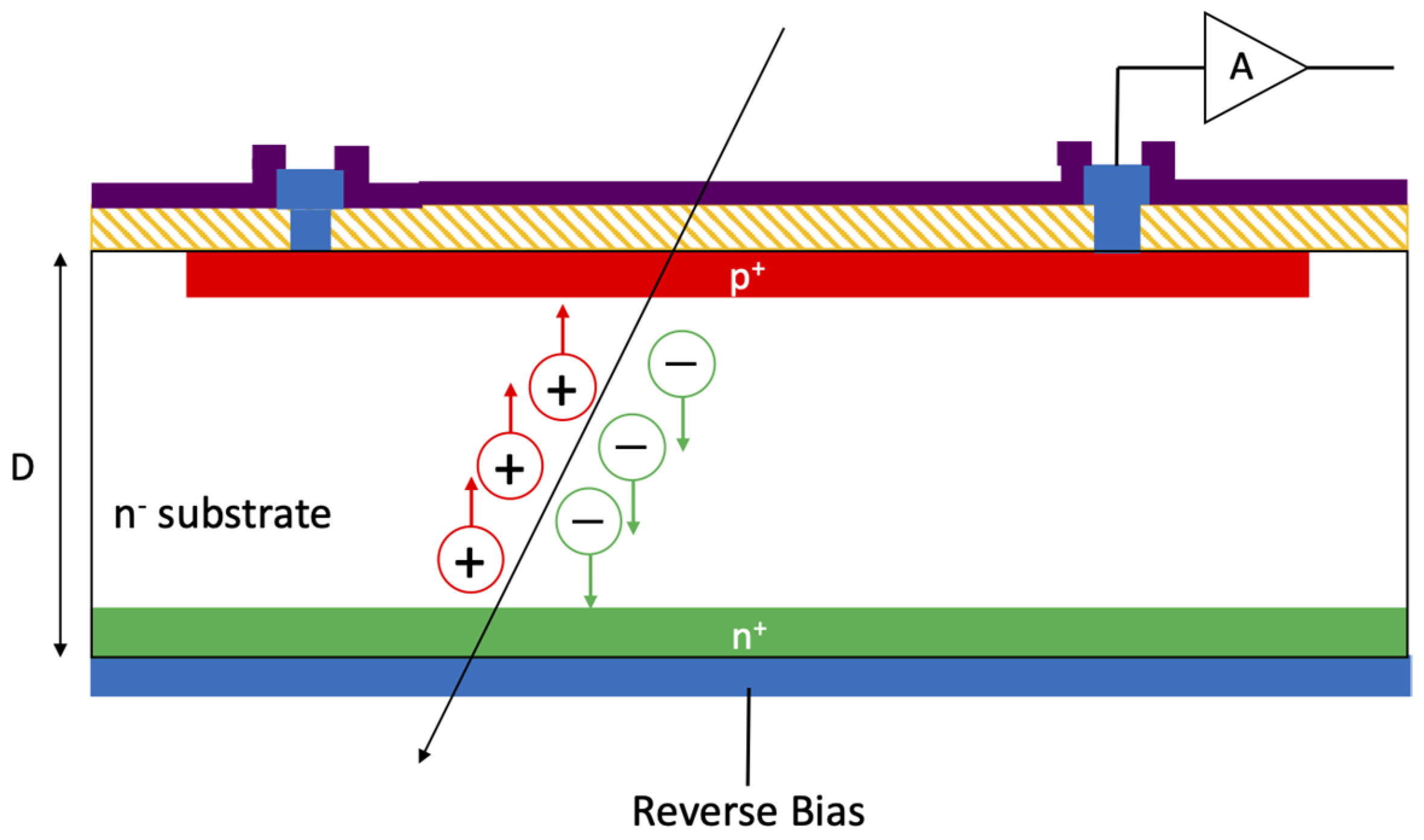
Figure 1. Operation principle of a silicon radiation detector.
Silicon detectors are typically operated in full depletion conditions in order to obtain optimal efficiency, high signal-to-noise ratio and short time response. With reference to the basic theory of an abrupt p+-n junction, the depletion width (w) can be expressed as in Equation (1):
where εSi is the permittivity of silicon, ψ0 the built-in voltage, Vbias the applied reverse bias voltage, q the elementary charge and ND the substrate doping concentration. Thus, the full depletion voltage can be calculated as in Equation (2):
where D is substrate thickness and assuming ψ0 to be negligible. Depending on the applications, D can vary from just a few μm (e.g., for dosimetry) up to ~1 mm (e.g., for X-ray imaging), with the most typical values being of a few hundreds of micrometers. In order to limit the value of full depletion voltage, so as to avoid junction breakdown and reduce power dissipation, the substrate doping concentration should be very low (~1012/cm3).
Despite their simple structure, silicon detectors have some special requirements:
-
Very low leakage currents. Besides affecting power dissipation, the leakage current plays a critical role in the detector noise, so it should be minimized. A value < 1 nA/cm2 is normally assumed as a target. The leakage current is mainly caused by thermal generation in the depleted bulk, so the carrier lifetimes should be high enough, calling for high-purity material and ultra-clean processing, as well as for an optimized layout, often including guard rings[5].
-
Large breakdown voltage. In certain cases, detectors require extremely high voltage to operate effectively. This may be due to factors such as thick substrates, the necessity to achieve high electric fields for velocity saturation, or radiation damage. Specifications often require the breakdown voltage to exceed several hundreds of volts. The use of guard rings is also useful in this respect[6].
-
Radiation hardness. This is especially the case of detectors used in HEP experiments at particle colliders, where the fluences can be as large as ~1016 1-MeV equivalent neutrons per square cm (neq/cm2). Displacement damage to the silicon lattice is here the main issue, with three main consequences[7]: (i) increase in leakage current (linear with fluence); (ii) change in the effective space-charge concentration, leading to an increase in depletion voltage at large fluences; (iii) charge carrier trapping, which represents the factor ultimately limiting the detector performance at fluences beyond~1015 neq/cm2. In addition, ionization damage effects[8] are caused by charged particles but also by high-energy photons (X- and γ-rays), with total ionizing doses that can largely exceed 1 Grad in applications at particle colliders and at Free Electron Laser facilities [9]. The consequences are the build-up of positive charge in the oxides and of interface states, which affect the isolation between n+ regions, the parasitic capacitance between adjacent regions (with impact on noise), the electric fields at the surface (with impact on breakdown voltage) and surface generation/recombination (with impact on leakage current and charge collection in case radiation is absorbed near the surface).
-
Fabrication yield. In silicon detectors, the minimum feature sizes are not too small (~micrometers). Proximity lithography is mainly used, sometimes with double-side alignment. The overall device dimensions can be very large (up to tens of square centimeters) and the specifications often require the total number of defects to be very small, so that yield is certainly a major concern in detector fabrication.
References
- Zhang, J.; Fretwurst, E.; Klanner, R.; Pintilie, I.; Schwandt, J.; Turcato, M. Investigation of X-ray induced radiation damage at the Si-SiO2 interface of silicon sensors for the European XFEL. J. Instrum. 2012, 7, C12012.
- Lutz, G.. Semiconductor Radiation Detectors - Device Physics; Springer: Berlin/Heidelberg, Germany, 2007; pp. 79-107.
- Marco-Hernández, R. Overview of CMOS sensors for future tracking detectors. Instruments 2020, 4, 36.
- Da Rold, M.; Bacchetta, N.; Bisello, D.; Paccagnella, A.; Dalla Betta, G.F.; Verzellesi, G.; Verdini, P.G. Study of breakdown effects in silicon multiguard structures. IEEE Transactions on Nuclear Science 1999, 46, 1215-1223.
- Moll, M. Displacement Damage in Silicon Detectors for High Energy Physics. IEEE Transactions on Nuclear Science 2018, 65, 1561-1582.
- Ma, T,.P.; Dressendorfer, P.V.. Ionizing Radiation Effects in MOS Devices and Circuits; Wiley: New York, NY, USA, 1989; pp. 1-608.
- Moll, M. Displacement Damage in Silicon Detectors for High Energy Physics. IEEE Transactions on Nuclear Science 2018, 65, 1561-1582.
- Ma, T,.P.; Dressendorfer, P.V.. Ionizing Radiation Effects in MOS Devices and Circuits; Wiley: New York, NY, USA, 1989; pp. 1-608.
More
Information
Subjects:
Engineering, Electrical & Electronic
Contributors
MDPI registered users' name will be linked to their SciProfiles pages. To register with us, please refer to https://encyclopedia.pub/register
:
View Times:
1.1K
Revisions:
3 times
(View History)
Update Date:
24 Apr 2023
Table of Contents


Notice
You are not a member of the advisory board for this topic. If you want to update advisory board member profile, please contact office@encyclopedia.pub.
OK
Confirm
Only members of the Encyclopedia advisory board for this topic are allowed to note entries. Would you like to become an advisory board member of the Encyclopedia?
Yes
No
${ textCharacter }/${ maxCharacter }
Submit
Cancel
Back
Comments
${ item }
|
${ item.createdUser.fullName }
${ item.createdAt }
${ item.vote }
${ item.reply }
Delete
${ reply.createdUser.fullName }
${ reply.createdAt }
${ reply.vote }
Delete
There is no reply to this comment~
${ item.replyTextCharacter }/${ item.replyMaxCharacter }
Submit
Cancel
More
No more~
There is no comment~
${ textCharacter }/${ maxCharacter }
Submit
Cancel
${ selectedItem.replyTextCharacter }/${ selectedItem.replyMaxCharacter }
Submit
Cancel
Confirm
Are you sure to Delete?
Yes
No