Your browser does not fully support modern features. Please upgrade for a smoother experience.
Submitted Successfully!
 +1 credit
Thank you for your contribution! You can also upload a video entry or images related to this topic.
For video creation, please contact our Academic Video Service.
| Version | Summary | Created by | Modification | Content Size | Created at | Operation |
|---|---|---|---|---|---|---|
| 1 | Hasan Shabbir | -- | 5196 | 2023-04-04 19:39:05 | | | |
| 2 | Camila Xu | Meta information modification | 5196 | 2023-04-06 02:52:31 | | |
Video Upload Options
We provide professional Academic Video Service to translate complex research into visually appealing presentations. Would you like to try it?
Cite
If you have any further questions, please contact Encyclopedia Editorial Office.
Shabbir, H.; Wojnicki, M. Quantum Dots for Optoelectronic Applications. Encyclopedia. Available online: https://encyclopedia.pub/entry/42798 (accessed on 25 June 2026).
Shabbir H, Wojnicki M. Quantum Dots for Optoelectronic Applications. Encyclopedia. Available at: https://encyclopedia.pub/entry/42798. Accessed June 25, 2026.
Shabbir, Hasan, Marek Wojnicki. "Quantum Dots for Optoelectronic Applications" Encyclopedia, https://encyclopedia.pub/entry/42798 (accessed June 25, 2026).
Shabbir, H., & Wojnicki, M. (2023, April 04). Quantum Dots for Optoelectronic Applications. In Encyclopedia. https://encyclopedia.pub/entry/42798
Shabbir, Hasan and Marek Wojnicki. "Quantum Dots for Optoelectronic Applications." Encyclopedia. Web. 04 April, 2023.
Copy Citation
Quantum dots (QDs) are tiny semiconductor particles that typically range in size from 2 to 10 nanometers. Because of their small size, they have unique optical and electrical properties, resulting in quantum confinement of electrons and holes within the material. This confinement results in discrete energy levels, and the energy of the confined particles is determined by the size of the QDs QDs could be used in a variety of applications, including displays, solar cells, medical imaging, and quantum computing.. They are typically only a few nanometers in size. QDs can be employed as a light-sensitive substance, also referred to as a photoconductive substance, in a photodetector.
quantum dot
confinement
tunable photoexcitation
solar cell
1. Nanomaterials
Nanomaterials have garnered much attention in recent years due to their fascinating and distinctive characteristics that surpass the limitations of bulk materials. Any substance with at least one dimension under 100 nm can be categorized as a nanomaterial [1][2]. Materials with all dimensions larger than nanoscale are called 3D materials or bulk materials, while researchers use a few classifications based on the dimensions of nanomaterials. If two dimensions are larger than the nanoscale, they are called 2D nanomaterials, e.g., quantum wells and nanolayers, a heterostructure composed of two barrier layers sandwiching a single thin well layer. This layer, which contains electrons and holes, is just about 100 Å thick; as a result, the electrons and holes start behaving like waves. In practice, standing waves in a direction perpendicular to the layers correspond to the permissible states in this structure. The system is quantized because only specific waves are standing waves. Many quantum mechanical processes can be observed and controlled in thin quantum well layered semiconductor structures. Modern epitaxial crystal growth techniques can produce them with great precision.
If one dimension of a material is in the nanoscale range and two dimensions are larger than nanoscale, it is categorized as a 1D nanomaterial, e.g., nanorods and nanowires [3][4]. 1D nanomaterials are used in solid-state electronics and as diagnostic tools in medical sciences. They can conduct at the level of one degree of freedom. This enables the utilization of nanowires in applications where electrical conduction is required[5] .
If all dimensions of a material are smaller than 10 nm, it is called a 0D material, e.g., nanoparticles and quantum dots (QDs).
As the size limits approach the zero dimension and the region becomes extremely confined, it is also referred to as a dot. QDs are produced when material sizes become smaller and smaller in each dimension, which causes them to behave like groups of atoms and exhibit fascinating features. The electron–hole pair is also produced by some energy input, such as UV radiation, and the pair is kept together by Coulombic forces [6]. QDs’ size ranges from 2 to 10 nm, or between 10 and 50 atoms, and they have 100 to 1000 electrons. Almost all material systems, including metal, insulators, and semiconductors, exhibit size-dependent electrical or optical characteristics in the quantum size domain. Due to its fundamental and technological significance, the semiconductor’s energy band gap alteration is the most appealing [7]. The materials for the next generation of flat panel displays, photovoltaic, and optoelectronic devices are semiconductors with extensively tunable energy band gaps [8].
Quantum dots (QDs) are tiny semiconductor particles that can be utilized in photodetectors and other applications. They are typically only a few nanometers in size. QDs can be employed as a light-sensitive substance, also referred to as a photoconductive substance, in a photodetector. One example of a photodetector using QDs is a QD infrared photodetector (QDIP) [9][10]. QDIPs use a layer of QDs as the active material, which absorbs the incoming infrared light and generates an electrical current [11]. It has been demonstrated that they have good stability, quick response times, and high sensitivity.
2. Optical and Electrical Properties of Quantum Dots
There are different energies for the electrons in quantum dots. When QDs absorb energy above their band gap, an exciton (electron–hole pair) is created. The electron and hole pair is confined if the diameter of the nanomaterial is smaller than its exciton Bohr radius, often known as the average physical distance between the electron and hole [12]. This electron and hole pair confinement is called the quantum confinement effect, which causes a discrete packet of energy and cannot be considered continuous [13][14]. One of the fascinating phenomena that QDs exhibit is photoluminescence. In this phenomenon, QDs absorb higher-energy photons and release low-energy photons. The electron moves into an excited state upon absorption. When it recombines with a pair, it emits lower energy light. This process takes place in femtoseconds [15].
Photoluminescence generally depends not on the type of materials but on the size [16]. As the quantum dot size decreases, the band gap of the quantum dot increases, causing the emission wavelength to shift toward a lower wavelength, and this is known as the blue shift, which is emission in the visible range. However, the emission can also occur in other regions of the electromagnetic spectrum, such as ultraviolet or infrared. QDs have exciting optical properties such as better photostability, high molar extinction, and high quantum yield (ratio of photons emitted vs. photons absorbed). QDs can be observed using confocal microscopy, fluorescence spectroscopy, total internal reflection microscopy, etc. [17][18].
QDs also have fascinating electrical properties, such as when sufficient energy is absorbed by the QD electron excited from the valence band to the conduction band while leaving the hole (empty state) in the valence band. This hole can be considered a positive mobile charge in the valence band. QDs possess a discrete energy state like an electron of a single atom [19]. Typically, a photon can only form one exciton and excite one electron across the band gap of fluorescent materials, with extra energy being lost as heat. However, multiple exciton generation is possible in QDs, which can be produced simultaneously, increasing the efficiency with which the nanocrystals convert energy [20].
Quantum yield measures the efficiency with which a system converts absorbed light into a different form of energy, such as heat or electricity. In the case of quantum dots, it refers to the efficiency with which the dots convert absorbed light into emitted light [21][22].
The equation for quantum yield is typically expressed as the ratio of the number of photons emitted by the quantum dots to the number of photons absorbed by the dots. This ratio can be expressed as follows:
The quantum yield plays an important role in the properties of QDs. The confinement behaviors produced by QDs’ core/shell structures are closely connected to the core and shell materials [23]. For instance, the electron–hole pair is confined within the core when the energy band gap of the shell material is more significant than that of the core material, and when the energy band gap of core materials is more significant, the electron–hole pair is confined in the shell [24]. QDs, like carbon quantum dots, are extremely sensitive to the presence of extra charges, such as electrons or holes, on their surfaces and in their environment, which can change the photoluminescence and absorption wavelength of QDs. The functional group present on the surface of carbon quantum dots can absorb and trap the photon, which can change the emission wavelength of carbon QDs [25]. Due to these fascinating properties, quantum dots are used in many applications, such as solar cells [26], lasers [27], and photodetectors [28].
3. Quantum Dot Lasers
Semiconductor spherical nanocrystals (colloidal quantum dots), monolayers, and nanowires have found usage in the laser industry. CDs offer wide electromagnetic spectrum emissions from infrared to the visible range due to their size tunability, optical transition, and solution processibility. Compared to conventional semiconductors, QD-based semiconductors are easier to manipulate in size and shape [29]. Due to the unique absorption and emission properties of QDs, it is possible to produce lasing from a single exciton. A QD laser provides even spacing, low threshold amplification, and continuous wave operation. The shell absorbs the energy and acts as an antenna when the core–shell QDs are excited by photons having energies above the energy band gap. These QD outpace Auger recombination, so the threshold for lasing operation decreases [30].
4. Quantum Dots for Solar Cells
For more than two decades, semiconductor quantum dots (QDs) have attracted much attention due to the optoelectronic properties based on zero dimensions. Through the QD band energy level, colloidal quantum dots and self-assembled quantum dots improve the photogeneration of carriers for photovoltaic applications [31]. By expanding the range of photoexcitation, theoretically, it is possible to achieve maximum thermodynamic efficiency although the mechanism of carrier transport and carrier collection also contribute to its efficiency. Self-assembled and colloidal quantum dots are the two most-used types of QDs in solar cell applications [32]. The growth of solar cell wafers is also crucial for their efficiency, including surface passivation and well-controlled heterointerface [33].
Future risks include rising temperatures caused by global warming, shrinking fossil fuel supplies, and ever-increasing energy needs, which will require scientists and researchers to continuously work on developing efficient and affordable renewable energy alternatives [34]. Sunlight, which is abundantly available worldwide and can be converted into electricity or other forms of energy without polluting the environment, is one of the most commonly used renewable energy sources. Photovoltaic systems are based on converting sunlight into electricity, another valuable form of energy [35]. Photovoltaic device usage to produce electrical energy has increased, but obstacles still need to be overcome before these devices can significantly contribute to satisfying the world’s energy needs [36].
Generally, there are three types of solar cells: traditionally, silicon-based monocrystalline and polycrystalline solar cells have been used [37]. The second type is thin-film solar cells, which are less expensive due to the low cost of absorbing material compared to silicon. These include copper gallium indium diselenide, cadmium telluride, and organic solar panels [38]. The third type, perovskite solar cells, uses hybrid organic–inorganic materials as the light-harvesting active layer. Perovskite materials, such as all-inorganic cesium lead halides and methylammonium lead halides, are cheap and straightforward to manufacture. Carrier mobility, doping density, trap density, and diffusion length in films are crucial factors that affect the performance of photovoltaic devices[39] .
Junwei Yang et al. [40]reported synthesizing CdTe core QD-based solar cells. They used the aqueous route to synthesize QDs. CdTe core QDs were first synthesized and then deposited on a TiO2 photoanode. An increase in absorption spectrum is observed for CdTe core QDs compared to CdTe cells. The power conversion efficiency of QD-based solar cells is increased up to 22% compared to CdTe/CdS plain solar cells. The suppressed charge recombination is also confirmed in QD-based solar cells. The authors also reported that thickness plays an important role in quantum efficiency. With optimization of CdSexS1-x shell thickness, about 7.24% conversion efficiency can be achieved, while Jun Du reported that Zn–Cu–In–Se alloyed QDs increase the absorption efficiency when deposited on TiO2 film electrode, and reported conversion efficiency up to 11.66% [41].
5. Nanomaterials for Photodetection
Nanomaterials have properties that are suitable for photodetection, especially two-dimensional nanomaterials Two-dimensional (2D) materials have emerged as promising candidates for photodetectors due to their unique electrical and optical properties. In particular, their ultra-thin structure allows for efficient light absorption and carrier transport, leading to high sensitivity and fast response times. Two examples of 2D materials that are commonly used for photodetectors are:
Graphene is a single layer of carbon atoms arranged in a honeycomb lattice. It has excellent electrical conductivity and high carrier mobility, which makes it an attractive material for photodetectors[42] . When light is absorbed by graphene, it generates electron–hole pairs, which the graphene’s high carrier mobility can efficiently collect. Graphene photodetectors have shown high responsivity and fast response times, making them useful for optical communications and imaging applications, while graphene hybrid composite materials with metallic nanomaterials and inorganic nanomaterials can increase photosensitivity [43].
Transition metal dichalcogenides (TMDs): TMDs are a family of 2D materials consisting of a transition metal atom sandwiched between two chalcogen atoms. They have a direct bandgap, which allows for efficient light absorption and emission [44]. TMDs have shown high sensitivity to light in the visible and near-infrared regions, making them useful for applications such as biomedical imaging and environmental monitoring. In addition, TMDs can be easily integrated with other electronic components, making them promising for on-chip optoelectronics [45]. 2D materials have shown great potential for photodetector applications due to their unique electrical and optical properties. Graphene and TMDs are just two examples of 2D materials that are being actively researched for their photodetection capabilities. As research in this area continues, it is likely that even more promising 2D materials will be discovered and developed for photodetector applications.
Infrared light detection is essential for biological sensing, spectroscopy, and in-depth 3D imaging. At the same time, semiconductors such as silicon, Cds, HgCdTe, and HgS are used for photodetectors. However, these materials have a few drawbacks, such as toxicity, low responsivity, and high cost of fabrication. The imaging performance of the quantum well photodetector, which is comparable to that of the mercury cadmium telluride (HgCdTe) detector, has recently attracted a lot of interest [46].
6. Lead(II) Sulfide (PbS) Quantum Dots
Lead(II) sulfide (PbS) QDs are special semiconductors with distinctive optoelectronic characteristics. Their strong absorption coefficient and band gap of 0.35 eV make them suitable for photovoltaic, photoconductor, and light-emitting diode applications [47][48]. PbS quantum dots are advantageous for sensing and imaging applications because they also have a high quantum yield and a narrow emission spectrum. Furthermore, their band gap can be modified by varying the quantum dot size, enabling further improvement of their optoelectronic characteristics[49][50].
One of these characteristics is their high absorption coefficient, which enables effective light absorption over a broad range of wavelengths. This is because PbS quantum dots have a significant quantum confinement effect, which confines the electrons to a limited area and causes them to have a high absorption coefficient [51].
The high responsivity of PbS quantum dots is a crucial characteristic that makes them effective as photodetectors which means more transformation of absorbed photons into an electrical signal[42][52] . Due to their high electron–hole recombination rate and rapid electron mobility, PbS quantum dots have a high responsiveness that enables the effective conversion of absorbed photons into electrical current. PbS quantum dots are also ideally suited for applications with high sensitivity and low noise because of their excellent signal-to-noise ratio and low dark current[53][54] . Therefore, lead sulfide (PbS) quantum dots (QDs) are considered potential material options for next-generation light, affordable, and flexible photodetectors due to their wide tunable band gaps, high absorption coefficients, and simple solution synthesis methods.
Alberto Maulu et al. synthesized PbS QDs and then modified their surface properties by using 3-mercaptopropionic acid (MPA) and tetrabutylammonium iodide (TBAI)[55] . It was observed that modification with this ligand significantly alters the properties of QDs. MPA-based QDs showed a decrease in dark current and low noise ratio, which causes the enhancement of detective and photosensitivity compared to TBAI-based QDs. MPA-modified QDs have functional group (Pb–OH bonds), while TBAI has a functional group (Pb–I bond), which is the primary reason for the Pb enhancement properties.
QDs used the trap sensitization method to show photoconductivity, increasing the responsivity but decreasing the response time for low optical power. At medium power incidents, light, when traps are filled with both types of photodetector, shows similar types of properties.
Urvashi Bothra et al. investigated the effect of ligands on PbS properties. They showed that a PbX2 [X = I, Br])-based photodetector decreases the trap density compared to a PbS-based device, which increases the performance of (PbS) PbX2-based devices [56].
Jin Beom Kwon et al. fabricated short-wave infrared (SWIR) photodetectors based on PbS QDs [57]. These infrared photodetectors minimize the harmful effect caused by the low wavelength band of SWIR. They fabricated a PbS photodetector with an absorbance peak at 1410 nm and used poly(3-hexylthiophene) (P3HT) as a conductive polymer with PbS QDs. Measurements were made on the properties of the synthesized PbS QDs, and the current–voltage (I–V) features of the PbS SWIR photodetectors. The maximal responsiveness of the PbS SWIR photodetector with P3HT optimization was found to be 2.26 times greater than that of the PbS SWIR photodetector without P3HT. Moreover, the former demonstrated a reduced operating voltage due to the high hole mobility and an adequate highest occupied molecular orbital level of P3HT. Figure 1 shows the I–V characteristics of the PbS-based photodetector.
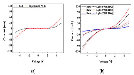
Figure 1. I–V characteristics of (a) PbS SWIR photodetector without P3HT polymer and (b) PbS SWIR photodetector with P3HT polymer[58] .
To compare their performance, they measured the I–V characteristics and responsiveness of the manufactured PbS SWIR photodetectors. The electron–hole pairs produced in the photoactive layer of the PbS SWIR photodetectors were removed from the electrodes by an external electric field when exposed to IR light. When the IR light source was turned off, the dark current was measured, and the light current was measured when the light source was turned on. The output power of the IR light source was 1 W/m2, and the voltage sweep range was between −5 V and 5 V. The highest current difference between the dark current and light current and responsivity was recorded at −5 V in the case of the PbS SWIR photodetector without a P3HT layer. The largest current difference was 23.72 mA, and when this was divided by the input voltage, the corresponding responsivity was calculated as 2635.6 A/W. The PbS SWIR photodetector with a P3HT layer exhibited the best properties when applying 20 mg/mL of P3HT. The greatest current difference was confirmed to be 5891.1 A/W, which is 2.26 times greater than SWIRs, and the maximum current difference was 53.02 mA at −5V.
The drawbacks of current single-layer PbS-QDs photodetectors include excessive dark currents, slow light responses, and poor on–off ratios. It has been demonstrated that combining high-conducting graphene with organic materials and metal nanoparticles to create hybrid PbS-QDs devices can increase photoresponsivity. However, these hybrid devices bring other problems, and Zhenwei Ren et al. [59] synthesized the bilayer QDs device, which can be easily integrated into a flexible polyimide substrate. It increases the responsivity, signal-to-noise ratio, linear dynamic, and detection.
Moreover, this improvement in the device’s properties is attributable to QDs’ significant role. For example, the QDs junction accelerates carrier separation when the light is on. When the light is off, the QDs support the recombination of accumulated carriers in two films via the interface. Junction control is more dominant than trap control, which is the main determining factor in single-layer devices. They fabricated the bilayer photodetector using tetrabutylammonium iodide (TBAI)- and 1,2-ethanedithiol (EDT)-treated QDs. They compared it with a single-layer detector and observed that the bilayer photodetector enhanced optoelectronic properties. The bilayer PbS- TBAI/PbS-EDT devices have higher light current and detection efficiency, while the responsivity of PbS- TBAI/PbS-EDT is comparable to PbS-EDT devices due to the very close photocurrent.
It can be concluded that surface functional chemistry and modification of PbS with ligands improve the performance, and hybrid structure with modifications from different ligands can also improve the performance.
7. Indium Arsenide (InAs) Quantum Dots
Indium arsenide (InAs) quantum dots (QDs) are also potential materials for photodetector sensors due to their distinct optical and electrical characteristics. These QDs are especially beneficial for NIR photodetectors due to their high near-infrared (NIR) absorption coefficient [60]. NIR imaging is one possible use for InAs QD-based photodetectors. Due to InAs QDs’ band gap, developing highly sensitive NIR imaging systems with them is possible. These gadgets are used in telecommunications for sensing, night vision, and medical imaging [61]. Deep-tissue imaging, optical communication, and covert illumination are just a few of the optoelectronics and biomedical uses for indium arsenide quantum dots, which typically emit in the near-infrared spectrum. Systems with bigger optical band gaps have yet to be produced, despite theory suggesting that further quantum confinement through size reduction could enable visible light emission.
NIR spectroscopy is another use for InAs QD-based photodetectors. Due to the NIR light detection capability, highly sensitive NIR spectroscopy devices can be made [62]. Additionally, the development of optoelectronic devices such as solar cells, LEDs, and lasers has utilized InAs QD-based photodetectors. These devices can increase the efficiency of solar cells and other optoelectronic devices by effectively converting light into electrical energy. Applications for these devices include bio-photonics, environmental monitoring, and chemical sensing [63][64] .
Overall, because of their distinct optical and electrical characteristics, as well as their capacity to detect NIR light, InAs QDs have the potential to be utilized in a variety of photodetector applications. They might find use in spectroscopy, optoelectronic devices, and NIR imaging [65]. InAs quantum dots (QDs) might have a different band gap depending on their size and shape. Due to quantum confinement, the band gap of InAs QDs is typically between 0.35 and 0.4 eV, which is lower than that of bulk InAs (0.36 eV) [66].
8. Organic Materials Based on Quantum Dots
Organic materials, such as polymers or small organic compounds, are used to create organic quantum dots (OQDs), a particular kind of quantum dot. Due to their special optical and electronic characteristics, they could be used in photodetector sensors. Organic photovoltaics is one potential use for OQD-based photodetectors (OPVs) [67][68]. The active layer in OPVs, which transform light into electrical energy, can be made of OQDs. OQDs may absorb various wavelengths, which can enhance the efficiency of OPVs. They could also be used to make solar cells that are less expensive than ordinary inorganic solar cells. OQD-based photodetectors can also be used in flexible and wearable gadgets. OQDs offer thin, bendable, and solution-processable advantages, making them ideal for application in bendable and flexible products such as flexible screens and wearable technology [69].
Devices for sensing and bioimaging have also been created using OQDs. OQDs have the potential to be used in biosensing and biomedical imaging, as well as optical imaging. They are advantageous in these applications because of their high quantum yield, strong stability, and great sensitivity[70] . OQDs are a promising material for photodetector sensors overall because of their distinct optical and electronic characteristics and their potential for usage in a variety of applications, including solar cells, flexible and wearable devices, and bio-imaging and sensing equipment [71].
9. Carbon-Based Materials for Photodetection
Carbon materials, such as carbon nanotubes, graphene, and fullerenes, are used to synthesize carbon-based quantum dots (CQDs), a particular kind of quantum dot. Due to their extraordinary optical and electronic characteristics, they could be used in photodetector sensors[72] .
The photodetection of diverse wavelength ranges is one potential use for CQD-based photodetectors. It has been demonstrated that carbon-based quantum dots have a broad absorption spectrum, making them appropriate for use in photodetectors that must detect a variety of wavelengths[73] . They are, therefore, very beneficial for multi-spectral imaging and sensing. High-speed optoelectronics is a further possible use for CQD-based photodetectors. Because of their rapid response times, carbon-based quantum dots can be used in high-speed optoelectronic systems, including optical communications and high-speed data transfer[74] . Devices enabling sensing and bioimaging have also been made with CQDs. The unique optical and electrical characteristics of carbon-based quantum dots make them suitable for biosensing and bioimaging applications, including in vivo imaging. They are helpful in various applications due to their high quantum yield, outstanding stability, and great sensitivity [75]. CQDs are a promising material for photodetector sensors overall because of their distinctive optical and electronic properties and their potential to be employed in a variety of applications, including multi-spectral imaging and sensing, high-speed optoelectronics, and bio-imaging and sensing devices [76].
Both graphene quantum dots (GQD) and carbon dots (CD) are being studied for potential application in photodetector sensors. Small, carbon-based nanoparticles known as CDs have been shown to exhibit robust fluorescence characteristics [77]. On the other hand, GQDs, which are small graphene flakes, have been discovered recently to have fluorescence characteristics similar to those of CDs, with the added advantage of being more stable and simpler to functionalize. CDs and GQDs are promising candidates for photodetector sensors due to their efficiency at absorbing light and transforming it into an electrical signal [78].CDs’ performance is negatively influenced by their inefficient near-infrared (NIR-I and NIR-II) excitation and emission. By resolving this, CDs can be utilized for in vivo bioimaging.
10. Graphene Quantum Dots (GQDs)
There may be applications for graphene quantum dots (GQDs), tiny graphene sheets, in photodetector sensors. Their unique electrical and optical features make them suitable for sensing technologies. GQDs have been found to possess strong fluorescence properties, effectively absorbing light and turning it into an electrical signal [79]. GQDs are extremely stable and may be functionalized with various chemical groups, enabling precise control over their optical and electrical characteristics. They are beneficial for sensing applications requiring specificity and sensitivity[80] .
Graphene, in particular, is a 2D monolayer of sp2 hybrid carbon. At the Dirac point, graphene’s conduction band meets with its valence band. This causes a linear dispersion relationship, making it a zero-band gap semiconductor with zero density of electronic states and an incredibly high room temperature carrier mobility [81]. The broad spectrum response and quick response of graphene are perfect photoelectric qualities due to its zero-band gap semiconducting nature. Although graphene quantum dots have lesser absorption and responsiveness, researchers are primarily focusing on hybridizing graphene with high-absorption materials to enhance photodetection capability like quantum dots [82].
GQDs are also ideally suited for photodetectors and other optoelectronic devices due to their outstanding charge transfer characteristics. Different photodetector designs, including p–n junction, Schottky, and photoconductive ones, can incorporate GQDs [83]. They are helpful for various sensing applications because they can detect a wide range of wavelengths, from visible to infrared.
Molahalli Vandana et al. fabricated a UV-based photodetector by utilizing graphene QDs with polypyrrole polymer [84] . They used two different amounts of graphene, 20 and 40 mL in polypyrrole, labeled as PGC2 and PGC4, while single graphene QDs (GQDs) were also utilized. The active layer of ITO electrode was illuminated with UV light of 265 and 355 nm for about 200 s. The graphene QDs are an excellent light absorber and electron donor to increase the carrier concentration.
11. Carbon Dots
Carbon QDs are nanomaterials made of carbon, similar to substances such as nanodiamonds, fullerenes, carbon nanotubes, graphene, and graphene oxide. Small, water-soluble carbon nanoparticles known as carbon dots (CDs) have been shown to have potential uses in photodetector sensors [85]. CDs are a desirable material for use in sensing technologies due to their distinctive electrical and optical characteristics. Strong fluorescence qualities have been discovered in them, making them efficient at absorbing light and transforming it into an electrical signal [86]. CDs’ high quantum yield and outstanding stability have been found to make them appropriate for use in photodetectors [87]. The precise control of their optical and electrical properties is made possible by their simplicity in synthesis and functionalization. As a result, they are advantageous for sensing applications that demand specificity and sensitivity [88]. CDs’ superior charge transport characteristics have also been discovered, making them suitable for photodetectors and other optoelectronic devices. Many photodetector designs, including p–n junction, Schottky, and photoconductive ones, can incorporate CDs[89] . They are helpful for various sensing applications because they can detect a wide range of wavelengths, from visible to infrared. Additionally, CDs are non-toxic and biocompatible, which makes them advantageous in medicinal applications such as cancer therapy and bioimaging. Additionally, CDs can be functionalized with different biomolecules to enable the detection of certain biomolecules and biological activities [90].
They have gained attention due to their environmentally friendliness, chemical stability, and good conductivity, making them useful in various fields such as biomedical and biotechnological research, solar cells, light-emitting devices, imaging, electrochemical studies, and electrochemiluminescence studies[91] . Carbon dots are a class of nanoparticles composed mainly of carbon and oxygen, while some amino and carboxyl functional groups are also present on the surface[92] . These nanodots have unique optical, electrical, and chemical properties that make them highly versatile and helpful in various applications. Some of the critical properties of carbon dots include: Size: Carbon dots are nanoparticles with diameters ranging from 1 to 10 nanometers. Their small size allows them to display unique properties and quantum confinement effects, which are helpful for a number of applications. These properties make carbon dots valuable for various applications, including sensors, catalysts, and energy storage and conversion. Luminescence: Carbon dots can emit light, making them useful for applications such as biosensors and imaging [93]. Chemical stability: Carbon dots are highly stable in many different chemical environments, including basic and acidic conditions. Their stability makes them useful for sensing and imaging applications. Conductivity: Since CDs have excellent electrical conductivity, carbon dots can be used in photovoltaic and energy storage applications [94]. Biocompatibility: Due to their non-toxicity and biocompatibility, carbon dots can be used in biological systems without damaging healthy cells. Surface functionalization: The surface of carbon dots can be modified with different chemical groups, enabling them to be useful for specific purposes [95]. Optical properties: Carbon dots can absorb light in the ultraviolet and near-infrared parts of the spectrum, making them useful for specific applications. For example, their strong absorbance in these spectrum regions can be utilized in solar cells to absorb and convert sunlight into electricity and in LED lighting to provide energy-efficient and long-lasting light sources [96]. CDs can emit light when excited by an external energy source, such as electricity or heat. The emission wavelength, or the specific range of wavelengths that the light emitted by CDs falls within, can be manipulated by changing the size and composition of the CDs. This can be achieved by using different starting materials or synthesis methods while synthesizing CDs. Solubility: Since they are highly soluble in a wide range of solvents, including water, carbon dots are simple to handle and incorporate into different systems [97]. High surface area: The small size of carbon dots results in a high surface area, which makes them ideal for applications such as catalysis and drug delivery [98].
One crucial property of CDs is their ability to emit light when excited by light, also known as photoluminescence. The photophysical responses of CDs, including their light absorption and emission, are influenced by the isolated network of sp2 carbon bonds in their structure[98] . In contrast, extended networks of carbon bonds, as found in carbon nanotubes, graphite, and graphene, do not interact with light as strongly. This may be due to the rapid recombination of photogenerated electrons and holes without the emission of radiation. CDs typically absorb light over a broad range of wavelengths [99]. They can absorb light over a wide range of wavelengths, but the specific wavelength at which they emit light is determined by the population of a particular energy level or “domain” and the surface properties of the quantum dots. This phenomenon, known as excitation-dependent emission, is a characteristic of CDs arising from these nanomaterials’ surface state. Essentially, the surface of the quantum dots plays a crucial role in determining the specific wavelength at which they will emit light when excited by an external energy source [100].
Carbon dots have a high absorption coefficient, which implies they can absorb a lot of light, in addition to their fluorescence and quenching qualities. Due to their ability to transform light into energy that may be utilized to treat a range of medical problems, they are valuable in phototherapy applications [101].
References
- Ghenadii Korotcenkov Current Trends in Nanomaterials for Metal Oxide-Based Conductometric Gas Sensors: Advantages and Limitations. Part 1: 1D and 2D Nanostructures. Nanomaterials MDPI 2020, 10, 11, https://doi.org/10.1016/j.ijhydene.2020.09.101.
- Chingis Daulbayev , Fail Sultanov , Baglan Bakbolat, Olzhas Daulbayev 0D, 1D and 2D nanomaterials for visible photoelectrochemical water splitting. A Review. International Journal of Hydrogen Energy 2020, 45, 33325-33342, https://doi.org/10.1016/j.ijhydene.2020.09.101.
- Liang Fang,Jing Jing Feng,Xiaobin Shi,Tingzhi Si,Yun Song,Hong Jia,Yongtao Li,Hai-Wen Li,Qingan Zhang Turning bulk materials into 0D, 1D and 2D metallic nanomaterials by selective aqueous corrosion. Chemical Communications 2019, 55, , 10476-10479, https://doi.org/10.1039/C9CC04807C.
- Tingqiang Yang,Yueli Liu,Huide Wang, Yanhong Duo,Bin Zhang, Yanqi Ge,Han Zhang and Wen Chen Recent advances in 0D nanostructure-functionalized low-dimensional nanomaterials for chemiresistive gas sensors. Journal of Materials Chemistry C 2020, 8, 7272-7299, DOI https://doi.org/10.1039/D0TC00387E.
- Erik Garnett, Liqiang Mai, and Peidong Yang Introduction: 1D Nanomaterials/Nanowires. Chemical Reviews 2019, 15, 8955–8957, https://doi.org/10.1021/acs.chemrev.9b00423.
- A.J Nozik Quantum dot solar cells. Physica E: Low-dimensional Systems and Nanostructures 2002, 14, 115-120, https://doi.org/10.1016/S1386-9477(02)00374-0.
- Athanasios B. Bourlinos, Andreas Stassinopoulos, Demetrios Anglos, Radek Zboril, Michael Karakassides, Emmanuel P. Giannelis Surface Functionalized Carbogenic Quantum Dots. Surface Functionalized Carbogenic Quantum Dots 2008, 4, 455-458, https://doi.org/10.1002/smll.200700578.
- Xiangkai Liu, Yuheng Zhang, Ting Yu, Xvsheng Qiao, Ryan Gresback, Xiaodong Pi, Deren Yang Optimum Quantum Yield of the Light Emission from 2 to 10 nm Hydrosilylated Silicon Quantum Dots. Particle & Particle Systems Characterization 2016, 33, 44-52, https://doi.org/10.1002/ppsc.201500148.
- P. Martyniuk, A. Rogalski Quantum-dot infrared photodetectors: Status and outlook. Progress in Quantum Electronics 2008, 32, 89-120, https://doi.org/10.1016/j.pquantelec.2008.07.001.
- Adrienne D. Stiff-Roberts Quantum-dot infrared photodetectors: a review. Journal of Nanophotonics 2009, 3, 031-607, https://doi.org/10.1117/1.3125802.
- H. C. Liu, M. Gao, J. McCaffrey, Z. R. Wasilewski, and S. Fafard Quantum dot infrared photodetectors. Applied Physics Letters 2001, 78, 79 , https://doi.org/10.1063/1.1337649.
- Si-Yu Li and Lin He Recent progresses of quantum confinement in graphene quantum dots. Frontiers of Physics 2022, 17, 33201, https://doi.org/10.1007/s11467-021-1125-2.
- Toshihide Takagahara and Kyozaburo Takeda Theory of the quantum confinement effect on excitons in quantum dots of indirect-gap materials. PHYSICAL REVIEW B 1992, 46, 1557, https://doi.org/10.1103/PhysRevB.46.15578.
- Frank W. Wise Lead salt quantum dots: the limit of strong quantum confinement. Accounts of Chemical Research 2000, 11, 773–780, https://doi.org/10.1021/ar970220q.
- H. Giessen, U. Woggon, B. Fluegel, G. Mohs, Y. Z. Hu, S. W. Koch, and N. Peyghambarian Femtosecond optical gain in strongly confined quantum dots. Optics Letters 1996, 21, 1043-1045, https://doi.org/10.1364/OL.21.001043.
- Maria J. Ruedas-Rama, Angel Orte,a Elizabeth A. H. Hall,b Jose M. Alvarez-Peza and Eva M. Talavera Quantum dot photoluminescence lifetime-based pH nanosensor. Chemical Communications 2011, 47, 2898-2900, DOI https://doi.org/10.1039/C0CC05252C.
- Keenan J. Mintz,Yiqun Zhou,Roger M. Leblanc Recent development of carbon quantum dots regarding their optical properties, photoluminescence mechanism, and core structure. Nanoscale 2019, 11, 4634-4652, DOI: 10.1039/C8NR10059D.
- Shoujun Zhu, Yubin Song, Xiaohuan Zhao, Jieren Shao, Junhu Zhang & Bai Yang The photoluminescence mechanism in carbon dots (graphene quantum dots, carbon nanodots, and polymer dots): current state and future perspective. Nano research 2015, 8, 355–381, https://doi.org/10.1007/s12274-014-0644-3.
- F. Benyettou , A. Aissat , M. Djebari , J.P. Vilcot Electrical properties of InAsP/Si quantum dot solar cell. International Journal of Hydrogen Energy 2017, 42, 19512-19517, https://doi.org/10.1016/j.ijhydene.2017.06.074.
- Greg Jolley, Lan Fu, Hao Feng Lu, Hark Hoe Tan, Chennupati Jagadish Progress in Photovoltaics. Progress in Photovoltaics 2013, 21, 736-746, https://doi.org/10.1002/pip.2161.
- R Emerson The quantum yield of photosynthesis. Annual Review of Plant Physiology 1985, 9, 1-24, https://doi.org/10.1146/annurev.pp.09.060158.000245.
- G. Weber and F. W. J. Teale Determination of the absolute quantum yield of fluorescent solutions. Transactions of the Faraday Society 1957, 53, 646-655, https://doi.org/10.1039/TF9575300646.
- R. Hamood , M.S. Abd El-sadek and A. Gadalla a Facile synthesis, structural, electrical and dielectric properties of CdSe/CdS core-shell quantum dots. Vacuum 2018, 157, 291-298, https://doi.org/10.1016/j.vacuum.2018.08.050.
- Karen Grieve, Paul Mulvaney, Franz Grieser Synthesis and electronic properties of semiconductor nanoparticles/quantum dots. Current Opinion in Colloid & Interface Science 2000, 168-172, 5, https://doi.org/10.1016/S1359-0294(00)00050-9.
- L P Kouwenhoven, D G Austingand S Tarucha Few-electron quantum dots. Reports on Progress in Physics 2001, 64, 6, 10.1088/0034-4885/64/6/201.
- Jun Du, Zhonglin Du, Jin-Song Hu, Zhenxiao Pan, Qing Shen, Jiankun Sun, Donghui Long, Hui Dong, Litao Sun, Xinhua Zhong, and Li-Jun Wan Zn–Cu–In–Se quantum dot solar cells with a certified power conversion efficiency of 11.6%. Journal of the American Chemical Society 2016, 12, 4201–4209, https://doi.org/10.1021/jacs.6b00615.
- I.P. Marko; A.R. Adams; S.J. Sweeney; D.J. Mowbray; M.S. Skolnick; H.Y. Liu; K.M. Groom Recombination and loss mechanisms in low-threshold InAs-GaAs 1.3-/spl mu/m quantum-dot lasers. IEEE Journal of Selected Topics in Quantum Electronics 2005, 11, 5, DOI: 10.1109/JSTQE.2005.853847.
- Young-Shin Park, Wan Ki Bae, Jeffrey M. Pietryga, and Victor I. Klimov Auger recombination of biexcitons and negative and positive trions in individual quantum dots. ACS Nano 2014, 7, 7288–7296, https://doi.org/10.1021/nn5023473.
- Pieter Geiregat, Dries Van Thourhout and Zeger Hens A bright future for colloidal quantum dot lasers. NPG Asia Materials 2019, 11, 11, NPG Asia Materials.
- I.P. Marko; A.R. Adams; S.J. Sweeney; D.J. Mowbray; M.S. Skolnick; H.Y. Liu; K.M. Groom Recombination and loss mechanisms in low-threshold InAs-GaAs 1.3-/spl mu/m quantum-dot lasers. IEEE Journal of Selected Topics in Quantum Electronics 2005, 11, 1041 - 1047, DOI: 10.1109/JSTQE.2005.853847.
- OCTAVI E. SEMONIN, JOSEPH M. LUTHER, SUKGEUN CHOI, HSIANG-YU CHEN, JIANBO GAO, ARTHUR J. NOZIK , AND MATTHEW C. BEARD Peak external photocurrent quantum efficiency exceeding 100% via MEG in a quantum dot solar cell. Science 2011, 334, 1530-1533, DOI: 10.1126/science.1209845.
- Graham H. Carey, Ahmed L. Abdelhady, Zhijun Ning, Susanna M. Thon∥, Osman M. Bakr and Edward H. Sargent Colloidal quantum dot solar cells. Chemical Reviews 2015, 23, 12732–12763, https://doi.org/10.1021/acs.chemrev.5b00063.
- Prashant V. Kamat Quantum Dot Solar Cells. The Next Big Thing in Photovoltaics. The Journal of Physical Chemistry Letters 2013, 6, 908–918, https://doi.org/10.1021/jz400052e.
- Windmanagda Sawadogo , Babatunde J. Abiodun , Emmanuel C. Okogbue Impacts of global warming on photovoltaic power generation over West Africa. Renewable Energy 2020, 151, 263-277, https://doi.org/10.1016/j.renene.2019.11.032.
- Martin A Green Photovoltaic technology and visions for the future. Progress in Energy 2019, 1, 1, DOI 10.1088/2516-1083/ab0fa8.
- Andreev, V M; Grilikhes, V A; Rumyantsev, V D Photovoltaic conversion of concentrated sunlight. ETDEWEB 1997, 1, 1, Photovoltaic conversion of concentrated sunlight.
- Mohammadreza Aghaei A review on comparison between traditional silicon solar cells and thin-film CdTe solar cells. National Graduate Conference 2012 (NatGrad 2012), Tenaga Nasional Universiti, 2012, 1, 1, A review on comparison between traditional silicon solar cells and thin-film CdTe solar cells.
- Rolf Brendel Review of layer transfer processes for crystalline thin-film silicon solar cells. Japanese Journal of Applied Physics 2001, 40, 7R, DOI 10.1143/JJAP.40.4431.
- YAOGUANG RONG , YUE HU , ANYI MEI , HAIREN TAN , MAKHSUD I. SAIDAMINOV , SANG IL SEOK , MICHAEL D. MCGEHEE , EDWARD H. SARGENT , AND HONGWEI HAN Challenges for commercializing perovskite solar cells. Science 2018, 361, 6408, DOI: 10.1126/science.aat8235.
- Junwei Yanga and Xinhua Zhong CdTe based quantum dot sensitized solar cells with efficiency exceeding 7% fabricated from quantum dots prepared in aqueous media. Journal of Materials Chemistry A 2016, 4, 16553-16561, DOI https://doi.org/10.1039/C6TA07399A.
- Jun Du, Zhonglin Du, Jin-Song Hu, Zhenxiao Pan, Qing Shen, Jiankun Sun, Donghui Long, Hui Dong, Litao Sun, Xinhua Zhong, and Li-Jun Wan Zn–Cu–In–Se quantum dot solar cells with a certified power conversion efficiency of 11.6%. Journal of the American Chemical Society 2016, 12, 4201–4209, https://doi.org/10.1021/jacs.6b00615.
- Bangtong Ge, Changbin Nie and Jun Shen A hybrid photodetector of graphene/TiO2/inorganic PbS quantum dots for fast response. Japanese Journal of Applied Physics 2022, 61, 4, DOI 10.35848/1347-4065/ac56fc.
- Biswajit Kundu, Onur Özdemir, Mariona Dalmases, Gaurav Kumar, Gerasimos Konstantatos Hybrid 2D‐QD MoS2–PbSe Quantum Dot Broadband Photodetectors with High‐Sensitivity and Room‐Temperature Operation at 2.5 µm. Advanced Optical Materials 2021, 9, 21, https://doi.org/10.1002/adom.202101378.
- Antonia Kagkoura, Dr. Theodosis Skaltsas, Dr. Nikos Tagmatarchis Transition‐Metal Chalcogenide/Graphene Ensembles for Light‐Induced Energy Applications. Chemistry: A European Journal 2017, 23, 12967-12979, https://doi.org/10.1002/chem.201700242.
- Komal Jaiswal, Yarabahally R. Girish, and Mrinmoy De Group-VI-Chalcogenide-Based Nanomaterials in Photo/Thermal Organic Transformations. https://doi.org/10.1021/accountsmr.2c00110 2022, 10, 1033–1048, https://doi.org/10.1021/accountsmr.2c00110.
- Abhijit Chatterjee , Naresh Babu Pendyala, Amardeep Jagtap, K. S. R. Koteswara Rao Uncooled mid-wave infrared focal plane array using band gap engineered mercury cadmium telluride quantum dot coated silicon roic. e-Journal of Surface Science and Nanotechnology 2019, 17, 95-100, https://doi.org/10.1380/ejssnt.2019.95.
- P. Hoyer and R. Könenkamp Photoconduction in porous TiO2 sensitized by PbS quantum dots. Applied Physics Letters 1995, 66, 3, https://doi.org/10.1063/1.114209.
- Haibin Wang, Takaya Kubo, Jotaro Nakazaki, and Hiroshi Segawa Solution-processed short-wave infrared PbS colloidal quantum Dot/ZnO nanowire solar cells giving high open-circuit voltage. ACS Energy Letters 2017, 9, 2110–2117, https://doi.org/10.1021/acsenergylett.7b00505.
- Biswajit Kundu, Onur Özdemir, Mariona Dalmases, Gaurav Kumar, Gerasimos Konstantatos Hybrid 2D‐QD MoS2–PbSe Quantum Dot Broadband Photodetectors with High‐Sensitivity and Room‐Temperature Operation at 2.5 µm. Advanced Optical Materials 2021, 9, 22, https://doi.org/10.1002/adom.202101378.
- Jianbo Gao, Craig L. Perkins, Joseph M. Luther, Mark C. Hanna, Hsiang-Yu Chen, Octavi E. Semonin, Arthur J. Nozik, Randy J. Ellingson, and Matthew C. Beard n-Type transition metal oxide as a hole extraction layer in PbS quantum dot solar cells. Nano Letters 2011, 8, 3263–3266.
- Yang Liu, Hao Wu, Guozheng Shi, Yusheng Li, Yiyuan Gao, Shiwen Fang, Haodong Tang, Wei Chen, Tianshu Ma, Irfan Khan, Kai Wang, Changlei Wang, Xiaofeng Li, Qing Shen, Zeke Liu, Wanli Ma Merging Passivation in Synthesis Enabling the Lowest Open‐Circuit Voltage Loss for PbS Quantum Dot Solar Cells. Advanced Materials 2023, 35, 2207293, https://doi.org/10.1002/adma.202207293.
- Chi Zhang, Linyuan Lian, Zhaoliang Yang, Jianbing Zhang, and Haiming Zhu Quantum Confinement-Tunable Ultrafast Charge Transfer in a PbS Quantum Dots/WSe2 0D–2D Hybrid Structure: Transition from the Weak to Strong Coupling Regime. The Journal of Physical Chemistry Letters 2019, 24, 7665–7671, https://doi.org/10.1021/acs.jpclett.9b03293.
- Yuanzhi Wei, Zhenwei Ren, Andong Zhang, Peng Mao, Hui Li, Xinhua Zhong, Weiwei Li, Shiyong Yang and Jizheng Wang Hybrid organic/PbS quantum dot bilayer photodetector with low dark current and high detectivity. Advanced Functional Materials 2018, 28, 1706690, https://doi.org/10.1002/adfm.201706690.
- Dominik Kufer, Ivan Nikitskiy, Tania Lasanta, Gabriele Navickaite, Frank H. L. Koppens and Gerasimos Konstantatos Hybrid 2D–0D MoS2–PbS Quantum Dot Photodetectors. Advanced Materials 2015, 27, 176-180, https://doi.org/10.1002/adma.201402471.
- Alberto Maulu ,Juan Navarro-Arenas ,Pedro J. Rodríguez-Cantó ,Juan F. Sánchez-Royo ,Rafael Abargues ,Isaac Suárez and Juan P. Martínez-Pastor Charge transport in trap-sensitized infrared PbS quantum-dot-based photoconductors: Pros and cons. Nanomaterials 2018, 8, 9, https://doi.org/10.3390/nano8090677.
- Urvashi Bothra, Miguel Albaladejo-Siguan, Yana Vaynzof, Dinesh Kabra Impact of Ligands on the Performance of PbS Quantum Dot Visible–Near‐Infrared Photodetectors. Advanced Optical Materials 2022, 11, 1, https://doi.org/10.1002/adom.202201897.
- Jin Beom Kwon ,Maeum Han ,Dong Geon Jung ,Seong Ho Kong and Daewoong Jung High sensitivity shortwave infrared photodetector based on PbS QDs using P3HT. Nanomaterials 2021, 11, 10, https://doi.org/10.3390/nano11102683.
- Jin Beom Kwon ,Maeum Han ,Dong Geon Jung ,Seong Ho Kong and Daewoong Jung High Sensitivity Shortwave Infrared Photodetector Based on PbS QDs Using P3HT. Nanomaterials 2021, 11, 10, https://doi.org/10.3390/nano11102683.
- Yuanzhi Wei, Zhenwei Ren, Andong Zhang, Peng Mao, Hui Li, Xinhua Zhong, Weiwei Li, Shiyong Yang, Jizheng Wang Hybrid organic/PbS quantum dot bilayer photodetector with low dark current and high detectivity. Advanced Functional Materials 2018, 28, 11, https://doi.org/10.1002/adfm.201706690.
- Daniel Franke, Daniel K. Harris, Ou Chen, Oliver T. Bruns, Jessica A. Carr, Mark W. B. Wilson & Moungi G. Bawendi Continuous injection synthesis of indium arsenide quantum dots emissive in the short-wavelength infrared. Nature Communications 2016, 7, 12749, https://doi.org/10.1038/ncomms12749.
- Uri Banin, YunWei Cao, David Katz & Oded Millo Identification of atomic-like electronic states in indium arsenide nanocrystal quantum dots. Nature 1999, 400, 542–544, https://doi.org/10.1038/22979.
- Sang-Wook Kim, John P. Zimmer, Shunsuke Ohnishi, Joseph B. Tracy, John V. Frangioni, and Moungi G. Bawendi Engineering InAsxP1-x/InP/ZnSe III−V Alloyed Core/Shell Quantum Dots for the Near-Infrared. Journal of the American Chemical Society 2005, 30, 10526–10532, https://doi.org/10.1021/ja0434331.
- Houman Bahmani Jalali , Luca De Trizio , Liberato Manna l and Francesco Di Stasio Indium arsenide quantum dots: an alternative to lead-based infrared emitting nanomaterials. Chemical Society Reviews 2022, 51, 9861-9881, DOI: 10.1039/D2CS00490A .
- Youngrong Park , Sanghwa Jeong , Sungjee Kim Medically translatable quantum dots for biosensing and imaging51-70. Journal of Photochemistry and Photobiology C: Photochemistry Reviews 2017, 30, 51-70, https://doi.org/10.1016/j.jphotochemrev.2017.01.002.
- Y Fu , F Ferdos, M Sadeghi , Q.X Zhao , S.M Wang , A Larsson Strain and optical transitions in InAs quantum dots on (001) GaAs. Superlattices and Microstructures 2011, 30, 205-213, https://doi.org/10.1006/spmi.2001.1009.
- C. Dion, P. Desjardins, N. Shtinkov, M. D. Robertson, F. Schiettekatte, P. J. Poole, and S. Raymond Intermixing during growth of InAs self-assembled quantum dots in InP: A photoluminescence and tight-binding investigation. PHYSICAL REVIEW B 2009, 77, 075338, https://doi.org/10.1103/PhysRevB.77.075338.
- Huu Tuan Nguyen , Raja Das , Anh Tuan Duong , Soonil Lee Influence of quantum dot concentration on the opto-electronic properties of colloidal quantum-dots LEDs. Optical Materials 2020, 109, 110251, https://doi.org/10.1016/j.optmat.2020.110251.
- Teng Wang, Chunyang Nie, Zhimin Ao, Shaobin Wang and Taicheng An Recent progress in gC 3 N 4 quantum dots: synthesis, properties and applications in photocatalytic degradation of organic pollutants. Journal of Materials Chemistry A 2020, 8, 485-502, https://doi.org/10.1039/C9TA11368A.
- Emily A. Weiss Organic molecules as tools to control the growth, surface structure, and redox activity of colloidal quantum dots. Accounts of chemical research 2013, 11, 2607–2615, https://doi.org/10.1021/ar400078u.
- Jingjing Liab and Jun-Jie Zhu Quantum dots for fluorescent biosensing and bio-imaging applications. Analyst 2013, 138, 2506-2515, DOI https://doi.org/10.1039/C3AN36705C.
- Barbara Vercelli The role of carbon quantum dots in organic photovoltaics: a short overview. Coating MDPI 2021, 11, 2, https://doi.org/10.3390/coatings11020232.
- Amirhossein Alaghmandfard , Omid Sedighi , Nima Tabatabaei Rezaei , Amir Abbas Abedini , Adrine Malek Khachatourian , Muhammet S. Toprak , Alexander Seifalian Recent advances in the modification of carbon-based quantum dots for biomedical applications. Materials Science and Engineering: C 2021, 120, 111756, https://doi.org/10.1016/j.msec.2020.111756.
- Pooria Namdari , Babak Negahdari, Ali Eatemadi Synthesis, properties and biomedical applications of carbon-based quantum dots: An updated review. Biomedicine & Pharmacotherapy 2017, 87, https://doi.org/10.1016/j.biopha.2016.12.108, https://doi.org/10.1016/j.biopha.2016.12.108.
- Anli Xu, Gang Wang, Yongqiang Li, Hui Dong, Siwei Yang, Peng He, Guqiao Ding Carbon‐based quantum dots with solid‐state photoluminescent: mechanism, implementation, and application. Small 2020, 16, 2004621, https://doi.org/10.1002/smll.202004621.
- Pengju G. Luo, Fan Yang, Sheng-Tao Yang, Sumit K. Sonkar, Liju Yang, Jessica J. Broglie, Yun Liu and Ya-Ping Sun Carbon-based quantum dots for fluorescence imaging of cells and tissues. RSC Advances 2014, 4, 10791-10807, DOI https://doi.org/10.1039/C3RA47683A.
- Parambath Anilkumar, Xin Wang, Li Cao, Sushant Sahu, Jia-Hui Liu, Ping Wang, Katerina Korch, Kenneth N. Tackett , Alexander Parenzana and Ya-Ping Sun Toward quantitatively fluorescent carbon-based “quantum” dots. Nanoscale 2011, 3, 2023-2027, DOI https://doi.org/10.1039/C0NR00962H.
- Brandon K. Walther , Cerasela Zoica Dinu , Dirk M. Guldi , Vladimir G. Sergeyev , Stephen E. Creager , John P. Cooke and Anthony Guiseppi-Elie Nanobiosensing with graphene and carbon quantum dots: Recent advances. Materials Today 2020, 39, 23-46, https://doi.org/10.1016/j.mattod.2020.04.008.
- Sofia Paulo ,Emilio Palomares and Eugenia Martinez-Ferrero Graphene and carbon quantum dot-based materials in photovoltaic devices: from synthesis to applications. Nanomaterials 2016, 6, 9, https://doi.org/10.3390/nano6090157.
- Mitchell Bacon, Siobhan J. Bradley, Thomas Nann Graphene quantum dots. Particle & Particle Systems Characterization 2014, 31, 415-428, https://doi.org/10.1002/ppsc.201300252.
- P. Tian , L. Tang , K.S. Teng , S.P. Lau Graphene quantum dots from chemistry to applications. Materials today chemistry, 2018, 10, 221-258, https://doi.org/10.1016/j.mtchem.2018.09.007.
- Mao-Kun Zhang, Wei-Di Liu, You-Pin Gong, Qingfeng Liu and Zhi-Gang Chen Graphene/Quantum Dot Heterostructure Photodetectors: From Material to Performance. Advanced Optical Materials 2022, 10, 2201889, https://doi.org/10.1002/adom.202201889.
- Domenico De Fazio, Burkay Uzlu, Iacopo Torre, Carles Monasterio-Balcells, Shuchi Gupta, Tymofiy Khodkov, Yu Bi, Zhenxing Wang, Martin Otto, Max C. Lemme, Stijn Goossens, Daniel Neumaier*, and Frank H. L. Koppens* Graphene–quantum dot hybrid photodetectors with low dark-current readout. ACS Nano 2008, 9, 11897–11905, https://doi.org/10.1021/acsnano.0c04848.
- Gerasimos Konstantatos, Michela Badioli, Louis Gaudreau, Johann Osmond, Maria Bernechea, F. Pelayo Garcia de Arquer, Fabio Gatti & Frank H. L. Koppens Hybrid graphene–quantum dot phototransistors with ultrahigh gain. Nature Nanotechnology 2012, 1, 1, https://doi.org/10.1038/nnano.2012.60.
- Molahalli Vandana ,Hundekal Devendrappa ,Paola De Padova , and Gurumurthy Hegde Polymer Nanocomposite Graphene Quantum Dots for High-Efficiency Ultraviolet Photodetector. Nanomaterials 2022, 12, 18, https://doi.org/10.3390/nano12183175.
- Li Cao, Sheng-Tao Yang, Xin Wang, Pengju G. Luo, Jia-Hui Liu, Sushant Sahu, Yamin Liu, and Ya-Ping Sun✉ Competitive performance of carbon “quantum” dots in optical bioimaging. Theranostics 2012, 3, 295–301, doi: 10.7150/thno.3912.
- Xiaoyu Zhang, Qingsen Zeng, Yuan Xiong, Tianjiao Ji, Chen Wang, Xinyu Shen, Min Lu, Haoran Wang, Shanpeng Wen, Yu Zhang, Xuyong Yang, Xin Ge, Wei Zhang, Aleksandr P. Litvin, Alexander V. Baranov, Dong Yao, Hao Zhang, Bai Yang, Andrey L. Rogach, Weitao Zheng Energy level modification with carbon dot interlayers enables efficient perovskite solar cells and quantum dot based light‐emitting diodes. Advanced Functional Materials 2020, 30, 1910530, https://doi.org/10.1002/adfm.201910530.
- Liming Hu , Yun Sun , Shengliang Li , Xiaoli Wang , Kelei Hu , Lirong Wang , Xing-jie Liang , Yan Wu Multifunctional carbon dots with high quantum yield for imaging and gene delivery. Carbon 2014, 67, 508-513, https://doi.org/10.1016/j.carbon.2013.10.023.
- Mohammed J. Meziani, Xiuli Dong, Lu Zhu, Les P. Jones, Gregory E. LeCroy, Fan Yang, Shengyuan Wang, Ping Wang, Yiping Zhao, Liju Yang, Ralph A. Tripp, and Ya-Ping Sun Visible-light-activated bactericidal functions of carbon “Quantum” dots. ACS Applied Materials & Interfaces 2016, 17, 10761–10766, https://doi.org/10.1021/acsami.6b01765.
- Xiaoxu Chen, Chao Yang, Huijin Sun, Shougui Ning, Hao Zhou, Hong Zhang, Shutong Wang, Guoying Feng and Shouhuan Zhou Enhanced photoresponsivity in carbon quantum dots-coupled graphene/silicon Schottky-junction photodetector. Laser Physics Letters 2019, 1, 1, DOI 10.1088/1612-202X/ab2040.
- Joaquim C.G. Esteves da Silva and Helena M.R. Gonçalves Analytical and bioanalytical applications of carbon dots. TrAC Trends in Analytical Chemistry 2011, 30, 1327-1336, https://doi.org/10.1016/j.trac.2011.04.009.
- Kuan-Wu Chu ,Sher Ling Lee ,Chi-Jung Chang , and Lingyun Liu Recent Progress of Carbon Dot Precursors and Photocatalysis Applications. Polymers MDPI 2019, 11, 4, https://doi.org/10.3390/polym11040689.
- Xiaoyu Zhang, Yu Zhang, Yu Wang, Sergii Kalytchuk, Stephen V. Kershaw, Yinghui Wang, Peng Wang, Tieqiang Zhang, Yi Zhao, Hanzhuang Zhang, Tian Cui, Yiding Wang, Jun Zhao, William W. Yu, and Andrey L. Rogach Color-Switchable Electroluminescence of Carbon Dot Light-Emitting Diodes. ACS Nano 2013, 12, 11234–11241, https://doi.org/10.1021/nn405017q.
- Manju Kurian and Anju Paul Recent trends in the use of green sources for carbon dot synthesis–A short review. Carbon Trends 2021, 3, 100032, https://doi.org/10.1016/j.cartre.2021.100032.
- Ruiting Guo , Lin Li , Baowei Wang , Yinger Xiang , Guoqiang Zou , Yirong Zhu , Hongshuai Hou , Xiaobo Ji Functionalized carbon dots for advanced batteries. Energy Storage Materials 2021, 37, 8-39, https://doi.org/10.1016/j.ensm.2021.01.020.
- Hasan Shabbir ,Tomasz Tokarski ,Ditta Ungor and Marek Wojnicki Eco friendly synthesis of carbon dot by hydrothermal method for metal ions salt identification. Materials 2021, 14, 24, https://doi.org/10.3390/ma14247604.
- Xiangcao Li , Shaojing Zhao , Baoling Li , Ke Yang , Minhuan Lan and Lintao Zeng Advances and perspectives in carbon dot-based fluorescent probes: Mechanism, and application. Coordination Chemistry Reviews 2021, 431, 213686, https://doi.org/10.1016/j.ccr.2020.213686.
- Bibekananda De and Niranjan Karak * A green and facile approach for the synthesis of water soluble fluorescent carbon dots from banana juice. RSC Advances 2023, 3, 8286-8290, DOI: 10.1039/C3RA00088E.
- Bibekananda De and Niranjan Karak A green and facile approach for the synthesis of water soluble fluorescent carbon dots from banana juice. RSC Advances 2013, 3, 8286-8290, DOI: 10.1039/C3RA00088E.
- Nikita V. Tepliakov, Evgeny V. Kundelev, Pavel D. Khavlyuk, Yuan Xiong, Mikhail Yu. Leonov, Weiren Zhu, Alexander V. Baranov, Anatoly V. Fedorov, Andrey L. Rogach, and Ivan D. Rukhlenko sp2–sp3-Hybridized Atomic Domains Determine Optical Features of Carbon Dots. ACS Nano 2019, 9, 10737–10744, https://doi.org/10.1021/acsnano.9b05444.
- Wenquan Shi ,Qiurui Han ,Jiajia Wu ,Chunyu Ji ,Yiqun Zhou ,Shanghao Li ,Lipeng Gao ,Roger M. Leblanc and Zhili Peng Synthesis Mechanisms, Structural Models, and Photothermal Therapy Applications of Top-Down Carbon Dots from Carbon Powder, Graphite, Graphene, and Carbon Nanotubes. International Journal of Molecular Sciences 2022, 23, 3, https://doi.org/10.3390/ijms23031456.
- Wen-Kui Li , Jun-Tao Feng , Zhi-Qing Ma Nitrogen, sulfur, boron and flavonoid moiety co-incorporated carbon dots for sensitive fluorescence detection of pesticides. Carbon 2020, 161, 685-693, https://doi.org/10.1016/j.carbon.2020.01.098.
More
Information
Subjects:
Nanoscience & Nanotechnology
Contributors
MDPI registered users' name will be linked to their SciProfiles pages. To register with us, please refer to https://encyclopedia.pub/register
:
View Times:
1.7K
Revisions:
2 times
(View History)
Update Date:
06 Apr 2023
Table of Contents


Notice
You are not a member of the advisory board for this topic. If you want to update advisory board member profile, please contact office@encyclopedia.pub.
OK
Confirm
Only members of the Encyclopedia advisory board for this topic are allowed to note entries. Would you like to become an advisory board member of the Encyclopedia?
Yes
No
${ textCharacter }/${ maxCharacter }
Submit
Cancel
Back
Comments
${ item }
|
${ item.createdUser.fullName }
${ item.createdAt }
${ item.vote }
${ item.reply }
Delete
${ reply.createdUser.fullName }
${ reply.createdAt }
${ reply.vote }
Delete
There is no reply to this comment~
${ item.replyTextCharacter }/${ item.replyMaxCharacter }
Submit
Cancel
More
No more~
There is no comment~
${ textCharacter }/${ maxCharacter }
Submit
Cancel
${ selectedItem.replyTextCharacter }/${ selectedItem.replyMaxCharacter }
Submit
Cancel
Confirm
Are you sure to Delete?
Yes
No