Your browser does not fully support modern features. Please upgrade for a smoother experience.
Submitted Successfully!
 +1 credit
Thank you for your contribution! You can also upload a video entry or images related to this topic.
For video creation, please contact our Academic Video Service.
| Version | Summary | Created by | Modification | Content Size | Created at | Operation |
|---|---|---|---|---|---|---|
| 1 | Itilekha Podder | -- | 1778 | 2023-03-20 10:29:00 | | | |
| 2 | Sirius Huang | Meta information modification | 1778 | 2023-03-21 01:44:23 | | |
Video Upload Options
We provide professional Academic Video Service to translate complex research into visually appealing presentations. Would you like to try it?
Cite
If you have any further questions, please contact Encyclopedia Editorial Office.
Podder, I.; Fischl, T.; Bub, U. Micro-Electromechanical Systems. Encyclopedia. Available online: https://encyclopedia.pub/entry/42347 (accessed on 16 July 2026).
Podder I, Fischl T, Bub U. Micro-Electromechanical Systems. Encyclopedia. Available at: https://encyclopedia.pub/entry/42347. Accessed July 16, 2026.
Podder, Itilekha, Tamas Fischl, Udo Bub. "Micro-Electromechanical Systems" Encyclopedia, https://encyclopedia.pub/entry/42347 (accessed July 16, 2026).
Podder, I., Fischl, T., & Bub, U. (2023, March 20). Micro-Electromechanical Systems. In Encyclopedia. https://encyclopedia.pub/entry/42347
Podder, Itilekha, et al. "Micro-Electromechanical Systems." Encyclopedia. Web. 20 March, 2023.
Copy Citation
Micro-electromechanical systems (MEMS) technology-based sensors have found diverse fields of application due to the advancement in semiconductor manufacturing technology, which produces sensitive, low-cost, and powerful sensors. Due to the fabrication of different electrical and mechanical components on a single chip and complex process steps, MEMS sensors are prone to deterministic and random errors.
artificial intelligence
machine learning
micro-electromechanical systems
manufacturing process
sensors
1. Introduction
Micro-electromechanical systems (MEMS) devices are rugged, small, and silicon-based and are fabricated in the micrometer range with advanced technologies, such as semiconductor manufacturing. MEMS involves electrical and mechanical components fabricated using Integrated circuits (IC) batch processing at the micrometer scale [1]. Often, multiple devices are fabricated into a single chip, and cross-signal interaction and interference are unavoidable. This is why new failure modes are introduced and must be taken care of efficiently.
Figure 1 depicts a simplified MEMS manufacturing process. After the design, process simulation, layout, and mask generation, the micro-fabrication process starts with a silicon substrate. The material deposition, pattern transfer, and excess material removal run multiple cycles until the desired result is achieved. Compared to traditional IC fabrication techniques, thicker films and deeper etching lead to fewer cycles to achieve the desired result. Special probing and sectioning techniques are used to protect the parts. Testing and calibration are crucial in the MEMS manufacturing process to retain high quality and reliability. The complexity comes from the spatial distribution of the wafers, the process-induced effects, and the combination of both. Moreover, complexity plays such an important role because the useful signal from the MEMS and the degree of fluctuations/effects from the process (temperature, pressure, mechanical stress, gas concentration, etc.) are much more comparable than in the case of a macroscopic product. At the same time, the expectation is that each product has the same properties compared to its specification.
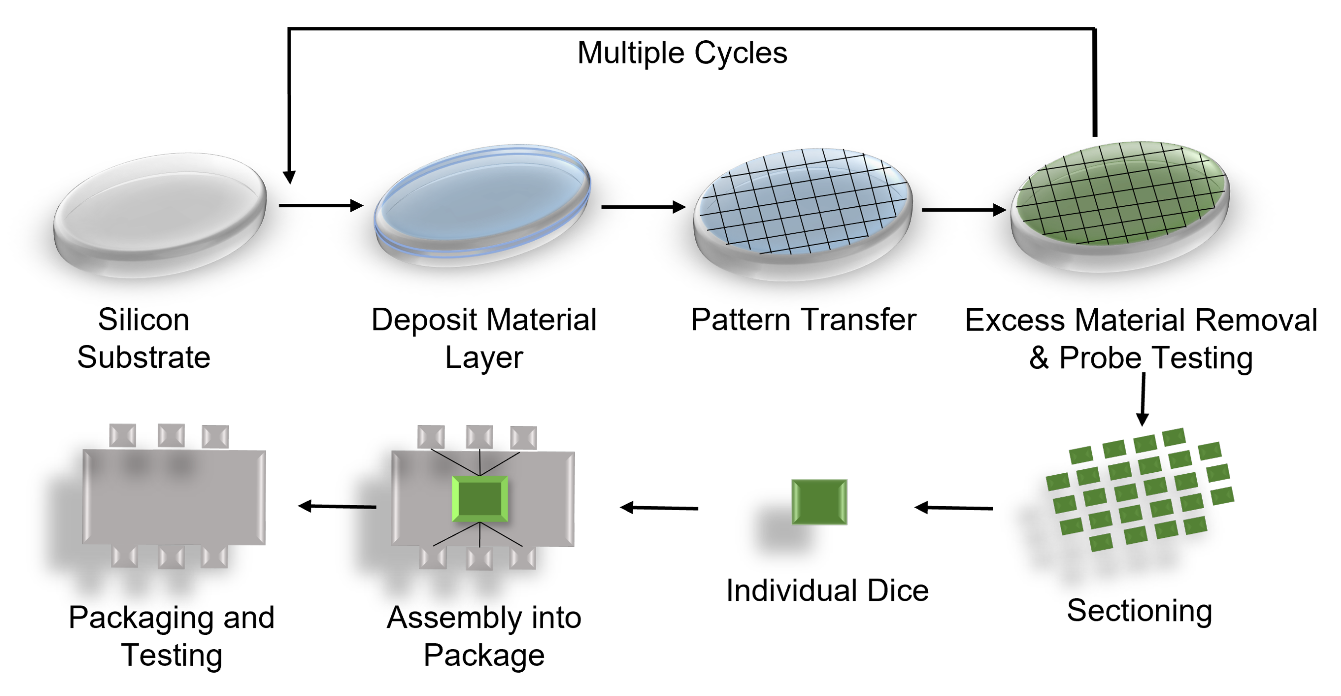
Figure 1. MEMS Manufacturing Process.
In comparison to traditional sensors, MEMS-based sensors provide significant advantages, such as (i) low production cost, (ii) less power consumption, (iii) improved sensing in terms of accuracy and sensitivity, (iv) lightweight, (v) more diminutive size, (vi) high and straightforward integration, (vii) parallelism, (viii) resilient to shock, vibration, and radiation, (xi) scalability, etc. MEMS-based gyroscopes and accelerometers were first developed around the 1990s for automotive applications, triggering the high demand for consumer electronics. Mid-2000 marked the boom of MEMS sensors by incorporating MEMS sensors into Nintendo’s Wii. Later, a high adaptation rate could be seen in other areas, such as smartphones, microphones, motion detection, image stabilization, home security, wearable devices, such as fitness watches, the automotive industry, military, unmanned aerial vehicles (UAV), air crafts, etc. Due to more interest and research in autonomous vehicles, it has become more critical than ever.
MEMS’s current market size value in 2022 is 14.32 billion USD and is projected to reach 75 billion USD by 2032 with a global growth rate of 18.01% from 2022–2032 [2]. Advancements in new technology, such as sensor fusion, big data, AI, and the industrial internet of things, created opportunities for new application areas, such as smart homes, connected cars, and autonomous vehicles.
2. MEMS Components
As can be seen from Figure 2, MEMS are not only sensors; MEMS components can be subdivided into four categories, (1) microelectronics, (2) microactuators, (3) microsensors, and (4) microstructures, which are integrated into a single chip. Microsensors sense the physical parameters and detect changes in stimuli, such as pressure, temperature, motion, mass, light, etc. The microelectronics then process and analyze the collected information, which sends the signal to the microactuators. Upon receiving the signal, the microactuators respond and provide outputs as a change in the environment. MEMS components are packaged together with an application-specific integrated circuit (ASIC), which acts as an electrical interface among the components to send and receive analog and digital information. This makes the calibration and packaging processes quite complicated.
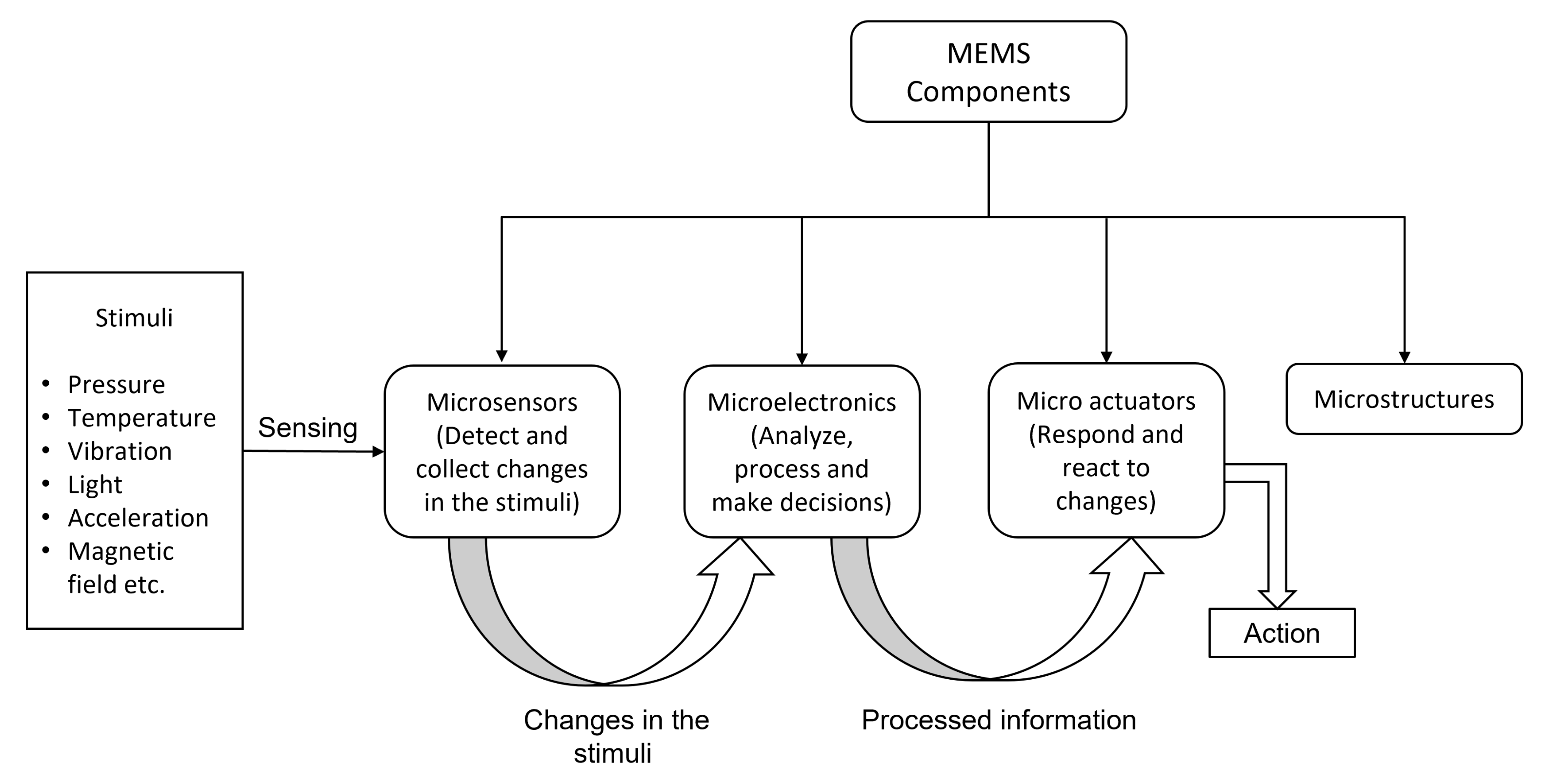
Figure 2. MEMS Components Overview.
Types of MEMS Sensors and Applications
Based on the received responses and measured quantity, the microsensors used in MEMS can be broadly divided into different types, such as physical, chemical, and biological.
Table 1 shows a high-level classification of the microsensors used in MEMS-based systems [3] based on the received signal. MEMS sensors can be classified in many ways, such as application area, adaptation rate, popularity, MEMS structure, etc., but this is not in the scope of this text. The most common form of application and adaptation will be discussed for simplicity.
Table 1. Microsensor Classification.
| Sensor Types | Input Signal Type | Measured quantity |
|---|---|---|
| Physical | Mechanical, Electric, Magnetic, Optical, Thermal, etc. | Acceleration, Force, Pressure, Charge, Magnetic field |
| Chemical | Gas, Humidity, etc. | Toxic gases, Flammable gases, pH, H+, Metallic ions, etc. |
| Biological | Enzyme, Immuno, etc. | Glucose, Lactic acid, Protein, Virus, etc. |
Popular MEMS sensor types according to application:
- Accelerometers
- Gyroscopes
- Pressure sensors
- Temperature sensors
- Inertial Measurement Units (IMU)
- Proximity sensors etc.
Most common MEMS inertial sensors consist of accelerometers and gyroscopes. It will be later seen that the contributions made in MEMS inertial sensors are pretty impressive.
In general, accelerometers can be divided into two categories based on the response type, such as (1) AC-response and (2) DC-response. AC-response accelerometers consist of piezoelectric elements for sensing. Thus, they are also known as piezoelectric accelerometers. The piezoelectric element “displaces” a charge when the accelerometer experiences acceleration, resulting in an electrical output proportional to acceleration. DC-response accelerometers can be of two types: piezoresistive (mainly used for low-range devices) and capacitive (high accuracy and sensitivity). They make use of MEMS fabrication technology, which scales to big-volume applications and lowers the cost of production. The advantages of using a MEMS-based accelerometer over a piezoelectric accelerometer are (i) active self-test, (ii) can measure both dynamic and static movement, (iii) generates precise velocity and displacement information, (iv) excellent bias stability and minimal noise, etc.
The most commonly used MEMS accelerometer is the capacitive type, which is the cheapest and smallest. The accelerometer can be a single-axis, where acceleration is measured or a multi-axis, where the orientation of gravity is measured as well. The accelerometer measures acceleration in terms of movement, shock, or vibration. The basic working principle can be explained with a mass suspended on a spring attached to a fixed frame, i.e., a comb capacitor plate. In the presence of an external force, the mass moves, and the distance between the fixed plate and the seismic mass changes. This further changes the capacitance between the set and the movable plate [4][5]. The challenge of this design is to provide DC accuracy over temperature and reduce the temperature drift and bias drift as much as possible. The drift compensation by AI algorithm has become an attractive research topic. From an application perspective, MEMS accelerometers are used in smartphones, airbags in cars, cameras for anti-blur, real time applications, such as the military, etc.
MEMS vibratory gyroscopes measure the angular rate of rotation or displacement by using Coriolis force. Based on the transduction type, a MEMS gyroscope can be of different types, such as silicon tuning fork, quartz tuning fork, vibratory ring, etc. The purpose of a gyroscope is to measure the acceleration of its oscillating mechanical sensing components. The mechanical structure remains in active resonance, and a small displacement as a response is produced due to Coriolis acceleration [6]. Managing this quadrature signal requires a clever gyroscope design so that the small signal is detectable. This is why many electronic compensation methods exist to de-noise the signal. Thus, noise modeling, random drift construction, temperature drift compensation, fault detection, and diagnosis of the gyroscope have become some of the most lucrative fields of interest for data scientists. The main application areas can be found in stability control in the automotive industry, short-range navigation, such as missile navigation, image stabilization in industrial applications, submarines, UAVs, aeronautics navigation, etc.
3. MEMS Manufacturing Process
The MEMS manufacturing process is an extensive and time-consuming endeavor that requires numerous quality checks before completing the entire process. The design requires simultaneously considering devices from electrical, mechanical, and electronic domains. Not only that, the design should consider the cross-domain effect and analyze it. MEMS fabrication is based on chemical etching and photo-lithography. It consists of bulk micro-machining, surface micro-machining, and high-aspect-ratio micro-machining using techniques, such as LIGA (Lithographie, Galvanoformung, Abformung-Lithography, Electroplating, and Molding) [7]. New micro-manufacturing methods, including micro-mechanical cutting, micro-electrical discharge machining, micro-electrochemical machining, micro-forming, laser technology, laser-assisted forming, replication techniques, deposition methods, etc., have been emerging to create a hybrid process. Multiple companies exist, such as MEMSCAP Inc., IntelliSense Software Corp, ABAQUS, Inc., Coventor Inc., etc., and research bodies, such as U.C. Berkeley, Carnegie Mellon University, TU Chemnitz, etc., who are continuously working on providing improved solutions for MEMS design [8]. Figure 3 shows a high-level overview of the MEMS design structure flow [9][10]. Given the numerous steps involved, several challenges occur at different levels, such as design issues, fabrication issues, bulk micro-machining issues, dicing issues, packaging issues, technical issues [11][12] etc.
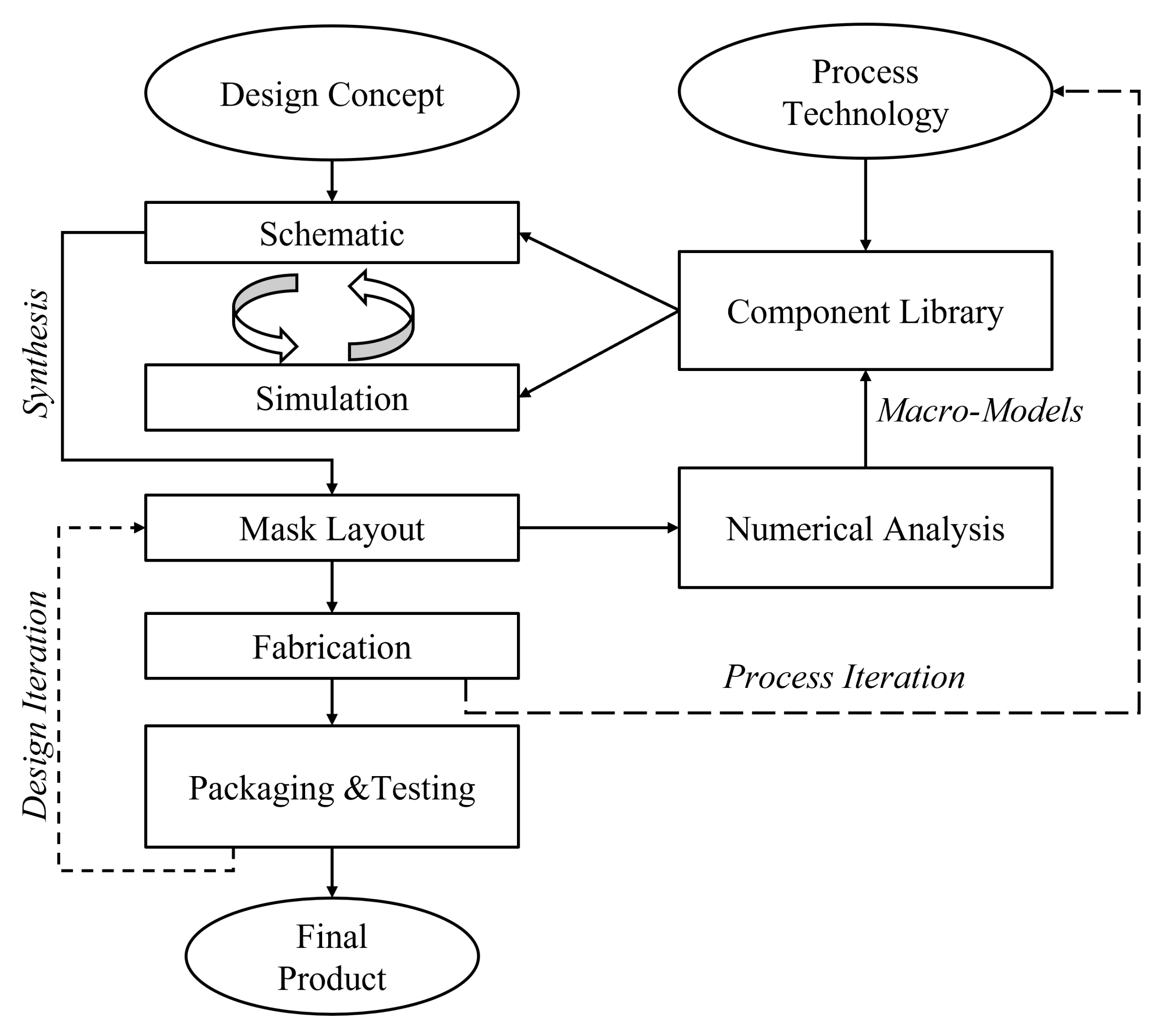
Figure 3. Detailed MEMS Design Flow Schematic Diagram.
As stated in article [13], manufacturing defects can be categorized into the following three categories.
-
Type A defects: These types of defects are evenly random with a stable mean density. There is no repeated occurrence or visible systematic pattern, i.e., the probability of a dice being good or bad is equal. Thus, the root-cause analysis of such defects is not straightforward. Only an accurate and stable process can help reduce these kinds of defects.
-
Type B defects: These types of defects are repeatable and of systematic pattern from wafer to wafer. These defects’ source can be generated from anomalies in the process or machine, such as mask induced or during the variation while applying films.
-
Type C defects: The most common type of defect seen in semiconductor manufacturing is Type C defect, a combination of Type A and Type B defects. It is essential to eliminate random defects to recognize and eradicate systemic flaws. There can be multiple causes, such as structural defects coming from the raw material, asymmetrical presence of contaminants, irregular presence of defect generation particles, etc.
All these defects can be visible or invisible. The visible wafer defects can be classified as local, random, center, and scrape based on the visual pattern type. Currently, manual inspections are performed to detect visible surface anomalies, which are prone to erroneous outcomes.
The lack of a standardized framework to resolve the aforementioned issues obstructs the manufacturing process. However, this can not be achieved easily as the expected solutions are based on the nature and complexity of the problems. The solution requires in-depth domain knowledge and process knowledge and can be cumbersome. Given the rise in the market demand for cheaper, smaller, and high-performance MEMS sensors, organizations and researchers are constantly looking for new means to improve the MEMS sensor production process to meet the market demand. This is where AI can provide a massive benefit for process optimization.
References
- Allen, J.J. Introduction to MEMS (MicroElectroMechanical Systems); Technical Report; Sandia National Lab. (SNL-NM): Albuquerque, NM, USA, 2007.
- MEMS Sensor Market Outlook (2022-2032). Available online: https://www.factmr.com/report/4528/mems-sensor-market (accessed on 18 November 2022).
- Tai, Y.C. Introduction to MEMS. In Microsystems and Nanotechnology; Zhou, Z., Wang, Z., Lin, L., Eds.; Springer: Berlin/Heidelberg, Germany, 2012; pp. 187–206.
- Malayappan, B.; Lakshmi, U.P.; Rao, B.P.; Ramaswamy, K.; Pattnaik, P.K. Sensing Techniques and Interrogation Methods in Optical MEMS Accelerometers: A Review. IEEE Sens. J. 2022, 22, 6232–6246.
- Zhai, Y.; Li, H.; Tao, Z.; Cao, X.; Yang, C.; Che, Z.; Xu, T. Design, fabrication and test of a bulk SiC MEMS accelerometer. Microelectron. Eng. 2022, 260, 111793.
- Passaro, V.M.; Cuccovillo, A.; Vaiani, L.; De Carlo, M.; Campanella, C.E. Gyroscope technology and applications: A review in the industrial perspective. Sensors 2017, 17, 2284.
- Saile, V.; Wallrabe, U.; Tabata, O.; Korvink, J.G. LIGA and Its Applications; Hoboken, NJ, USA, 2009; Volume 7.
- Su, Y.C.; Lin, L. MEMS Design. In Microsystems and Nanotechnology; Zhou, Z., Wang, Z., Lin, L., Eds.; Springer: Berlin/Heidelberg, Germany, 2012; pp. 261–285.
- Fan, Z.; Seo, K.; Hu, J.; Rosenberg, R.C.; Goodman, E.D. System-level synthesis of MEMS via genetic programming and bond graphs. In Proceedings of the Genetic and Evolutionary Computation Conference, Chicago, IL, USA, 12–16 July 2003; pp. 2058–2071.
- Antonsson, E.; Cavallaro, J.; Mcnc, R.; Ann, M.; Intellisense, F. Structured Design Methods for MEMS Final Report; California Inst. Technology: Pasadena, CA, USA, 1997.
- Pattanaik, P.; Ojha, M. Review on challenges in MEMS technology. Mater. Today Proc. 2021.
- Qin, Y.; Brockett, A.; Ma, Y.; Razali, A.; Zhao, J.; Harrison, C.; Pan, W.; Dai, X.; Loziak, D. Micro-manufacturing: Research, technology outcomes and development issues. Int. J. Adv. Manuf. Technol. 2010, 47, 821–837.
- Kaempf, U. The binomial test: A simple tool to identify process problems. IEEE Trans. Semicond. Manuf. 1995, 8, 160–166.
More
Information
Subjects:
Engineering, Manufacturing
Contributors
MDPI registered users' name will be linked to their SciProfiles pages. To register with us, please refer to https://encyclopedia.pub/register
:
View Times:
1.7K
Revisions:
2 times
(View History)
Update Date:
21 Mar 2023
Table of Contents


Notice
You are not a member of the advisory board for this topic. If you want to update advisory board member profile, please contact office@encyclopedia.pub.
OK
Confirm
Only members of the Encyclopedia advisory board for this topic are allowed to note entries. Would you like to become an advisory board member of the Encyclopedia?
Yes
No
${ textCharacter }/${ maxCharacter }
Submit
Cancel
Back
Comments
${ item }
|
${ item.createdUser.fullName }
${ item.createdAt }
${ item.vote }
${ item.reply }
Delete
${ reply.createdUser.fullName }
${ reply.createdAt }
${ reply.vote }
Delete
There is no reply to this comment~
${ item.replyTextCharacter }/${ item.replyMaxCharacter }
Submit
Cancel
More
No more~
There is no comment~
${ textCharacter }/${ maxCharacter }
Submit
Cancel
${ selectedItem.replyTextCharacter }/${ selectedItem.replyMaxCharacter }
Submit
Cancel
Confirm
Are you sure to Delete?
Yes
No