Submitted Successfully!
To reward your contribution, here is a gift for you: A free trial for our video production service.
Thank you for your contribution! You can also upload a video entry or images related to this topic.
Version Summary Created by Modification Content Size Created at Operation
1 -- 2771 2023-03-04 22:59:27 |
2 format correct -2 word(s) 2769 2023-03-06 01:58:04 |

Video Upload Options

Do you have a full video?

Confirm

Are you sure to Delete?
Cite
If you have any further questions, please contact Encyclopedia Editorial Office.
Giacomini, G. LGAD-Based Silicon Sensors for 4D Detectors. Encyclopedia. Available online: https://encyclopedia.pub/entry/41875 (accessed on 27 July 2024).
Giacomini G. LGAD-Based Silicon Sensors for 4D Detectors. Encyclopedia. Available at: https://encyclopedia.pub/entry/41875. Accessed July 27, 2024.
Giacomini, Gabriele. "LGAD-Based Silicon Sensors for 4D Detectors" Encyclopedia, https://encyclopedia.pub/entry/41875 (accessed July 27, 2024).
Giacomini, G. (2023, March 04). LGAD-Based Silicon Sensors for 4D Detectors. In Encyclopedia. https://encyclopedia.pub/entry/41875
Giacomini, Gabriele. "LGAD-Based Silicon Sensors for 4D Detectors." Encyclopedia. Web. 04 March, 2023.
LGAD-Based Silicon Sensors for 4D Detectors
Edit

Low-Gain Avalanche Diodes (LGAD) are a class of silicon sensors developed for the fast detection of Minimum Ionizing Particles (MIPs). The development was motivated by the need of resolving piled-up tracks of charged particles emerging from several vertexes originating from the same bunch-crossing in High-Energy Physics (HEP) collider experiments, which, however, are separated not only in space but also in time by a few tens of picoseconds. Built on thin silicon substrates and featuring an internal moderate gain, they provide fast signals for excellent timing performance, which are therefore useful to distinguish the different tracks. Unfortunately, this comes at the price of poor spatial resolution. To overcome this limitation, other families of LGAD-based silicon sensors which can deliver in the same substrate both excellent timing and spatial information are under development.

LGAD avalanche photodiodes APD silicon sensors

1. LGAD

The basic unit of an LGAD is a p–n junction, where a shallow phosphorus layer is implanted on a thin p-type substrate (Figure 1). The n is implanted at a high dose to have low sheet and contact resistances. It is contacted by a metal layer (usually aluminum as it is typical in all other silicon sensors) and then connected to the read-out electronics by wire (or bump) bonding. As in any silicon sensor where n electrodes are patterned, it is necessary to isolate them from each other because the fixed positive oxide charge induces an electron layer at the oxide/silicon interface which would short-circuit the n pixels. The standard solution, valid also for LGADs, is to introduce a boron layer compensating for the electron accumulation layer between the pixels by either patterning a boron layer surrounding the n-electrodes (p-stop) or by the use of a uniform layer (p-spray) over the entire surface [1].
Figure 1. Sketch, not to scale, of a typical cross section of an LGAD, showing the main components as described in the text.
As they are engineered to detect MIPs traversing the substrate with fast timing, a high electric field which is traversed by electrons is required. In fact, as ionization coefficients in silicon are higher for electrons than for holes (for the same electric field), the gain is due to the multiplication of electrons. High-enough electric fields are created by implanting a deep boron layer a fraction of a micron to a few microns under the n+ phosphorus already implanted at the interface. Upon depletion of the boron layer, a high electric field develops. LGADs do not work in Geiger mode but rather in the linear region. Here, only electrons are multiplied as electric fields are low enough for a significant hole multiplication to occur, preventing the onset of avalanche breakdowns. While the electrons are multiplied and create secondary electrons and holes, these secondary holes, which drift back towards the p+ contact, are responsible for the majority of the signal, according to Ramo’s theorem [2].
These active layers are necessary to achieve fast timing, as the signal must develop in a very short time (order of one nanosecond). Typically, 20–50 μm thick substrates are used for LGADs. A standard clean-room (but the same applies to CMOS foundries) cannot process such thin substrates unless they are placed on a thick carrier wafer (order of a few hundreds of microns thick). Initial substrates are of two possible kinds: a thin epitaxial layer grown over a thick low-resistivity handling wafer or a high resistivity wafer wafer-bonded to a low resistivity wafer and then thinned down to the desired thickness (by wafer grinding followed by a polishing step, chemical mechanical polishing (CMP) or dry polishing). In both cases, the function of the low-resistivity carrier wafer is dual: it acts as mechanical support for all the procedures in the clean room and as an ohmic contact (and a sink for the leakage and signal holes). Notice that LGADs are intrinsically single-sided devices, as the support wafer is unpatterned.
At the border of the pixel, defined by the shallow n+, an additional implant is placed. It is a deep, low dose, phosphorus implant, and therefore it is ohmically connected to it. It is called the junction termination edge (JTE) [3]. Its purpose is to reduce the electric field value at the edges of the shallow n+ so that the maximum electric fields develop within the gain layer. This solution is found in any CMOS APD as well [4], although it may have different shapes. The p-stop, if present, is implanted at a short distance from the JTE to limit the extension of the dead region, while keeping the distance large enough to prevent premature breakdown.
The gain layer, which is found under the n+, is usually implanted for better control of its doping profile. The extension of the gain layer must be within the border of the n+ (or the JTE) to avoid premature breakdown. Implantation energy and dose are extremely critical parameters and therefore must be constant over all the implantation region to guarantee the same multiplication value within the gain area. The implantation energy is in the range of 400 keV to 2 MeV, giving doping profiles about just below 1 μm to 2 μm deep. The multiplication value depends on the impact ionization integral, which is a complicated function of the electric field. A deeper gain layer requires lower electric fields (which are in turn generated by a lower implantation dose). In addition, since the ratio of the impact ionization coefficients for electrons and holes is a function of the electric field, lower electric fields give higher ratios resulting in less multiplication noise. Implantation doses of the order of 2 × 1012 cm2 are typical. Pictures of the front side of LGAD devices fabricated at BNL are shown in Figure 2.
Figure 2. Examples of LGADs fabricated at BNL: (a) picture of the first production showing single channel devices and arrays; (b) picture of a recent production featuring 1.3 mm × 1.3 mm devices only to match the pixel size of the CMS and ATLAS timing detectors.

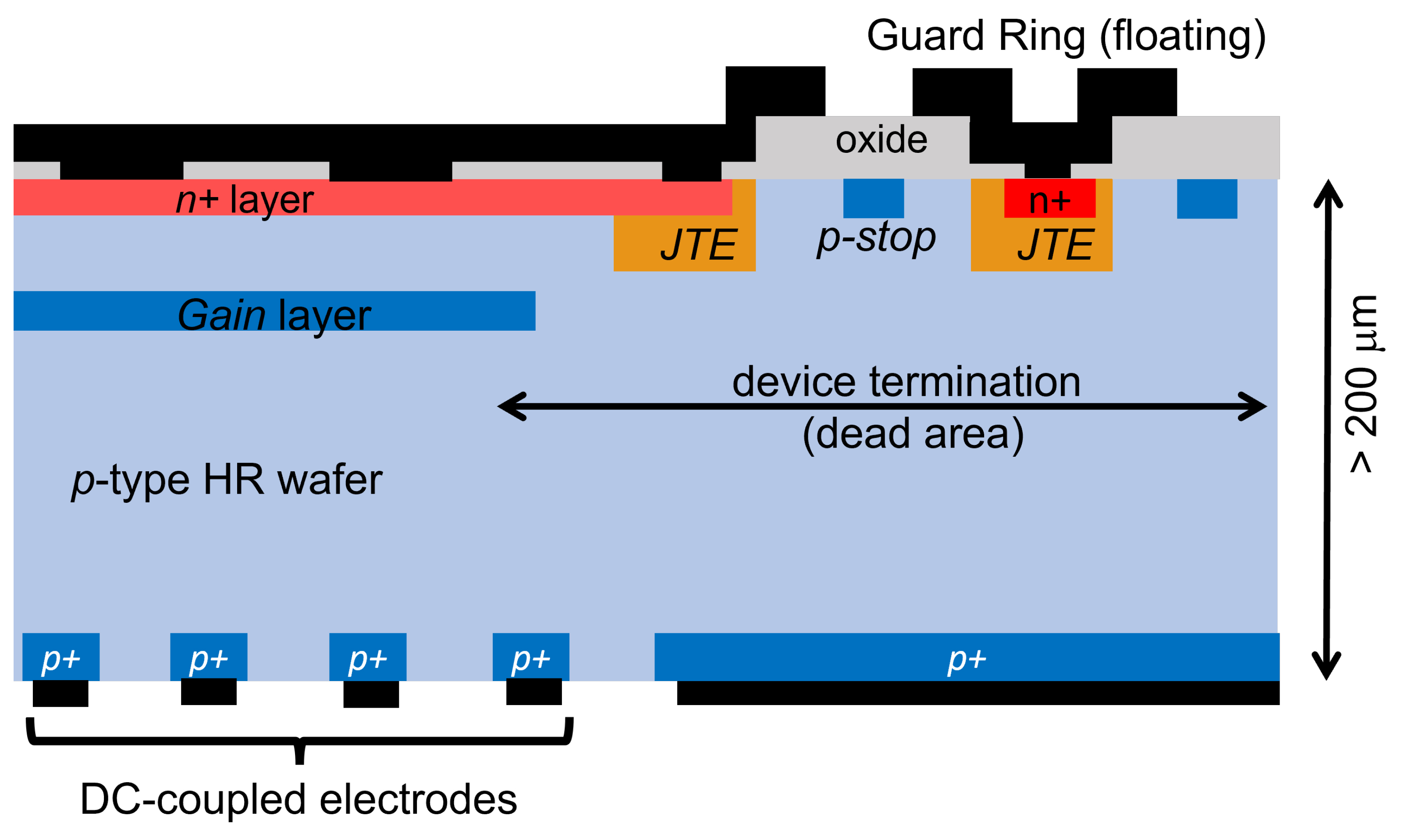
2. Trench-Isolated LGAD

In trench-isolated LGADs (TI-LGADs) [5], fine pitch n-electrodes are implanted close together and isolated by a trench. The approximately 1 μm wide trench replaces all the structures, such as p-stop and JTE, in the border region of a standard LGAD. Pixels, separated by trenches, are very close together which usually comes at the price of an increased interpixel capacitance. In TI-LGADs, this issue is mitigated by two factors: trenches, while electrically separating the pixel, also keep the interpixel capacitance lower than the case of the same geometry and different isolation (p-spray or p-stop). Second, interpixel capacitance becomes less important than the capacitance towards the back for thin substrates. This point applies also to standard LGADs. In TI-LGADs, JTE and p-stop are no longer needed, which benefits the fill factor. The doping profile of the shallow n+ phosphorus implant and of the p+ boron gain layer are unchanged with respect to the standard LGAD so that the breakdown voltage (and related operational point and gain factor) stays the same in the two cases. The devices have been fabricated by Fondazione Bruno Kessler (FBK, Trento, Italy), leveraging their experience in silicon etching and LGAD fabrications, and currently they are the only producer. Silicon etching is also used for 3D detectors, where columns are vertically etched into the substrate and doped by diffusion in furnaces. Aspect ratio (depth to diameter of columns) can be about 20:1; therefore, as the substrate thickness is about 100–150 μm, column diameters are in the order of 10 μm or just below. Trenches are used also in SiPMs [6] to optically isolate the single photon avalanche diodes (SPADs) so that the photons induced in one avalanche do not trigger parasitic avalanches in nearby SPADs (cross talk). To serve this purpose, trenches need to be filled with metal; a depth of only a few microns is required, which makes these trenches much more shallow than the columns in a 3D sensor. In TI-LGAD, trenches are quite similar to the SiPM ones, except that they are filled with oxide. A 7 μm dead border, instead of the usual few tens of microns, has been measured on these devices for an outstanding 75% fill factor for a 50 μm pitch sensor. Current–voltage characteristics are identical to those measured in standard LGAD devices with the same doping profiles. However, the current generation of TI-LGADs do not completely solve the problem as they do not yet achieve 100% fill factor which means further optimization may still be possible. Other LGAD-based devices can achieve 100% fill factor, as detailed below.

3. Inverted LGAD

An attempt to obtain high spatial resolution with a structure based on LGADs is the inverted LGAD (i-LGAD) [7]. It is based on keeping the n+ and gain layer on one side of the wafer, while the hole collecting electrodes are on the opposite side of the wafer [8][9] (a sketch is shown in Figure 3). The n+ and the gain layer will be uniformly implanted over a large area, interrupted only at the edge to allocate the proper termination for high voltage handling. The uniformity of the gain layer over a large area assures a 100% fill factor. On the opposite side, the hole collecting electrodes can be placed at a small pitch without detrimental effects on the uniform multiplication occurring at the opposite side of the wafer. A good spatial resolution is therefore achieved. However, the device, which operates in full depletion, requires double-sided processing of a high resistivity p-type wafer. To be processed in a standard clean room, wafers need to be about 200 μm thick for 4” wafers, and even thicker for 6” wafers. Such thicknesses, which will be entirely active as the device is fully depleted during operation, will spoil the timing capability of the LGAD. Timing resolution of only about 60 ps can be obtained for a 200 μm thick wafer. The i-LGAD can be used for imaging of particles that need some gain to be detected, for example soft X-ray, and only when timing information is not crucial. The researchers will finally consider sensors that truly deliver 100% fill factor, fast timing and good spatial resolution.
Figure 3. Sketch, not to scale, of a typical cross section of an i-LGAD, showing the main components as described in the text.

4. AC-LGAD

The capacitively coupled LGAD or AC-LGAD was the first LGAD-based sensor conceived to specifically address the issue of the dead region at the border of an LGAD pixel [10][11]. An AC-LGAD is made of a large uniform gain layer implanted below the n-implant, as in the standard LGAD. Where the two devices differ is that these two layers are uniformly implanted over the entirety of the active area; there is no interruption in the layers (except at the device termination). The n-implant is covered by a thin dielectric layer of approximately 100 nm (oxide, nitride or a stack of both) which is subsequently covered with metal electrodes that are then used to connect to the read-out electronics. The n+ is grounded at the edge, where the JTE is present as in the case of standard LGAD, and it is surrounded by the usual termination for the high voltage handling. A sketch is shown in Figure 4. The n-implant, which can be 10 or 100 times less doped than the n+ implant of a standard LGAD, has a sheet resistivity much larger than the n+ in the conventional LGAD and can be seen as a resistive layer. The metal electrodes create coupling capacitances over the resistive n+ in a similar fashion as in an AC-coupled silicon sensor. The whole device can be thought of as a distributed RC network, where R is given by the n+ layer and C by the the capacitances towards the back and toward the metal electrodes. As the oxide is very thin, the coupling capacitance dominates over the capacitance towards the back.
Figure 4. Sketch, not to scale, of a typical cross section of an AC–LGAD, showing the main components as described in the text.
The signal develops as in a standard LGAD; the electrons generated by the MIP are multiplied in the high electric field between the n+ and the gain layer. As the two layers are uniform, so are the electric fields and a 100% fill factor is achieved with uniform multiplication and no dead areas. The multiplied holes generate most of the signal during their drift to the p+ contact. The electrons are collected by the n+ implant and slowly drift to the DC contact at the border. The overall movement of signal electrons and holes capacitively induces a signal to the metal electrodes over the dielectric. Since the metal electrodes are separated from the n-layer by an insulator, they do not collect charge, and the signal pulse is bipolar. The fast signal “sees” a low impedance across the coupling capacitors and is fed to the read-out electronics before being spread to the neighbors. Nevertheless, a certain amount of cross talk exists due to the finite value of the interpixel resistance introduced by the n layer.
The cross talk between pixels can be exploited to increase the position resolution by interpolation at the expense of an increase of occupancy.
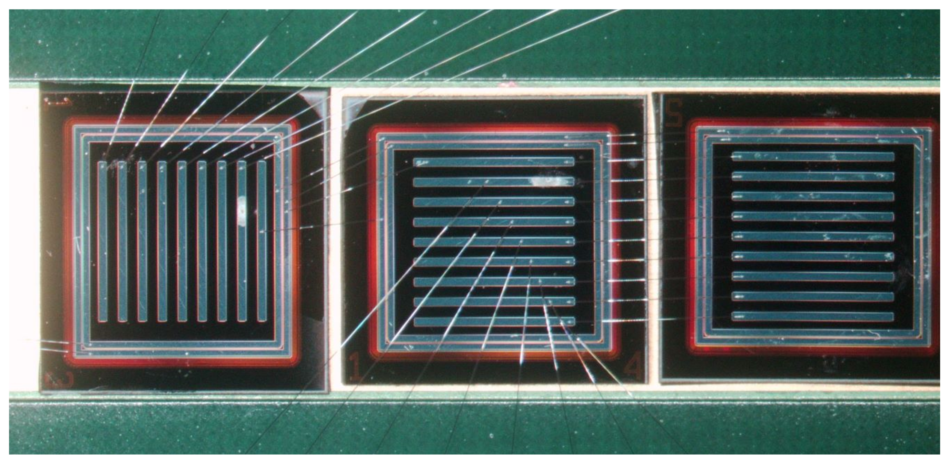
Tests in a laboratory setup, such as a Transient Current Technique (TCT) and confirmed at test beams, show a 100% fill factor, a timing resolution comparable to LGADs and spatial resolution at a level of 5% of the pitch [12][13]. As previously mentioned, some limitations occur as a result of the cross talk. On one hand, this is necessary to achieve excellent spatial resolution; on the other hand, it increases the occupancy so that the device in not useful in high event environments. In addition, experimental results suggest that the capacitance of long strips is quite high (the value of this capacitance is difficult to measure as it needs to be measured at high frequency). At the present stage of development, AC-LGADs in the shape of pixels or up to 1 cm long strips are excellent 4D detector candidates in low event rate environments. Pictures of LGADs recently fabricated at BNL are shown in Figure 5.
Figure 5. Picture of three 0.5 cm × 0.5 cm AC-LGAD devices, whose AC-coupled electrodes are in the shape of 0.5 cm long strips. Aluminum wire-bonds connect the metal electrodes to the read-out electronics (not shown) for testing purposes.

5. Deep-Junction LGAD

Another device that gives good 4D reconstruction is the deep-junction LGAD (DJ-LGAD) [14], which is currently under development. A sketch of a section of the device is shown in Figure 6. Its timing resolution is expected to be at the same level of an LGAD, while its spatial resolution is expected to be at the same level as a conventional strip or pixel detector. Therefore, it will not have the excellent spatial resolution of the AC-LGAD, but it can be used even in high rate of event environments. A deep junction, made by a large area of uniform n+ and p+ gain implants, sits a few microns from the surface where n+ DC coupled electrodes are placed.

In this new design, the multiplication region (where high electric fields are present) is contained between the buried n+ and p+ gain layer, while everywhere else the electric fields are well below the threshold for impact ionization. Electrons multiplied in this region then drift to be collected by the n+ electrodes at the interface; holes, as in any type of LGADs considered so far, drift toward the uniform back. Signal electrons generated by the MIPs in the few microns between the n+ electrodes and the n-gain layer do not cross the high field region and therefore do not get multiplied. On the other hand, signal holes generated here cross the high field region but contribute little to the signal, as they do not undergo significant multiplication. TCAD simulations suggest that the electric field within the gain layers just below the gap between pixels is slightly lower than below the pixels, but the effect can be mitigated by a proper design of the DC electrodes.
The DJ-LGAD can be fabricated by implanting both p+ and n+ gain layers on a 50-micron active layer and then by burying them under a few micron thickness of epitaxial layer. On the top of the layer, the DC coupled electrodes are finally defined. Another way is to implant the two gain layers on two different wafers which are then wafer-bonded together. The wafer carrying the n+ gain layer is then thinned down to a few microns and its surface processed to allocate the DC coupled electrodes. As the electric fields are low everywhere in the device except within the gain region, the JTE at the pixel border is no longer needed; p-spray or p-stop are instead still needed to isolate the n+ electrodes.
Figure 6. Sketch, not to scale, of a typical cross section of an DJ-LGAD, showing the main components as described in the text.

References

  1. Giacomini, G. Fabrication of Silicon Sensors Based on Low-Gain Avalanche Diodes. Front. Phys. 2021, 9, 618621.
  2. Ramo, S. Currents induced by electron motion. Proc. IRE 1939, 27, 584–585.
  3. Fernández-Martínez, P.; Flores, D.; Hidalgo, S.; Greco, V.; Merlos, A.; Pellegrini, G.; Quirion, D. Design and fabrication of an optimum peripheral region for low gain avalanche detectors. Nucl. Instrum. Methods Phys. Res. Sect. A Acc. Spectrom. Detect. Assoc. Equip. 2016, 821, 93–100.
  4. Dalla Betta, G.-F.; Pancheri, L.; Stoppa, D.; Henderson, D.; Richardson, J. Avalanche Photodiodes in Submicron CMOS Technologies for High-Sensitivity Imaging. In Advances in Photodiodes; InTechOpen: Rijeka, Croatia, 2011; ISBN 978-953-307-163-3.
  5. Paternoster, G.; Borghi, G.; Boscardin, M.; Cartiglia, N.; Ferrero, M.; Ficorella, F.; Siviero, F.; Gola, A.; Bellutti, P. Trench-Isolated low gain avalanche diodes (TI-LGADs). IEEE Electron Device Lett. 2020, 41, 884–887.
  6. Acerbi, F.; Paternoster, G.; Capasso, M.; Marcante, M.; Mazzi, A.; Regazzoni, V.; Zorzi, N.; Gola, A. Silicon Photomultipliers: Technology Optimizations for Ultraviolet, Visible and Near-Infrared Range. Instruments 2019, 3, 15.
  7. Dalla Betta, G.F.; Pancheri, L.; Boscardin, M.; Paternoster, G.; Piemonte, C.; Cartiglia, N.; Cenna, F.; Bruzzi, M. Design and TCAD simulation of double-sided pixelated low gain avalanche detectors. Nucl. Instrum. Meth. Phys. Res. A 2015, 796, 154–157.
  8. Heller, R.; Abreu, A.; Apresyan, A.; Arcidiacono, R.; Cartiglia, N.; DiPetrillo, K.; Ferrero, M.; Hussain, M.; Lazarovitz, M.; Lee, H.; et al. Combined analysis of HPK 3.1 LGADs using a proton beam, beta source, and probe station towards establishing high volume quality control. Nucl. Instrum. Methods Phys. Res. Sect. A Acc. Spectrom. Detect. Assoc. Equip. 2021, 1018, 165828.
  9. Milanesio, M.; Iacobucci, G.; Paolozzi, L.; Munker, M.; Cardella, R.; Gurimskaya, Y.; Martinelli, F.; Picardi, A.; Rücker, H.; Trusch, A.; et al. Gain measurements of the first proof-of-concept PicoAD prototype with a 55Fe X-ray radioactive source. Nucl. Instrum. Meth. Phys. Res. A 2023, 1046, 167807.
  10. Giacomini, G.; Chen, W.; D’Amen, G.; Tricoli, A. Fabrication and performance of AC-coupled LGADs. Jinst 2019, 14, P09004.
  11. Mandurrino, M.; Arcidiacono, R.; Boscardin, M.; Cartiglia, N.; Dalla Betta, G.F.; Ferrero, M.; Ficorella, F.; Pancheri, L.; Paternoster, G.; Siviero, F.; et al. Demonstration of 200-, 100-, and 50-μm pitch resistive Accoupled silicon detectors (RSD) with 100 fill-factor for 4D particle tracking. IEEE Electron Device Lett. 2019, 40, 1780–1783.
  12. Ott, J.; Letts, S.; Molnar, A.; Ryan, E.; Wong, M.; Mazza, S.M.; Nizam, M.; Sadrozinski, H.F.W.; Schumm, B.; Seiden, A.; et al. Investigation of signal characteristics and charge sharing in AC-LGADs with laser and test beam measurements. Nucl. Instrum. Meth. Phys. Res. A 2023, 1045, 167541.
  13. Apresyan, A.; Chen, W.; D’Amen, G.; Di Petrillo, K.F.; Giacomini, G.; Heller, R.E.; Lee, H.; Moon, C.S.; Tricoli, A. Measurements of an AC-LGAD strip sensor with a 120 GeV proton beam. Jinst 2020, 15, P09038.
  14. Apresyan, A.; Chen, W.; Gabriele, G.; Heller, R.; Mannelli, M.; Islam, R.; Lipton, R.; Tricoli, A. Buried Layer Low Gain Avalanche Diodes. Available online: https://indico.cern.ch/event/981823/contributions/4293564/attachments/2251204/3818882/BL-LGAD-TIPP.pdf (accessed on 10 February 2023).
More
Information
Contributor MDPI registered users' name will be linked to their SciProfiles pages. To register with us, please refer to https://encyclopedia.pub/register :
View Times: 561
Revisions: 2 times (View History)
Update Date: 06 Mar 2023
1000/1000
Video Production Service