Latest advances in the field of nanostructured photodetectors are considered, stating the types and materials, and highlighting the features of operation. Special attention is paid to the group-IV material photodetectors, including Ge, Si, Sn, and their solid solutions. Among the various designs, photodetectors with quantum wells, quantum dots, and quantum wires are highlighted. Such nanostructures have a number of unique properties, that made them striking to scientists’ attention and device applications. Nanostructures with quantum wells (QW) and quantum dots (QD) are very widely used to create photodetectors in the visible and infrared ranges. At the same time, for various applications, various semiconductor material systems are used that most fully satisfy the specific requirements for device structures: III–V (GaAs, AlGaAs, etc.), II–VI (CdHgTe), IV–IV (GeSi, GeSn, GeSiSn), and others.
1. Thin Film and Quantum Well Photodetectors
A quantum well is a very thin layer of one material with narrow bandgap is situated between two materials with wider bandgaps. As a result a potential step is formed. This potential well limits the motion of carriers in one direction while they are free to move in two other directions. When the width of the potential well is small enough, the energy spectrum of carriers becomes discrete and their motion in the thin layer becomes quantized. In this entry, the researchers will consider one of the simplest quantum well devices—quantum well photodetector.
The quantum well photodetector operation relies on the intersubband absorption within either the conduction band (for electrons) or the valence band (for holes). The principle of operation of a quantum well photodetector can be explained by the basic laws of quantum mechanics. The quantum well is equivalent to the classical problem of motion of a particle in a box. To obtain the energy spectrum of such particle the time independent Schrödinger equation should be solved.
The SiGe/Si material system almost immediately proved to be perspective for various applications of nanostructures in electronics and optoelectronics. Then, SiGeSn material system in various combinations of constituent elements became very promising, since within their framework it is possible to control the band gap and obtain direct-gap semiconductors. These materials can be used to create photodetectors, solar cells, and light-emitting devices, successfully competing with materials traditionally for optoelectronics based on III–V and II–VI compounds
[1][2][3][4][5][6][7][8][9][10].
GeSn techniques have drawn a lot of attention of Si-based technology in the last couple decades because the operating wavelengths range of this system spreads into the near infrared and short-wave infrared regions. Generally, scientific research on GeSn detectors has involved an increase in the past decade leading to the development of high-performance GeSn detectors. Today, there are several photodetectors based on Si-Ge. One of them is Ge-Si-Sn alloy, which is widely used in quantum well infrared photodetectors.
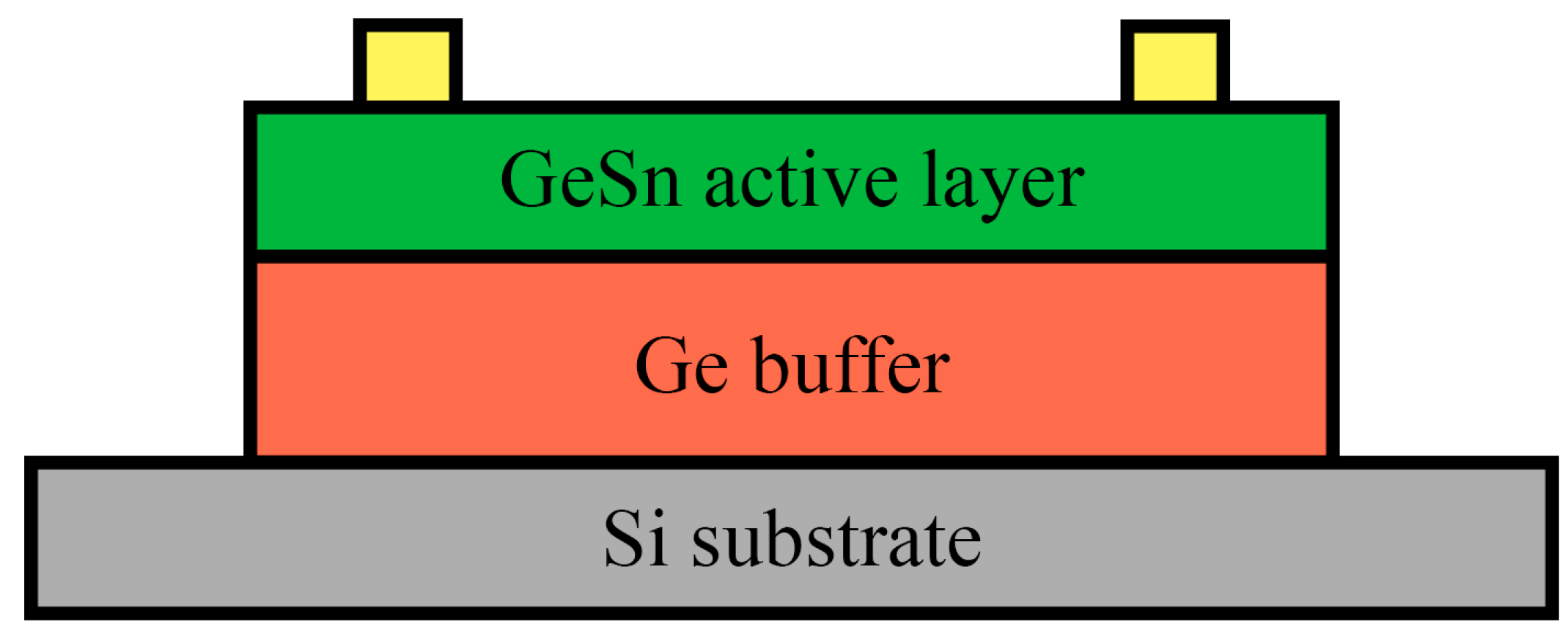
For example, in the work
[11] a photoconductor detector made of one layer of GeSn on Ge, and working in the range between 1.5–2 µm, was shown (
Figure 1).
Figure 1. Cross-section view of the one-layer GeSn on Ge photoconductor.
The photoconductor GeSn samples used in this photodetector were grown using a reduced-pressure chemical vapor deposition technology. A study has been conducted on this photoconductor using 0.9, 3.2, and 7% Sn. Electrical and optical characteristics under 300 to 77 K were measured and the results of the detectivity, dark current, and responsivity were observed and measured under equivalent conditions. It was noted that the higher the temperature the less the performance of this photodetector is, which is caused by the decrease in the number of thermally activated carriers. This leads to a higher noise currents, while the responsivity of the photoconductor shows the linear increase with applied voltage that is indicative of the photoconductive gain
[11].
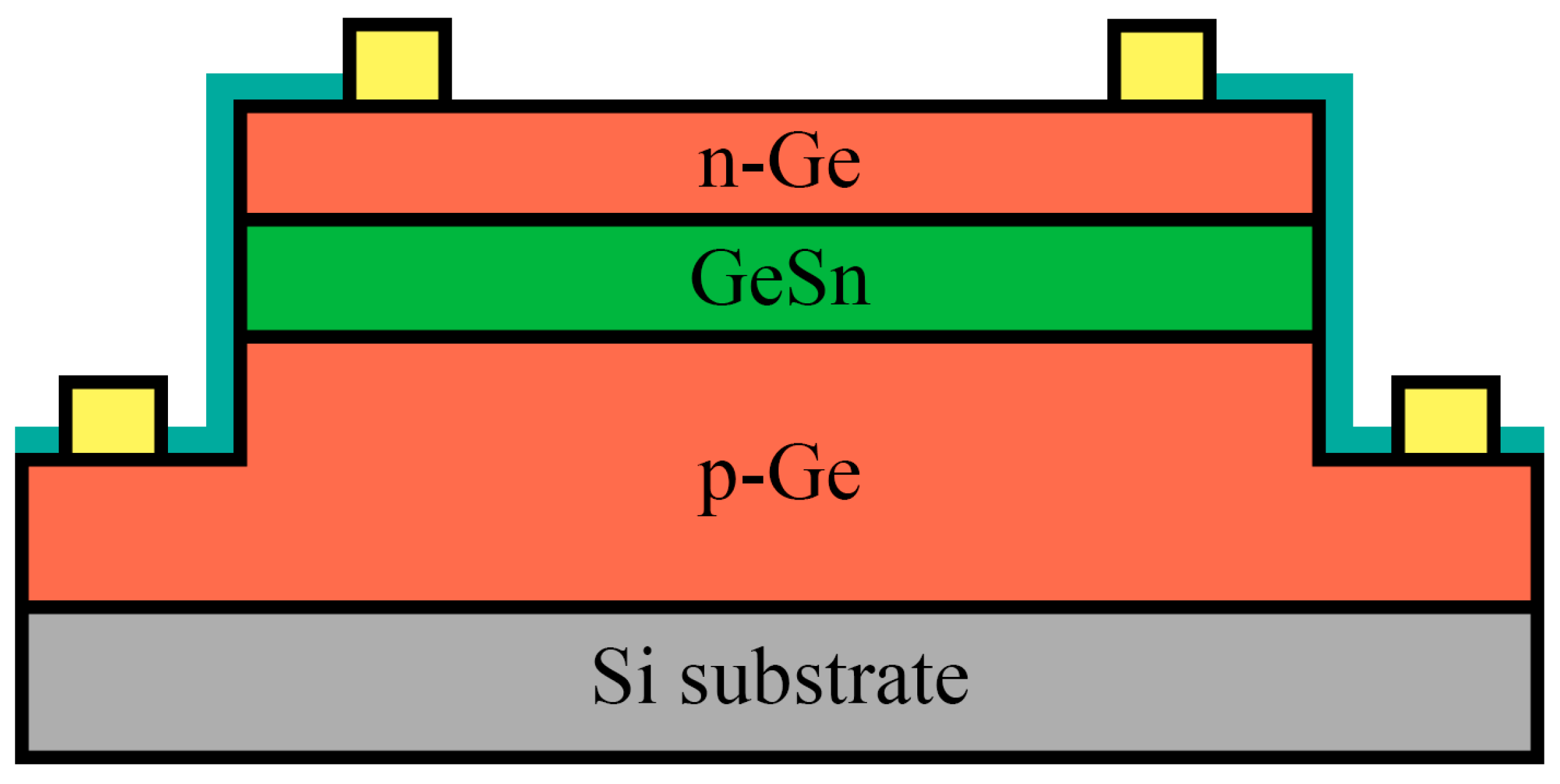
Another study has been made on GeSn alloy where a photodiode with one layer of Ge quantum well was investigated
[12]. The structure was grown on Si by molecular beam epitaxy.
Figure 2 shows a schematic cross-section of the p-i-n photodetector structure. The photodetector was fabricated with quasiplanar technology.
Figure 2. Schematic cross-section of the GeSn on Ge p-i-n photodiode structure.
The 1550 nm photodiode was investigated and the electrical and optical characteristics were measured under certain conditions. The dark current density of the photodiode increased by more than one order of magnitude, which was due to the high Sn concentration in this sample. The optical responsivity of the photodetector was also studied, which had shown the excellent quality of the fabricated GeSn layers.
A different study had been done based on one layer GeSn on Si
[13]. The GeSn samples were grown using reduced-pressure chemical vapor deposition technologies and mesa structures were fabricated by photolithography and wet chemical etch processes.
Figure 3 shows a schematic cross-sectional view of the photodetector.
Figure 3. Schematic cross-sectional view of the GeSn on Ge p-i-n photodetector.
There were two samples with 7% and 10% tin. Electrical and optical characteristics were investigated for both samples. The reverse current density increased with the temperature as a result larger number of thermally activated carriers. The 10% Sn device showed higher current densities compared to that of the 7% Sn device at equal conditions due to the narrower bandgap, which also resulted in the larger number of thermally excited carriers. Other parameters were also studied such as detectivity for both samples. They have shown very close values under the same conditions
[13].
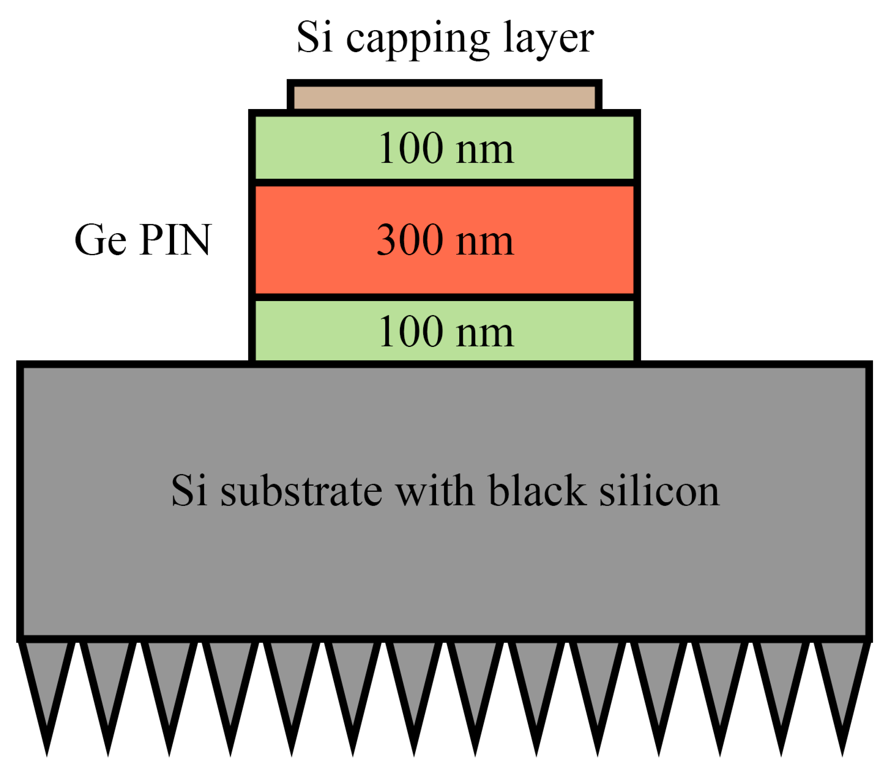
The next study with one layer structure used Ge on the Si system
[14]. The Ge p-i-n diode was grown on the Si substrate and covered by doped silicon capping layer. After the fabrication of p-i-n photodiode, the back side of the substrate was covered by black silicon. Optical power was induced from the rear side. The diameter of the mesa-structure was 400 µm, which is shown in
Figure 4.
Figure 4. Scheme of the black silicon Ge-on-Si photodiode.
It was noted that the black silicon nanostructure did not spoil the I-V characteristics and acted similar to waveguide structures. This article established that the application of black silicon light-trapping structures is a possible technology to increase the responsivity of Ge-on-Si photodiodes. Besides that, rather good combination of bandwidth and responsivity was achieved, making these structures viable for ultra-fast applications for communication
[14].
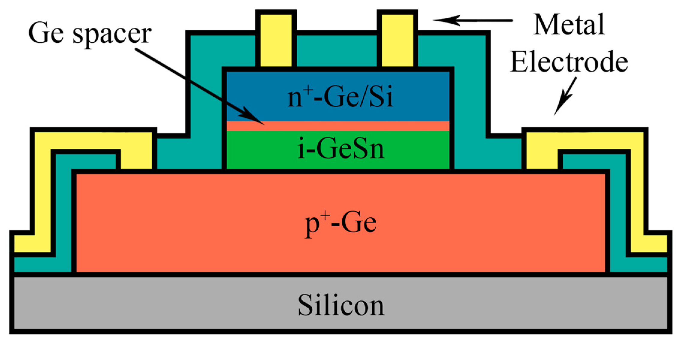
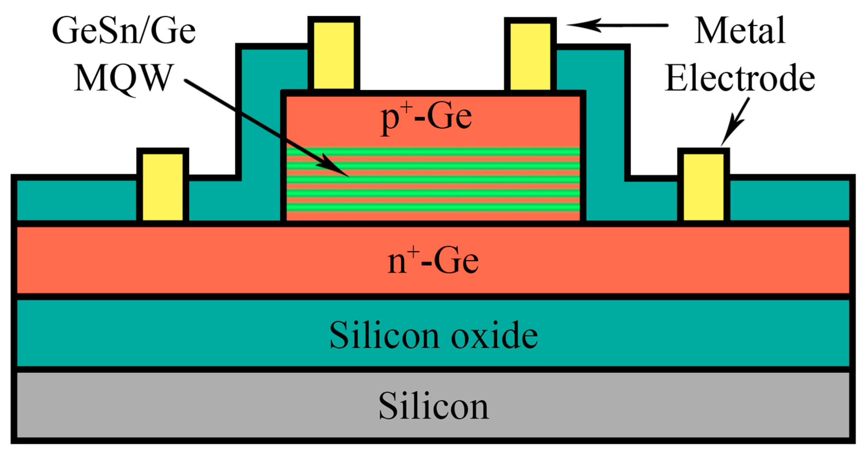
To enhance the absorption efficiency of the detector multiple layers with quantum wells may be used. One example with a GeSn/Ge multiple quantum wells (MQW) detector was shown in the recent work by Zhou et al.
[15]. The multilayer p-i-n structure was grown on a 300-mm Ge-buffered Si substrate by reduced pressure chemical vapor deposition.
Figure 5 shows a schematic diagram of the photodetector with a photon-trapping microstructure.
Figure 5. Schematic diagram of the multiple quantum wells GeSn/Ge photodetector with photon-trapping microstructure.
Characteristics investigations were made which have shown a flat photo response curve under a reverse bias voltage that indicates an efficient collection of photon-generated carriers and the capability of the photodetector regarding low-energy consumption. The dark current was investigated with and without a photon-trapping structure at room temperature. A low dark current density of 31.5 mA/cm
2 was achieved which is higher if compared with other photodetectors, and is also considered to be among the lowest for group-IV photodetectors. The dark current density increased to 45.2 mA/cm
2 at −1 V when the photon-trapping microstructure was incorporated. It was investigated and revealed that the increased dark current density mainly results from the increased surface leakage current introduced by the photon-trapping microstructure
[15].
To sum up, these works enable group-IV photodetectors to be very perspective for various infrared systems. It is also desirable to monolithically integrate these detectors with lasers, transistors, waveguides, modulators and other devices on one silicon platform. A lattice matched SiGeSn multiple quantum well structures should be developed to reduce the noise currents of this type of photodetectors in the future
[15].
2. Quantum Dot Photodetectors
A quantum dot is a nanometer-sized semiconductor particle. The concept of “artificial atoms”, or quantum dots, has emerged since the implement of molecular beam epitaxy and the first work on the reduced dimensionality of semiconductors. Quantum dots are widely used for their fully discrete energy spectrum and unique optical properties due to quantum size effects. They absorb and emit light of specific wavelengths if their energy spectra are matched. These wavelengths can be accurately controlled by changing size, shape or material composition of the particle. Hence, quantum dots are exploited in active layers for many widely-spread devices, for example, quantum dot displays and photon detectors.
Thus, an alternative to photodetectors based on quantum wells can be photodetectors with quantum dots. Such heterostructures are promising for photovoltaic applications and as receiving modules in fiber optic communication lines. Quantum dots have been successfully integrated in existing types of photodetectors, significantly enhancing their performance.
To realize all the potential advantages of photodetectors with quantum dots for the near-infrared range (increased sensitivity to normally incident radiation, high photoelectric multiplication factor, low thermal generation rate, narrow sensitivity range), the photosensitive region of the detector must contain an array of quantum dots with high density (on the order of 10
11–10
12 cm
−2)
[16][17][18][19].
The principles of operation of a photodetector with quantum dots are similar to those with quantum wells. The only difference is that in a quantum dot, the carrier is limited in its movement in all three directions, hence, zero-dimensional systems of carriers are realized
[20]. It is expected that due to this limitation, quantum dot photodetectors can provide a better performance, namely higher operating temperatures (due to longer carrier lifetimes), low dark current, and high photoelectric gain
[21], which ultimately translates into high sensitivity and detectability
[22]. In addition, due to different selection rules for the absorption of light in photodetectors with quantum dots, it becomes possible to absorb incident radiation polarized along the normal to the layers of quantum dots.
Silicon-based semiconductor materials with nanosized germanium inclusions have been actively studied since the early 1990s
[23][24]. Such nanoheterostructures with self-organizing germanium quantum dots on silicon, grown by molecular beam epitaxy, exhibit a number of new nanoscale effects (associated with low-dimensional quantization effects), which are promising from the point of view of their application in optoelectronic devices
[25][26][27][28][29][30].
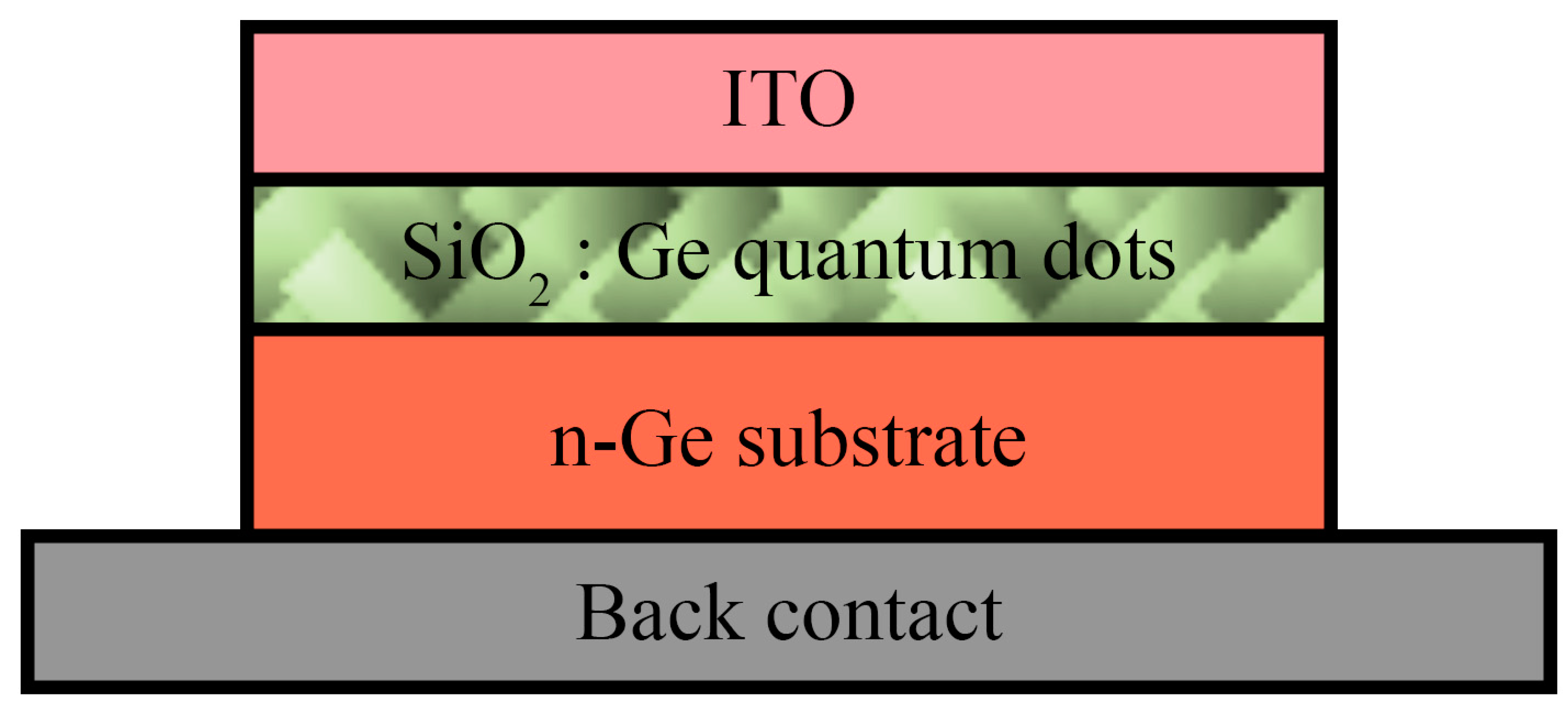
Starting with one layer of quantum dots, the following study shows an ultrathin layer photodetector with Ge quantum dots
[31]. A 13 nm active layer of Ge quantum dots in SiO
2 matrix was fabricated on n-Ge substrate with (100) orientation. Quantum dots diameters varied from approximately 3 to 8 nm. The schematic diagram of the photodetector is shown in
Figure 6.
Figure 6. Schematic diagram of the photodetector consisting of an ITO electrode and an active layer with quantum dots on top of an n-Ge substrate.
The current-voltage characteristics of the photodetector were studied at various temperatures which varied from 77 K to 300 K in the dark and under illumination with the 640 and 1550 nm light. Reducing the active layer thickness to an ultrathin regime produced a high dark current at ambient conditions. Rise and fall times below 10 ns and 25 ns were achieved at −1 V in the visible and near-infrared ranges which is very promising
[31]. This work has demonstrated that high quantum efficiency and fast response speed can be achieved in Ge quantum dot based photodetectors simultaneously at low voltage. Also, this work highlighted the importance of the thickness dependence of response speed in Ge quantum dot photodetectors.
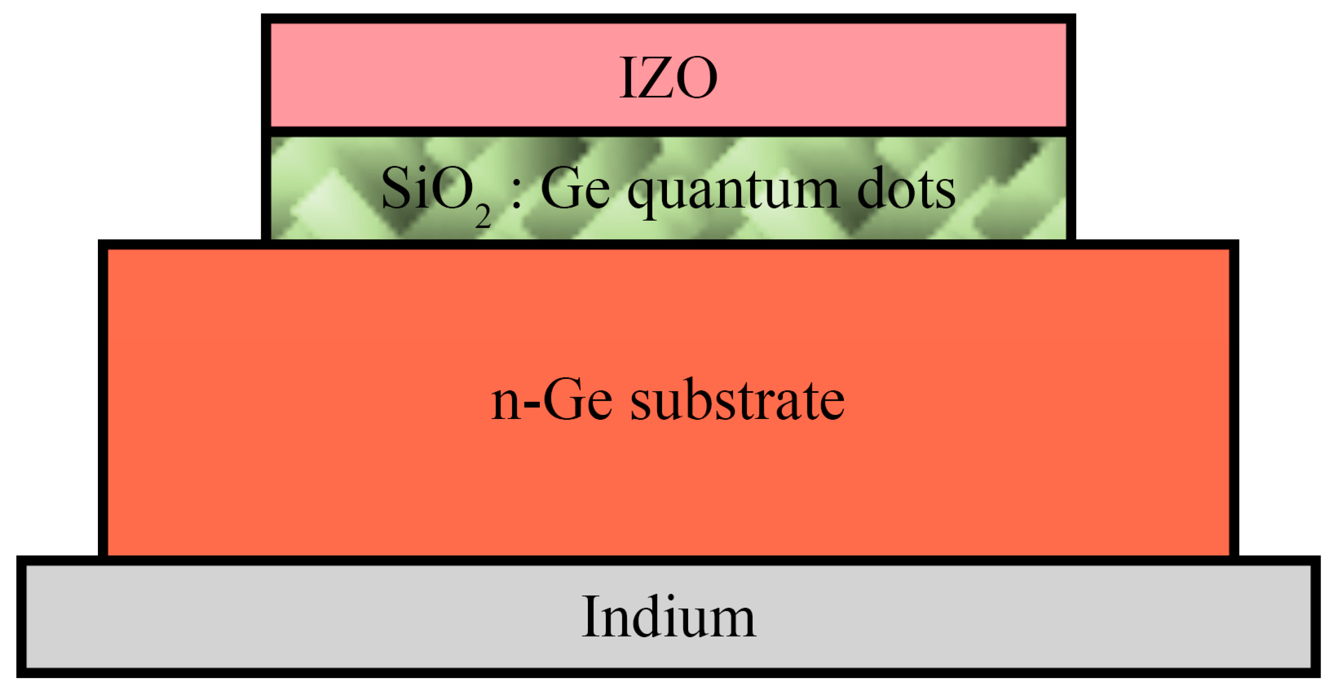
A new example of quantum dot photodetectors was shown in the work
[32]. Here a Ge quantum dot photodetector with one layer of quantum dots that has a thickness of 160 nm was fabricated. Ge and SiO
2 were cosputtered on the n-Ge substrate. The schematic diagram of the photodetector is shown in
Figure 7.
Figure 7. Schematic structure of the photodetector with Ge quantum dots in SiO2.
The current-voltage characteristics were investigated in the range of wavelengths from 400 to 1550 nm. Results on the responsivity, reflectance, and quantum efficiency of the detector were presented and it was shown that the detector had its best performance and efficiency between 500–600 nm. High detectivity was achieved at the temperature range of 100–300 K
[32].
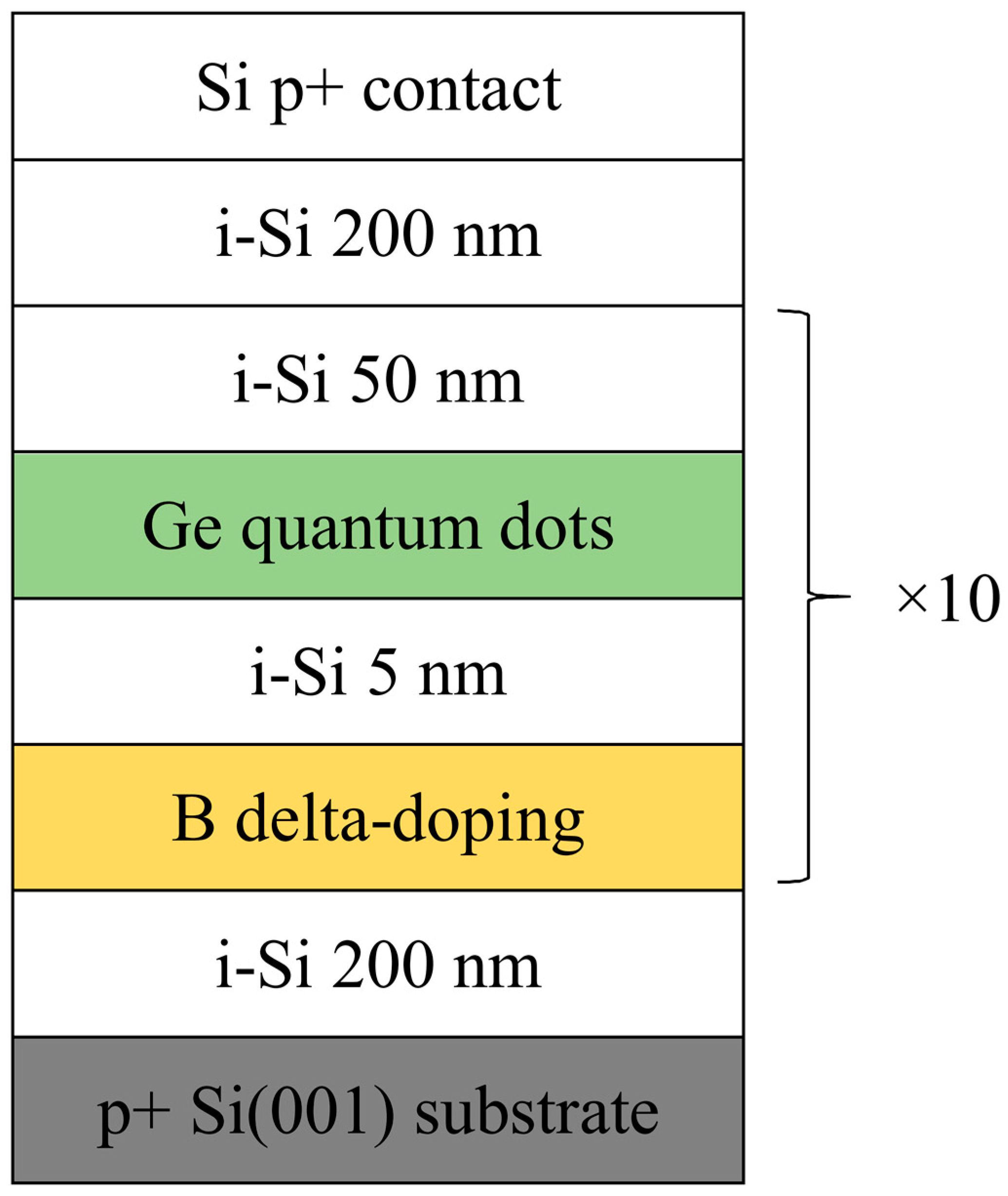
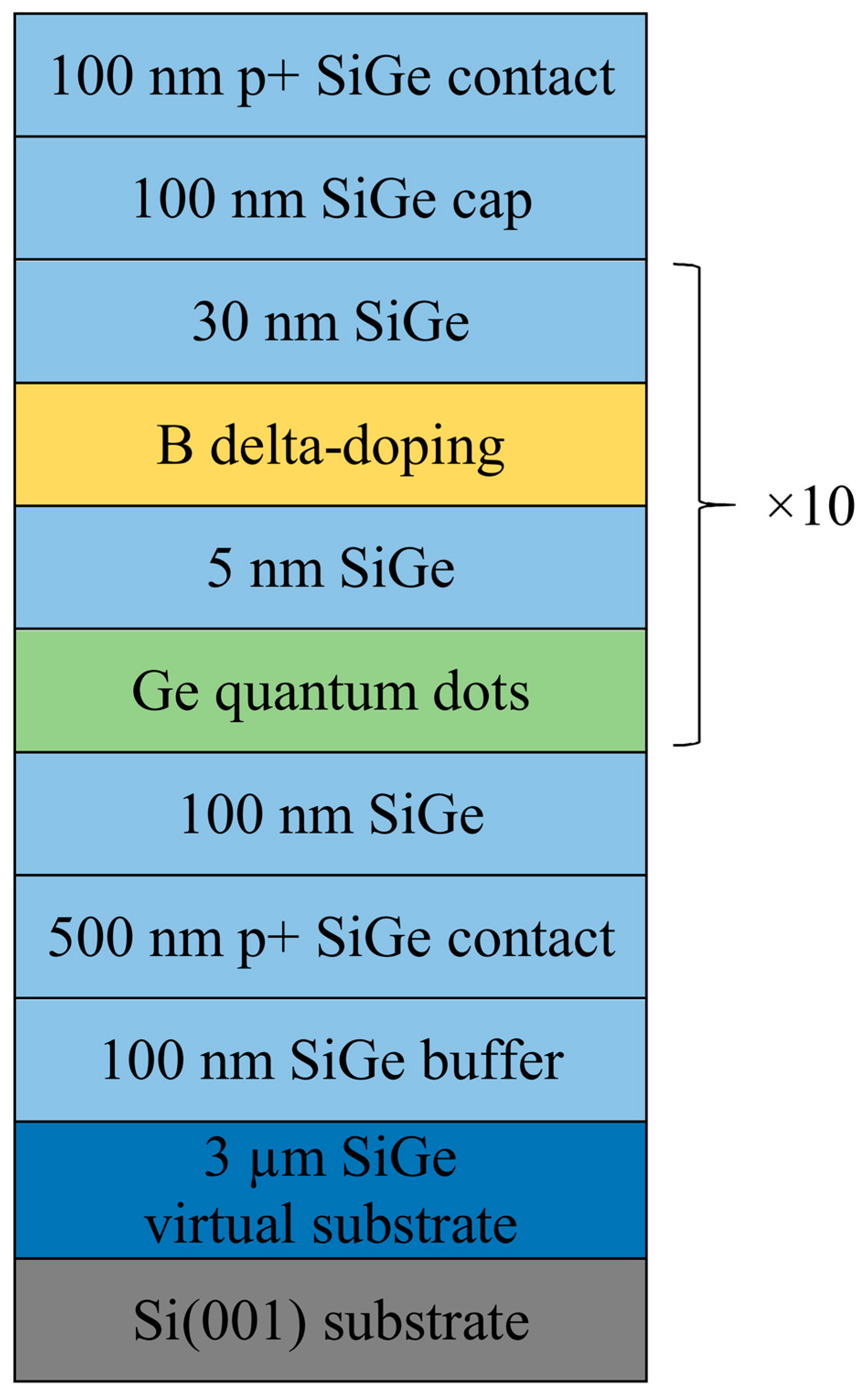
Next, a midinfrared photodetector based on Ge quantum dots in Si has been presented
[33]. The multilayer Si/Ge samples were synthesized by molecular beam epitaxy on the p
+-Si(001) substrate. The schematic design of the detector is shown in
Figure 8.
Figure 8. Schematic drawing of the Ge/Si photodetector with 10 layers of quantum dots.
Ten layers of germanium quantum dots separated by 50 nm silicon barriers served as active layers. Each Si barrier contained a boron delta-doping layer inserted 5 nm below the Ge-wetting layer. The active region was sandwiched between the 200-nm-thick intrinsic Si buffer and the cap layers. Finally, a 200-nm-thick p
+−Si top contact layer was deposited. The noise current, detectivity, and responsivity as a function of voltage and temperature were considered and the study has shown that such a device exhibited low dark current and operated until 200 K
[33].
One more study with a multilayer quantum dot photodetector was introduced next where the multiple germanium quantum dot layers were grown on Si
0.82Ge
0.18 virtual substrate
[34]. Ten layers of germanium quantum dots were separated by 35-nm Si
0.82Ge
0.18 barriers (
Figure 9).
Figure 9. Schematic diagram of the Ge/SiGe photodetector with 10 layers of quantum dots.
In this study another photodetector sample was fabricated based on pure silicon instead of SiGe for performance comparison purpose. Both samples have shown a responsivity in the whole mid-wave infrared range. Also, there was a significant improvement in the Ge/SiGe detector sensitivity over the wavelength region from 3 to 5 µm, as compared to the Ge/Si heterostructure. This is associated with the smaller hole effective mass in SiGe layers, which enables more efficient light absorption and photoexcited hole transportation. The photoconductive gain was studied and the noise characteristics were measured, and the SiGe detector has shown a larger gain, probably due to the increase of the hole mobility, and, therefore, the decrease of the hole transit time through the device.
The development of these works led to the emergence of the idea of using plasmonic effects and microresonators in order to enhance the properties of silicon-germanium photosensitive structures
[35]. These attempts have shown a significant increase in the photodetector parameters, such as resonant responsivity, when using such plasmonic structures
[36].
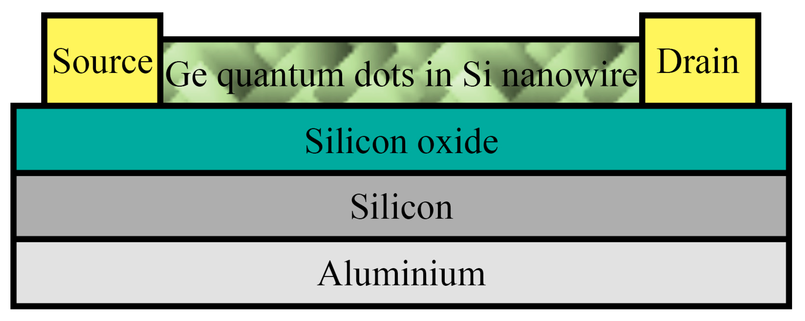
In work
[37], a silicon-on-insulator substrate was used for the growth of Ge quantum dots on silicon with subsequent fabrication of a quantum wire. Ge quantum dots were synthesized by molecular beam epitaxy. Quantum wires with the length of 10 μm and the width of 100 nm were fabricated by electron lithography.
Figure 10 shows the cross-section of the fabricated photodetector.
Figure 10. Schematic diagram of phototransistor with single Si nanowire decorated with Ge quantum dots.
This study demonstrated a simple and scalable fabrication process for achieving high-performance short-wave infrared photodetectors using Ge quantum dots in a single Si nanowire on CMOS-compatible SOI platforms. Moreover, the measurement of photocurrents with varying polarization of light revealed that the device can act as a polarization-sensitive photodetector
[37].
Thus, the performance of various types of photodetectors based on silicon, germanium, and tin is rapidly improving due to the dedicated efforts of many research groups. The bandwidth and quantum efficiency of such devices are comparable to those of their competitors in the face of devices based on III–V compounds and are sufficient for a number of applications. Thus, at present, no serious barriers are foreseen for the widespread use of Si-compatible group-IV-based nanostructured photodetectors.
 +1 credit