Your browser does not fully support modern features. Please upgrade for a smoother experience.
Submitted Successfully!
 +1 credit
Thank you for your contribution! You can also upload a video entry or images related to this topic.
For video creation, please contact our Academic Video Service.
| Version | Summary | Created by | Modification | Content Size | Created at | Operation |
|---|---|---|---|---|---|---|
| 1 | Benjamin Miller | -- | 2719 | 2022-12-28 16:12:48 | | | |
| 2 | Rita Xu | Meta information modification | 2719 | 2022-12-29 02:21:52 | | |
Video Upload Options
We provide professional Academic Video Service to translate complex research into visually appealing presentations. Would you like to try it?
Cite
If you have any further questions, please contact Encyclopedia Editorial Office.
Wang, P.; Miller, B.L. Waveguide-Enhanced Raman Spectroscopy. Encyclopedia. Available online: https://encyclopedia.pub/entry/39505 (accessed on 15 July 2026).
Wang P, Miller BL. Waveguide-Enhanced Raman Spectroscopy. Encyclopedia. Available at: https://encyclopedia.pub/entry/39505. Accessed July 15, 2026.
Wang, Pengyi, Benjamin L. Miller. "Waveguide-Enhanced Raman Spectroscopy" Encyclopedia, https://encyclopedia.pub/entry/39505 (accessed July 15, 2026).
Wang, P., & Miller, B.L. (2022, December 28). Waveguide-Enhanced Raman Spectroscopy. In Encyclopedia. https://encyclopedia.pub/entry/39505
Wang, Pengyi and Benjamin L. Miller. "Waveguide-Enhanced Raman Spectroscopy." Encyclopedia. Web. 28 December, 2022.
Copy Citation
Photonic chip-based methods for spectroscopy are of considerable interest due to their applicability to compact, low-power devices for the detection of small molecules. Waveguide-enhanced Raman spectroscopy (WERS) has emerged over the past decade as a particularly interesting approach. WERS utilizes the evanescent field of a waveguide to generate Raman scattering from nearby analyte molecules, and then collects the scattered photons back into the waveguide. The large interacting area and strong electromagnetic field provided by the waveguide allow for significant enhancements in Raman signal over conventional approaches.
photonics
spectroscopy
Raman
sorbent polymers
1. Introduction
There is an ever-increasing need for rapid yet low-cost detection of small molecules in many fields including point-of-care (POC) clinical diagnostics, environmental and industrial surveillance, and safety monitoring for food and other consumer goods. Sensors, defined here as devices that measure the presence and/or concentration of biological or chemical analytes, are already playing an important role in addressing these needs [1]. Most biosensing techniques with high specificity require covalently attached probes (antibodies, enzymes, DNA/RNA strands, aptamers, etc.) to act as specific biorecognition element for analytes [2][3][4][5]. Both “labeled” immunoassay techniques such as lateral flow assays and novel formats including lab-on-a-chip and label-free biosensors widely employed in POC detection [6] rely on the high affinity of antibodies toward their respective antigens for analyte recognition. However, the use of biopolymeric capture probes is less feasible when the molecular weight of the target analyte is small, in part because of the small binding that surface small molecules present (preventing the use of sandwich antibodies or labeling reagents). For label-free biosensors reliant on refractive index-based changes, small molecules present an additional challenge because they do not perturb the response of the sensor unless at high concentration. In the context of POC diagnostics, the most prominent set of diagnostically relevant molecules is the basic metabolic panel (BMP), which consists of glucose, calcium, sodium, potassium, carbon dioxide, chloride, BUN (blood urea nitrogen), and creatinine. These analytes range in molecular weight from 23 to 113 g/mol. Likewise, many of the analytes of interest industrially and in the context of environmental monitoring are small molecules.
To simplify the detection of small molecules, considerable research effort is being focused on vibrational spectroscopies, including infrared (IR) and Raman spectroscopy, as they directly identify and quantify molecules using vibrational characteristics uniquely determined by their molecular structure. Surface IR spectroscopy with various enhancement mechanisms, mainly attenuated total reflection infrared (ATR-IR) spectroscopy [7][8][9], infrared reflection absorption spectroscopy (IRAS or IRRAS) [10], and surface-enhanced infrared spectroscopy (SEIRAS) [8][9], have been used in the biosensing of small molecules [11]. However, since biological samples of interest are usually aqueous, IR spectroscopies suffer from the strong absorption of water over their mid-infrared (MIR, ~2–16 μm) operating wavelength (Figure 1). It is for this reason that Raman spectroscopy provides distinct advantages.
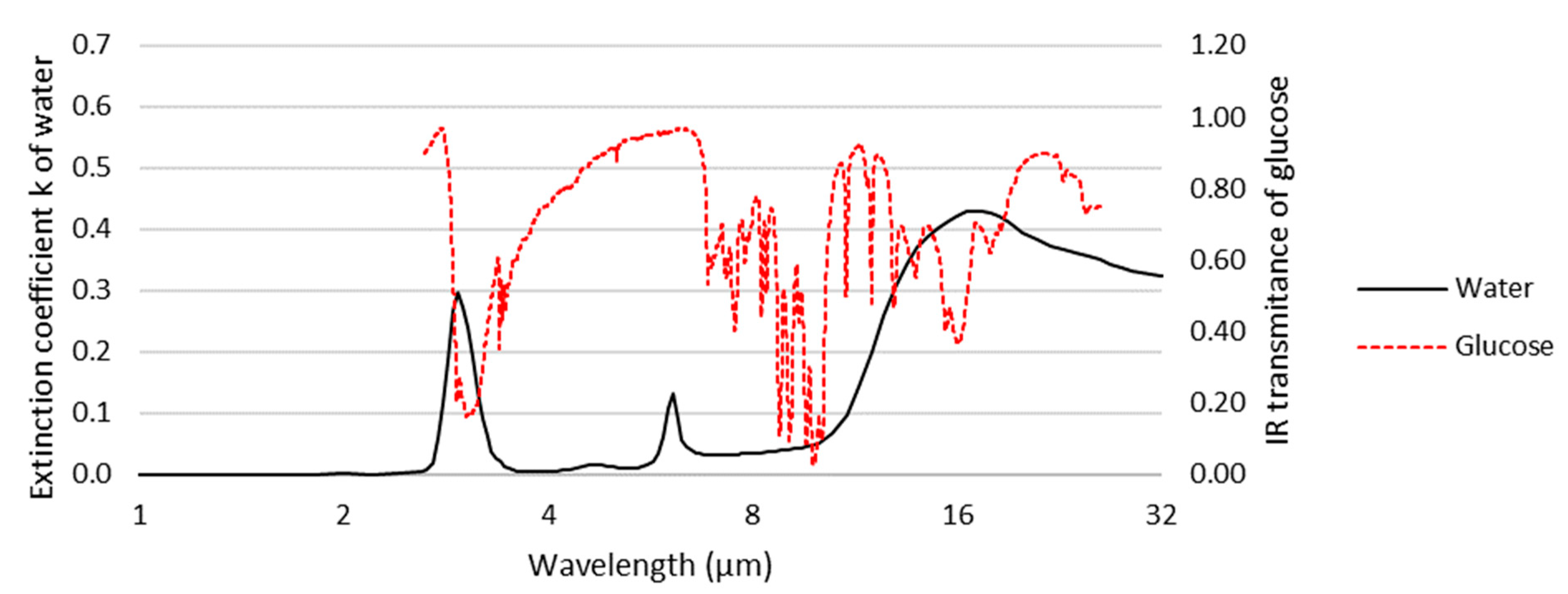
Figure 1. Extinction coefficient of water superimposed on the infrared spectrum of glucose (using data adapted from [12][13]). Water strongly absorbs at wavelengths corresponding to several of the characteristic bands of glucose, hindering its observation in aqueous samples by infrared spectroscopy.
Raman spectroscopy detects the inelastic Raman scattering of incident photons by analyte molecules [14]. The inelastically scattered photons have a wavelength shift (also known as a Stokes shift) from the wavelength of the incident photons, which is a function of the vibrational energies of the molecule undergoing analysis. By choosing an appropriate original wavelength of incident light (typically described as the “pump wavelength”), the scattered Raman signal can avoid the strong absorption wavelength range of water or other substrates. While this provides a distinct advantage over absorption spectroscopy, Raman spectroscopy also has a significant disadvantage in that Raman scattering is intrinsically very weak. For example, Rohleder et al. compared mid-IR and Raman spectroscopy in the quantitative analysis of serum and found that similar accuracy was achievable with both techniques, but the measurement time needed for Raman spectroscopy was 10 times longer (5 min) than for mid-IR spectroscopy (30 s) [15]. To address this problem, efforts have been made to enhance the scattering. Surface-enhanced Raman scattering (SERS) uses metal (mostly silver and gold) nanostructured substrates to locally enhance Raman scattering from analyte molecules by factors up to 106–1010 [16][17]. Despite many successful applications of SERS in biosensing [16][18][19] the reproducibility and robustness of the substrate are continuing concerns [17][20]. Moreover, SERS requires the analyte molecules to fall in optimally enhancing “hotspots” around the metal nanostructures, which may be difficult and inefficient when the analyte concentration is low and can also further increase the inconsistency of the detection. The hotspots may also get blocked by non-analyte molecules in complex samples [14].
WERS is an alternative, recently emerging [21] approach to enhancing the sensitivity of Raman that does not rely on metal nanostructures, thereby avoiding the challenges of SERS discussed above. WERS relies on the interaction of analytes with the evanescent field of a waveguide (discussed below) on a photonic chip. In contrast to SERS, where Raman scattering only comes from the enhancing hotspots, in WERS, analytes can interact with the evanescent field over the entire length of the waveguide, and the waveguide also collects and conducts the Raman scattering to the spectrometer. In theory, waveguides provide dozens-fold enhancement of Raman signal per cm [22]. For example, a direct experimental comparison of WERS with a standard confocal Raman microscope reported by Dhakal et al. [23] achieved more than four-orders-of-magnitude higher spontaneous Raman signal for WERS. As researchers discussed below, different configurations and the use of polymer sorbents can provide enhancements well beyond these levels (up to 108). The manufacture of waveguides for integrated photonics applications is mature and continuously improving because it relies on the same processes used in the microelectronics industry [24]. Waveguide structures can be produced with high consistency, avoiding the manufacturing scalability concerns that remain a challenge with SERS. Of course, as a label-free spectroscopic technique, there is also no need for perishable and expensive labels or probes.
WERS Basics
A dielectric optical waveguide is a structure that conducts electromagnetic waves, i.e., light. Waveguides constrain light and allow it to propagate along a “core” with higher refractive index compared to surrounding “cladding”, via total internal reflection. For example, an optical fiber is a type of waveguide. In this case, the core is glass (silica) or a polymer, and the cladding is either a polymer with a lower refractive index than the core or air. Figure 2 shows some common types of optical waveguides. Waveguides are useful in sensing in large part because the electromagnetic field of light conducted along the waveguide is not totally confined in the core region. It extends into the cladding, producing what is called an evanescent field. Light can interact with molecules falling in the evanescent field and cause Raman scattering. Early experiments with WERS used the electromagnetic field in the core, whereas the majority of recent efforts make use of the evanescent field for sensing.
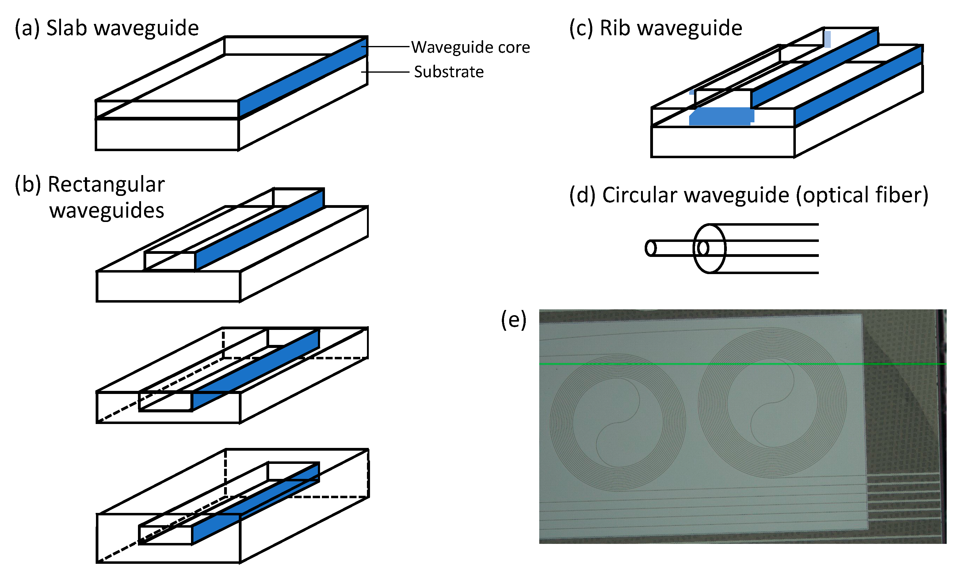
Figure 2. (a–d), adapted from [25]) Basic waveguide structures: slab waveguide, rectangular (channel/strip/wire) waveguide, and circular waveguide (optical fiber). Slot waveguides, not shown in this figure, consist of two rectangular waveguides positioned closely together in parallel. (e) Laser confocal microscope image of a WERS chip with spiral waveguides. The green line is a horizontal imaging reference.
2. Historical Development of WERS
As mentioned above, WERS was first demonstrated with liquid-core waveguides [26]. In an early report, a 10 to 25 m hollow fused quartz optical fiber with core diameter of ~75 μm was filled with benzene (C6H6) or tetrachloroethylene (C2Cl4) as the analyte. The waveguide conducted the pump laser and collected the Raman signal from the analyte core. Compared to conventional Raman spectroscopy, this technique enhanced the signal by factors of 102 to 103.
While such early experiments using optical fibers for WERS were impressive, implementation of the technique in a chip-based format paved the way for compact, low-cost sensing systems with significant advantages of size, weight, and power (SWAP) typical of integrated photonics [27]. A key demonstration of WERS by Levy in 1974 used a slab waveguide consisting of the analyte itself [28]. Methyl methacrylate (MMA) was made into a film a few μm thick and served as the core, both conducting the pump laser light and collecting the Raman signal of the material. Five years later, Rabolt [29] pushed the thickness of analyte thin film to as small as 1 μm without apparent background Raman from the substrate holding the film. These efforts demonstrated the feasibility of WERS, but also highlight the need to minimize Raman signals from the waveguide itself if one wants to detect an analyte external to the waveguide.
As a next step up in complexity from the analyte-core waveguides described above, Rabolt et al. [30] tested waveguides with a two-layer core. Two films together served as the core: one film was a thicker, known material with a well-characterized Raman spectrum, while the other film was only a few nm thick and actually the analyte to be tested. In this way, the analyte could be a molecular monolayer, and this Raman signal reflects the information about the bonds between the analyte and the thicker layer. In some ways, the analyte in this implementation effectively straddles the core and evanescent regions of the waveguide.
Similarly structured waveguides were used to measure the Raman signal of 8 nm polystyrene, a monolayer of the protein bovine albumin and dimyristoyl phosphatidylethanolamine (DMPE) Langmuir–Blodgett monolayers [31]. The substrate, core, and cladding were SiO2, ZnO, and air, respectively. The analyte was a thin film directly on the top of the ZnO core; however, here, it was considered to be located in the evanescent field instead of serving as a part of the core. The ZnO has higher refractive index than the polymer and biological analytes; thus, the local electric field intensity is higher and better enhances the Raman scattering. That is the reason why using a high-refractive-index core and exciting the analyte with the evanescent field became the mainstream of WERS. However, since the core is also exposed to the electromagnetic field, a potential disadvantage of this approach is that its emission will also be collected. Here, two peaks in the Raman spectrum of the ZnO core obscure the weak signal from analyte around their wavelength range. This result highlighted the need to optimize the material of the core to prevent core Raman signals from interfering with analyte signals.
For the example discussed above, Raman signals were collected using a lens positioned above the waveguide rather than at the waveguide end, as would be required for a fully integrated solution. In a follow-up to their work with ZnO core waveguides, the Greve group tested Si3N4 under the hypothesis that this would produce significantly less background as a core material than ZnO [32]. Here, the measurement geometry was also changed; this time they collected the Raman signal from the waveguide output. It was previously demonstrated both experimentally [33] and theoretically [34] by O’Connor and Tauc that Raman scattering excited by the evanescent field in the waveguide cladding can couple back to the guided mode. Although the original purpose of this finding was to bring notice to the fact that the optical fibers used in Raman spectroscopy generate background from the fiber’s core and cladding, it also laid the groundwork for later WERS studies using the evanescent field for sensing.
As hypothesized, Greve and colleagues found Si3N4 to have favorable characteristics for waveguide-based Raman measurements. This waveguide material has become the most commonly used waveguide materials for WERS, given its good collection efficiency and low background [35]. It is also convenient because of parallel developments in photonic integrated circuits (PICs) and in the computer industry. Complementary metal–oxide–semiconductor (CMOS) is a type of transistor which is critical for constructing electronic integrated circuit chips such as microprocessors and memory chips. Increasing the density of CMOS gives the chips higher computing power or bigger storage capacity. For years, Moore’s law has successfully predicted that technology developments in the industry would drive a doubling in the number of transistors on an electronic chip every 12–24 months. However, transistor scaling has reached a critical size limit due to electron leakage [36]. Thermal management has also become increasingly challenging as the density of electronic circuitry on computer chips has increased. Photonic circuits have the potential to overcome the bottlenecks imposed on electronic integrated circuits and continue pushing the boundaries of Moore’s law [37]. The fabrication process of photonic circuits can be executed with the CMOS fabricating techniques [38]. This CMOS compatibility is a key driver for the growth of PICs in other areas, including sensing.
Silicon-on-insulator (SOI) and silicon nitride (SiN) are the two most common materials used in the production of PICs, and they are compatible with standard CMOS fabrication methods [39]. As such, there is a large manufacturing infrastructure developed by the microelectronics industry that can be leveraged for PIC production. Standard SOI and SiN platforms are typically around 200–220 nm thick, although significant customization is possible. This design convention for waveguides can be tailored according to the specific needs of the application. Compared to SiN, SOI is theoretically usable but much less preferred for WERS due to silicon’s strong absorption at wavelengths typically used for WERS [23]. The intensity of Raman scattering is proportional to the fourth power of the excitation frequency [40]; hence, the wavelength chosen for the pump laser is as short as possible to maximize the intrinsically small Raman signal. This must be balanced against the fluorescence and absorption of the waveguide material, which increase at shorter wavelengths. Comparing the absorption coefficients of SiN (only showing Si3N4 here) and silicon (Figure 3), SiN has a significant advantage in this regard. However, the fluorescence/luminescence of SiN waveguides can be a problem; therefore, it is important to understand what contributes to the background luminescence of Si3N4 waveguides and how this can be reduced. Dhakal et al. [41] reported that SiN luminescence originates primarily from two sources: the narrow-band peak component is from impurities, especially hydrogen-based compounds and interstitial nitrogen, while the broad-band slowly varying component is from thermal fluctuations of the refractive index and momentum selection rule breaking in the amorphous material. For the slowly varying component, the researchers suggested that, if the material is more crystalline, the background spectrum may contract to narrower wavenumber ranges. Those findings remind researchers to pay attention to the details of waveguide fabrication, such as choosing appropriate chemical vapor deposition and annealing methods. Continued development of manufacturing processes have allowed both loss and luminescence in silicon nitride waveguides to be reduced to manageable levels [42].
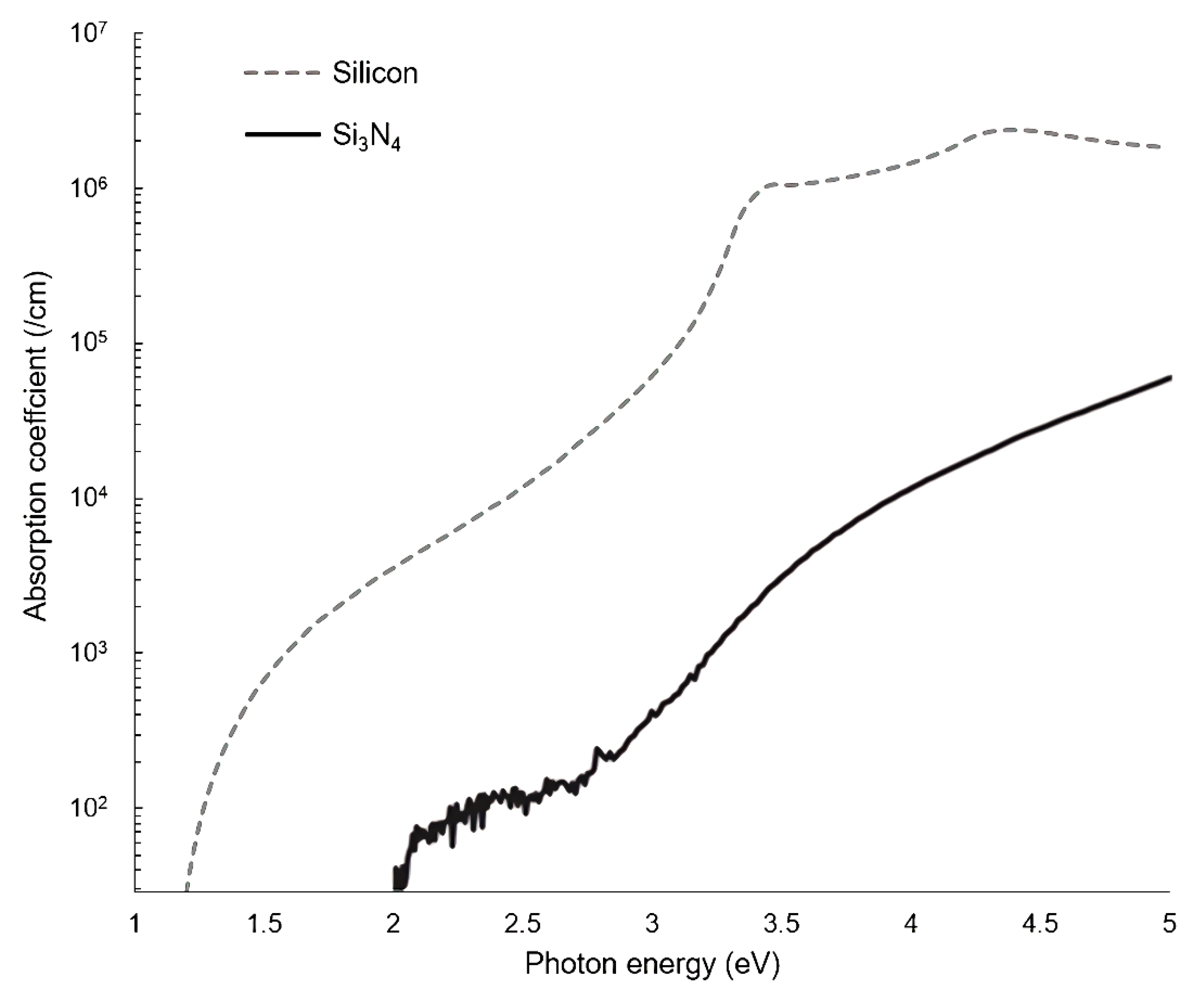
Figure 3. Absorption coefficient for Si3N4 and silicon as function of incident photon energy (E = hc/λ, where h is Planck’s constant, c is the speed of light, and λ is the wavelength; the x-axis is equivalent to 1240–250 nm; using data adapted from [43][44]).
3. Raman Emission Collected at the End of Waveguide vs. at the Surface of Waveguide
The theory developed above is focused on collecting Raman signals at the end of a waveguide. As seen in the discussion of early WERS experiments with slab waveguides, collecting from the top surface is also a possibility, and this has the advantage of not needing careful coupling of light from the waveguide into an optical fiber or microscope lens. To test the relative efficiencies of these two methods, Wang et al. [45] compared the collection of Raman emission from the waveguide end and the surface with a 110 nm Ta2O5 slab waveguide. Because of the geometry of the slab, the pump light was chosen to be in TM mode. The dipole under the electric field, therefore, oscillates perpendicular to the waveguide surface. In this case, they calculated that 76.3% of the Raman emission from a dipole will couple into the waveguide. For the remaining proportion, if a coverslip is put above the waveguide to reflect some of the escaping light back into the waveguide, the light coupled will increase by 17.8%. Moreover, collecting at the end accumulates the Raman signal from the analyte molecules all along the waveguide, whereas collecting at the surface only covers a relatively small area. Thus, for better enhancement, the collection site should be at the end, assuming that the propagation loss and coupling loss are not so large as to cancel the benefit. Rectangular waveguides have a substantially smaller top surface area than slab waveguides, which have a width considered to be infinite relative to the wavelength of light. As such, the mode profile of a rectangular waveguide is more similar to that of an optical fiber, making the coupling at the end of the waveguide more efficient.
References
- Rinken, T. State of the Art in Biosensors: Environmental and Medical Applications; Intech Open: London, UK, 2013.
- Zhang, W.; Guo, S.; Carvalho, W.S.P.; Jiang, Y.; Serpe, M.J. Portable point-of-care diagnostic devices. Anal. Methods 2016, 8, 7847–7867.
- Liu, J.; Geng, Z.; Fan, Z.; Liu, J.; Chen, H. Point-of-care testing based on smartphone: The current state-of-the-art (2017–2018). Biosens. Bioelectron. 2016, 132, 17–37.
- Prante, M.; Segal, E.; Scheper, T.; Bahnemann, J.; Walter, J. Aptasensors for point-of-care detection of small molecules. Biosensors 2020, 10, 108.
- Chen, S.Y.; Li, Z.; Li, K.; Yu, X.Q. Small molecular fluorescent probes for the detection of lead, cadmium and mercury ions. Coord. Chem. Rev. 2021, 429, 213691.
- Vashist, S.K.; Luong, J.H. Immunoassays: An overview. In Handbook of Immunoassay Technologies; Vashist, S.K., Luong, J.H., Eds.; Academic Press: Cambridge, MA, USA, 2018; pp. 1–18.
- Chittur, K.K. FTIR/ATR for protein adsorption to biomaterial surfaces. Biomaterials 1998, 19, 357–369.
- Sun, H.; Sun, C.; Ding, X.; Lu, H.; Liu, M.; Zhao, G. In situ monitoring of the selective adsorption mechanism of small environmental pollutant molecules on aptasensor interface by attenuated total reflection surface enhanced infrared absorption spectroscopy (ATR–SEIRAS). J. Hazard. Mater. 2021, 403, 123953.
- Hu, Y.; Chen, Q.; Ci, L.; Cao, K.; Mizaikoff, B. Surface-enhanced infrared attenuated total reflection spectroscopy via carbon nanodots for small molecules in aqueous solution. Anal. Bioanal. Chem. 2019, 411, 1863–1871.
- Hoffmann, F.M. Infrared reflection-absorption spectroscopy of adsorbed molecules. Surf. Sci. Rep. 1983, 3, 107–192.
- Boujday, S.; Lamy de la Chapelle, M.; Srajer, J.; Knoll, W. Enhanced vibrational spectroscopies as tools for small molecule biosensing. Sensors 2015, 15, 21239–21264.
- Hale, G.M.; Querry, M.R. Optical constants of water in the 200-nm to 200-μm wavelength region. Appl. Opt. 1973, 12, 555–563.
- D-Glucose Infrared Spectrum. Available online: https://webbook.nist.gov/cgi/inchi?ID=C2280446&Type=IR-SPEC&Index=1#IR-SPEC (accessed on 22 September 2022).
- Smith, E.; Dent, G. Modern Raman Spectroscopy: A Practical Approach; John Wiley & Sons: Hoboken, NJ, USA, 2019; p. 16.
- Rohleder, D.R.; Kocherscheidt, G.; Gerber, K.; Kiefer, W.; Köhler, W.; Möcks, J.; Petrich, W.H. Comparison of mid-infrared and Raman spectroscopy in the quantitative analysis of serum. J. Biomed. Opt. 2005, 10, 031108.
- Langer, J.; de Aberasturi, D.J.; Aizpurua, J. Present and future of surface-enhanced Raman scattering. ACS Nano 2019, 14, 28–117.
- Fan, M.; Andrade, G.F.; Brolo, A.G. A review on the fabrication of substrates for surface enhanced Raman spectroscopy and their applications in analytical chemistry. Anal. Chim. Acta 2011, 693, 7–25.
- Schlücker, S. Surface-Enhanced raman spectroscopy: Concepts and chemical applications. Angew Chem. 2014, 53, 4756–4795.
- Fan, M.; Andrade, G.F.; Brolo, A.G. A review on recent advances in the applications of surface-enhanced Raman scattering in analytical chemistry. Anal. Chim. Acta 2020, 1097, 1–29.
- Jaworska, A.; Fornasaro, S.; Sergo, V.; Bonifacio, A. Potential of surface enhanced Raman spectroscopy (SERS) in therapeutic drug monitoring (TDM). A critical review. Biosensors 2016, 6, 47.
- Holmstrom, S.A.; Stievater, T.H.; Kozak, D.A.; Pruessner, M.W.; Tyndall, N.; Rabinovich, W.S.; McGill, R.A.; Khurgin, J.B. Trace gas Raman spectroscopy using functionalized waveguides. Optica 2016, 3, 891–896.
- Stievater, T.H.; Khurgin, J.B.; Holmstrom, S.A.; Kozak, D.A.; Pruessner, M.W.; Rabinovich, W.S.; McGill, R.A. Nanophotonic waveguides for chip-scale Raman spectroscopy: Theoretical considerations. In Chemical, Biological, Radiological, Nuclear, and Explosives (CBRNE) Sensing XVII, Proceedings of the SPIE Defense + Security, Baltimore, MD, USA, 17–21 April 2016; SPIE: Bellingham, WA, USA, 2016; Volume 9824, pp. 8–13.
- Dhakal, A.; Wuytens, P.C.; Peyskens, F.; Jans, K.; Thomas, N.L.; Baets, R. Nanophotonic waveguide enhanced Raman spectroscopy of biological submonolayers. Acs Photonics 2016, 3, 2141–2149.
- Luan, E.; Shoman, H.; Ratner, D.M.; Cheung, K.C.; Chrostowski, L. Silicon photonic biosensors using label-free detection. Sensors 2018, 18, 3519.
- Zhang, X.J.; Hoshino, K. Chapter 5—Optical transducers: Optical molecular sensing and spectroscopy. In Molecular Sensors and Nanodevices: Principles, Designs and Applications in Biomedical Engineering, 2nd ed.; Academic Press: Cambridge, MA, USA, 2019; pp. 231–309.
- Walrafen, G.E.; Stone, J. Intensification of spontaneous Raman spectra by use of liquid core optical fibers. Appl. Spectrosc. 1972, 26, 585–589.
- Coldren, L.A.; Verrinder, P.A.; Klamkin, J. A Review of Photonic Systems-on-Chip Enabled by Widely Tunable Lasers. IEEE J. Quantum Electron. 2022, 58, 1–10.
- Levy, Y.; Imbert, C.; Cipriani, J.; Racine, S.; Dupeyrat, R. Raman scattering of thin films as a waveguide. Opt. Commun. 1974, 11, 66–69.
- Rabolt, J.F.; Santo, R.; Swalen, J.D. Raman spectroscopy of thin polymer films using integrated optical techniques. Appl. Spectrosc. 1979, 33, 549–551.
- Rabolt, J.F.; Santo, R.; Schlotter, N.E.; Swalen, J.D. Integrated optics and Raman scattering: Molecular orientation in thin polymer films and Langmuir-Blodgett monolayers. IBM J. Res. Dev. 1982, 26, 209–216.
- Kanger, J.S.; Otto, C.; Slotboom, M.; Greve, J. Waveguide Raman spectroscopy of thin polymer layers and monolayers of biomolecules using high refractive index waveguides. J. Phys. Chem. 1996, 100, 3288–3292.
- Kanger, J.S.; Otto, C.; Greve, J. Stimulated Raman gain spectroscopy of thin layers using dielectric waveguides. J. Phys. Chem. 1996, 100, 16293–16297.
- O’Connor, P.; Tauc, J. Raman spectrum of optical fiber waveguide—Effect of cladding. Opt. Commun. 1978, 24, 135–138.
- O’Connor, P.; Tauc, J. Light scattering in optical waveguides. Appl. Opt. 1978, 17, 3226–3231.
- Raza, A.; Clemmen, S.; De Goede, M.; Ali, R.; Hua, P.; Garcia-Blanco, S.M.; Honkanen, S.; Wilkinson, J.S.; Baets, R. The performance of high-index-contrast photonics platforms for on-chip raman spectroscopy. In Proceedings of the European Conference on Integrated Optics (ECIO’2018), Valencia, Spain, 30 May–1 June 2018; pp. 35–37.
- Mack, C. The multiple lives of Moore’s law. IEEE Spectr. 2015, 52, 31.
- Margalit, N.; Xiang, C.; Bowers, S.M.; Bjorlin, A.; Blum, R.; Bowers, J.E. Perspective on the future of silicon photonics and electronics. Appl. Phys. Lett. 2021, 118, 220501.
- Morton, P.A.; Bowers, J.E.; Khurgin, J.B. ‘Beyond Moore’s Law’ Photonic Integrated Circuits for RF Photonics and Sensing Systems; Morton Photonics Inc.: West Friendship, MD, USA, 2018.
- Rahim, A.; Ryckeboer, E.; Subramanian, A.Z.; Clemmen, S.; Kuyken, B.; Dhakal, A.; Raza, A.; Hermans, A.; Muneeb, M.; Dhoore, S.; et al. Expanding the silicon photonics portfolio with silicon nitride photonic integrated circuits. J. Light. Technol. 2017, 35, 639–649.
- Albrecht, A.C. On the theory of Raman intensities. J. Chem. Phys. 1961, 34, 1476–1484.
- Dhakal, A.; Wuytens, P.; Raza, A.; Le Thomas, N.; Baets, R. Silicon nitride background in nanophotonic waveguide enhanced Raman spectroscopy. Materials 2017, 10, 140.
- Tyndall, N.F.; Kozak, D.A.; Pruessner, M.W.; Goetz, P.G.; Rabinovich, W.S.; Stievater, T.H.; Fahrenkopf, N.M.; Antohe, A. A Low-Loss, Broadband, Nitride-Only Photonic Integrated Circuit Platform. In Proceedings of the Quantum 2.0, Boston, MA, USA, 13–16 June 2022; Optica Publishing Group: Washington, DC, USA, 2022; p. QTu4B-5.
- Hiller, D.; Zelenina, A.; Gutsch, S.; Dyakov, S.A.; López-Conesa, L.; López-Vidrier, J.; Estradé, S.; Peiró, F.; Garrido, B.; Valenta, J.; et al. Absence of quantum confinement effects in the photoluminescence of Si3N4–embedded Si nanocrystals. J. Appl. Phys. 2014, 115, 204301.
- Optical Properties of Silicon. Available online: https://www.pveducation.org/pvcdrom/materials/optical-properties-of-silicon (accessed on 11 October 2022).
- Wang, Z.; Zervas, M.N.; Bartlett, P.N.; Wilkinson, J.S. Surface and waveguide collection of Raman emission in waveguide-enhanced Raman spectroscopy. Opt. Lett. 2016, 41, 4146–4149.
More
Information
Subjects:
Optics
Contributors
MDPI registered users' name will be linked to their SciProfiles pages. To register with us, please refer to https://encyclopedia.pub/register
:
View Times:
1.6K
Revisions:
2 times
(View History)
Update Date:
29 Dec 2022
Table of Contents


Notice
You are not a member of the advisory board for this topic. If you want to update advisory board member profile, please contact office@encyclopedia.pub.
OK
Confirm
Only members of the Encyclopedia advisory board for this topic are allowed to note entries. Would you like to become an advisory board member of the Encyclopedia?
Yes
No
${ textCharacter }/${ maxCharacter }
Submit
Cancel
Back
Comments
${ item }
|
${ item.createdUser.fullName }
${ item.createdAt }
${ item.vote }
${ item.reply }
Delete
${ reply.createdUser.fullName }
${ reply.createdAt }
${ reply.vote }
Delete
There is no reply to this comment~
${ item.replyTextCharacter }/${ item.replyMaxCharacter }
Submit
Cancel
More
No more~
There is no comment~
${ textCharacter }/${ maxCharacter }
Submit
Cancel
${ selectedItem.replyTextCharacter }/${ selectedItem.replyMaxCharacter }
Submit
Cancel
Confirm
Are you sure to Delete?
Yes
No