Your browser does not fully support modern features. Please upgrade for a smoother experience.
Submitted Successfully!
 +1 credit
Thank you for your contribution! You can also upload a video entry or images related to this topic.
For video creation, please contact our Academic Video Service.
| Version | Summary | Created by | Modification | Content Size | Created at | Operation |
|---|---|---|---|---|---|---|
| 1 | Fangzhou Xia | -- | 3383 | 2022-12-14 18:59:37 | | | |
| 2 | Sirius Huang | Meta information modification | 3383 | 2022-12-15 03:44:39 | | |
Video Upload Options
We provide professional Academic Video Service to translate complex research into visually appealing presentations. Would you like to try it?
Cite
If you have any further questions, please contact Encyclopedia Editorial Office.
Xia, F.; Youcef-Toumi, K. Basic Principles of Atomic Force Microscopy. Encyclopedia. Available online: https://encyclopedia.pub/entry/38784 (accessed on 17 July 2026).
Xia F, Youcef-Toumi K. Basic Principles of Atomic Force Microscopy. Encyclopedia. Available at: https://encyclopedia.pub/entry/38784. Accessed July 17, 2026.
Xia, Fangzhou, Kamal Youcef-Toumi. "Basic Principles of Atomic Force Microscopy" Encyclopedia, https://encyclopedia.pub/entry/38784 (accessed July 17, 2026).
Xia, F., & Youcef-Toumi, K. (2022, December 14). Basic Principles of Atomic Force Microscopy. In Encyclopedia. https://encyclopedia.pub/entry/38784
Xia, Fangzhou and Kamal Youcef-Toumi. "Basic Principles of Atomic Force Microscopy." Encyclopedia. Web. 14 December, 2022.
Copy Citation
Visualization of biomedical samples in their native environments at the microscopic scale is crucial for studying fundamental principles and discovering biomedical systems with complex interaction. The study of dynamic biological processes requires a microscope system with multiple modalities, high spatial/temporal resolution, large imaging ranges, versatile imaging environments and ideally in-situ manipulation capabilities. Development of new Atomic Force Microscopy (AFM) capabilities has made it such a powerful tool for biological and biomedical research.
atomic force microscopy
nanotechnology
mechanobiology
high-speed imaging
material property mapping
1. Introduction
Many fundamental discoveries from biomedical research arise from studies at the microscopic scale. The human body is composed of trillions of cells, which interact with trillions of microscopic living organisms like bacteria and virus every day. Microorganisms are ubiquitous and typically too small to be seen by the naked eye. To study these microscopic organisms and their interactions, the development of microscopy instruments has become essential for scientists to conduct fundamental research.
The study of complex samples in biomedical research can benefit significantly from advanced microscopy instruments. Taking the virus-cell interaction as an example, viruses can infect all types of life forms, from animals and plants to microorganisms. Although viruses exhibit many modes of infection, all of them are parasites that must infiltrate hosts in order to replicate. Most viruses are enveloped in a membrane such as the coronavirus. The presence of this envelope has a profound influence on the attributes of the virus, especially when encountering the plasma membrane of the host cell. Virus-receptor interactions play a key role in viral internalization. The viral attachment proteins can be viewed as the “key” that unlocks host cells by interacting with the “lock”, which are the receptors on the host cell surface. These lock-and-key interactions results in the formation of pores that allow passage of the viral core into the interior of the cell. To better understand these interactions, microscopic visualization techniques that can resolve mechanical properties and molecular species with high-temporal and high-spatial resolution in liquid are needed.
Microscopy techniques relevant to biomedical research primarily includes optical microscopy, (cryo)-electron microscopy and scanning probe microscopy. They corresponds to three types of interactions with the sample including electromagnetic radiation (light at different wavelength), electron scattering, and mechanical force. As shown in Figure 1, different types of microscopy techniques have their own resolution capabilities, target modalities, operation environments and suitable sample preparation steps. Depending on the application requirements, corresponding techniques can be selected. In many demanding applications, multiple techniques are combined for in-situ characterization of samples. Note that many other microscopy techniques are also available such as X-ray crystallography and nuclear magnetic resonance imaging, which are more relevant for studies in other fields such as physics and material science and therefore not discussed in details here.
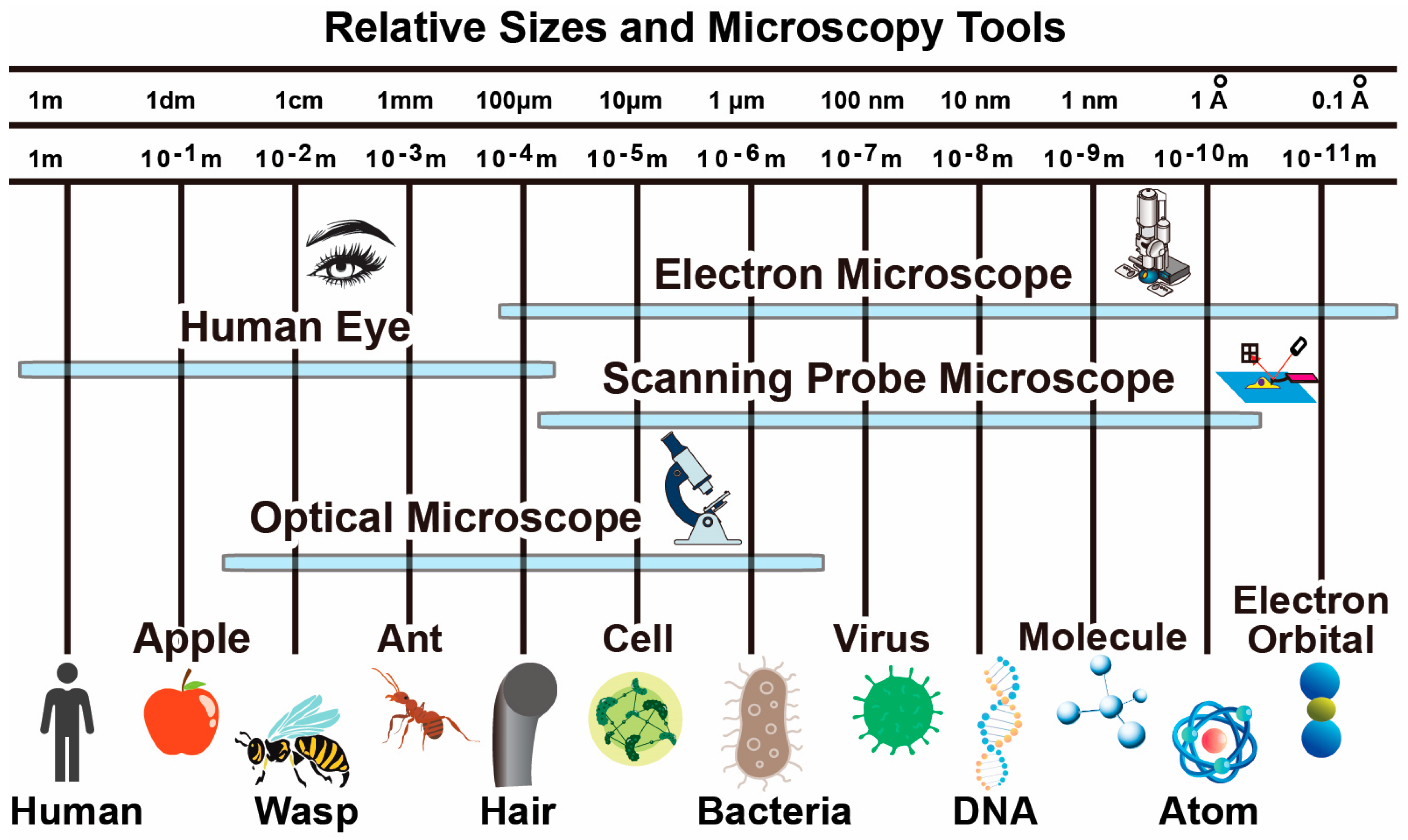
Figure 1. Typical size of biological objects and resolution capabilities of microscopy techniques.
Optical microscopy is widely used by microbiologists to study micrometer scale objects. Depending on the type of light source configurations, optical microscopy can in general be classified into bright field, dark field and fluorescence. Bright field microscopy is the most widely used tool to image biological samples typically stained and fixed on glass slides. In this mode, the background is bright whereas the sample specimen is dark. To improve the spatial resolution, dark field microscopy with more sophisticated optical setup is utilized where the sample is bright and the background is dark. The resolution is limited by diffraction as governed by the Rayleigh criterion. Fluorescence microscopy can further improve spatial resolution by highlighting target structure with fluorescence dye to emit light at various wavelength in response to ultra-violet light source. Better contrast can be obtained as the neighboring structure does not emit light and multiple colors can be obtained.
Even with fluorescence microscopy, the spatial resolution is still limited to above one hundred nanometers. This resolution allows the study of cells but prevents the study of smaller samples such as viruses and DNA molecules. Moreover, light-based optical techniques cannot directly obtain mechanical property information, such as stiffness and adhesion. Therefore, another microscopy instrument is needed to overcome such limitations.
Electron microscopy is an alternative technique that can create subnanometer resolution images. Electron microscopes create images by shining a beam of electrons onto the sample and measure the properties of back-scattered, secondary or transmitted electrons to create contrast images. It is widely used in nanotechnology research on (semi)conductive samples. The main limitation for its application on biological sample is the required operation environment in vacuum and sample coating for conductivity. Biological samples can easily be damaged during the process required before imaging. To better preserve the sample structure integrity, cooling the aqueous biological sample down to cryogenic temperature to form amorphous ice allows better imaging of the biological sample structure down to near-atomic resolution. However, such processing forbids the observation of dynamic changes in the biological samples and also cannot provide mechanical property information.
Atomic Force Microscopy (AFM), a member of the Scanning Probe Microscopy (SPM) family, is a great complementing tool to resolve the aforementioned limitations. First, AFM is a versatile tool that can operate in ambient air, high vacuum and liquid environments, which makes it an ideal imaging technique for biomedical research. Biological samples can be imaged in buffer solution by AFM, which is helpful to preserve specimens in their native states. Second, an AFM in its basic form can obtain 3D topography information [1] by scanning a cantilever probe over the sample surface. AFM typically has subnanometer out-of-plane resolution and in-plane resolution on the order of several nanometers. It can resolve DNA double helix [2] or even atomistic events at the atomic lattice step edges in the right conditions [3]. The probe-sample interactions can be of various nature and result in the deflection change of a micro-cantilever. As a result, the mechanical interaction between the probe and the sample can also be easily captured to create material property mappings. Third, AFM probes used for imaging also offer a more direct way to mechanically manipulate the sample compared to optical tweezers and electron beam based fabrication (e.g., lithography, welding, evaporation, etc.). These characteristics of AFM make it an attractive tool for biomedical applications. Scanning Tunneling Microscope (STM) is another type of SPM system using a rigid conductive tip and the tunneling current to image conductive samples with atomic resolution. It is used more often in material science research instead of biomedical research due to more stringent requirements of the sample and imaging environments. A summary of the aforementioned microscopy categories is summarized in Table 1. Notice that values provided are for typical systems while specialized implementation can significantly change the characteristics of the instrument. For example, in high-speed AFM imaging to be discussed in details later, the frame rate can be significantly increased at the cost of a smaller imaging area.
Table 1. Comparison of Main Microscopy Techniques.
| Microscopy | Optical | SEM | TEM | AFM | STM |
|---|---|---|---|---|---|
| Resolution | 200 nm | 10 nm | 0.2 nm | 2 nm | 0.1 nm |
| Typical Image Size | 1000 μm | 1000 μm | 100 μm | 100 μm | 0.5 μm |
| Typical Frame Rate | 100 FPS | 20 FPS | 20 FPS | 0.1 FPS | 0.1 FPS |
| Main Modality | 2D image | 3D image | 2D projection | 3D Topography | 3D density of states |
| Environment | vacuum, air, liquid | vacuum | vacuum | vacuum, air, liquid | vacuum, air |
Compared to optical and electron microscopy techniques, conventional AFMs also have several limitations. First, the AFM imaging speed is relatively slower due to the serial mechanical scanning process of the cantilever probe. Second, to avoid damage to the fragile biological samples, AFM operation is more complicated as it involves mode selection and controller parameter tuning to ensure good imaging quality. Third, AFM cannot sense electromagnetic spectrum directly in its native form (e.g., light color), which may contain important material property information. On the microscopic scale, color can be considered as the absorption/reflection spectrum of the sample material across a wide range of wavelength. A pair of electromagnetic wave emission and detection source is typically required for the measurement of such spectrum, which is not natively available in a conventional AFM setup. Consequently, it is challenging to use conventional AFMs in its basic form to meet the challenging demands in biomedical research. Fortunately, the AFM technique has evolved rapidly to realize new capabilities and overcome existing limitations based on experimental needs by proper modification of the AFM system and combination with other techniques.
2. AFM Basic Principles
A typical AFM can create 3D topography images with a range over hundreds of microns at subnanometer resolution. The out-of-plane resolution of AFM can reliable resolve single atomic layer steps of graphene, which is around 0.35 nm. The system vibration level and performance of the nano-positioning system is the main limiting factor of the out-of-plane resolution. The in-plane resolution of AFM is mostly limited by the probe tip radius and modes of operation with a typical value on the order of several nanometers. In specialized conditions, subnanometer resolution is possible [3], while in other cases where metallic tip coating is applied, the resolution is limited to tens of nanometers. To realize nanoscale topography imaging capabilities, a conventional AFM is primarily composed of three subsystems. They are the cantilever probe, the nano-positioning system, and controller electronics, as shown in Figure 2.

Figure 2. Principle illustration of a conventional AFM including a cantilever probe with optical beam deflection sensor and piezo-acoustic resonance excitation, a nanopositioning system, and an imaging motion controller.
2.1. Cantilever Probe
A flexible microcantilever probe with a tip, sensors and actuators is used to interact with the sample. A typical probe is composed of a base support chip, a microcantilever, and a sharp tip. Probes are typically made with silicon, silicon dioxide or silicon nitride material created through nanofabrication processes. In most cases, the cantilever deflection is measured using an optical beam deflection system to achieve sub-nanometer resolution. A laser source and a quadrature photodetector work together to measure the free end angle change of the cantilever, which is proportional to the deflection at small angles. A piezo actuator can be used to acoustically excite the resonance of the cantilever for dynamic mode operation. Going beyond conventional implementation, additional sensing methods have also been investigated including astigmatic detection, interferometry, optomechanical sensing, piezoresistivity, and piezoelectricity. Alternative actuation methods include piezoelectric, photothermal, thermomechanical, electrostatic, and electromagnetic principles. A more detailed review of these principles is available in [4].
For advanced applications, both the tip and the micro-cantilever of the AFM probe can be upgraded. For example, the tip geometry and material can be modified to image high-aspect ratio samples with sharp tip, perform nano-indentation using spherical tip, improve laser detection performance with reflective gold coating or create electrical property mapping with conductive tip. For the micro-cantilever, active elements can be embedded into the structure to realize sensing and actuation with some of the aforementioned principles such as piezoresistivity, piezoelectricity, etc. Such active probes can help to enable new AFM capabilities with details in review [5]. For biomedical applications, selected principles can be mixed and matched based on experimental needs.
2.2. Nano-Positioners
A nanopositioning system regulates the relative position between the probe tip and the sample surface. Depending on the modes of operation, the deflection or oscillation characteristics of the cantilever are regulated by controlling the relative spacing between the probe tip and the sample surface. Either the probe or the sample can be scanned to create the relative motion needed for imaging.
For practical implementation, a large-range (i.e., several millimeters) coarse XYZ positioner driven by stepper motor is used to identify area of interest on the sample and engage the probe tip with the sample. A flexure-constrained scanner driven by piezoelectric actuators creates the relative to cover the scanning motion with a range over hundreds of microns at subnaometer resolution. Depending on the application needs, scanners may be exchanged to have different resolution, range and bandwidth characteristics.
2.3. Controller Electronics
The AFM control system is crucial to ensure good imaging performance and avoid damaging fragile biological samples. Modern AFM control systems are mostly implemented on Field Programmable Gate Array (FPGA) for the main logic. Signal conditioning circuits and driver electronics developed on custom printed circuit boards are used as the analog front end to interface with sensors and actuators. In more advanced imaging modes such as amplitude or frequency modulated dynamic modes, additional signal processing modules such as lock-in amplifiers and phase-locked loops are needed. During imaging experiments, the gains of the proportional-integral-derivative controller should be tuned by the users to ensure a good tracking performance.
2.4. AFM Imaging Modes
The AFM hardware can be operated in a number of modes for imaging purpose to extract various sample information. Depending on the dynamics of probe-sample interaction, they can in general be classified into four categories including contact modes, dynamic modes, jumping modes and hybrid modes.
The contact modes category is the most straightforward to understand where the cantilever deflection signal during tip-sample interaction is directly recorded or regulated during imaging. While scanning the sample, the lateral force can be measured through probe twisting to obtain friction coefficient and surface roughness information. Using a conductive probe and a biased sample, electrical properties such as voltage, current, conductance, capacitance and resistance of the sample can be measured through modes such as Scanning Voltage Microscopy (SVM), Scanning microwave microscopy (SMM), Photoconductive/Conductive Atomic Force Microscopy (PC/CAFM), Scanning Spreading Resistance Microscopy (SSRM) and scanning capacitance microscopy (SCM). The sample temperature can also be imaged with temperature-sensitive filament located near the tip through Scanning Thermal Microscopy (SThM) [6]. As the probe scans over the sample, electrical bias can be applied to excite the piezoelectric response of the material that can be measured with the cantilever deflection, giving rise to piezoresponse force microscopy (PFM). Such mechanical response can also be triggered through photothermal processes with radiation-based heating through infrared light, which corresponds to the mode of AFM-based infrared spectroscopy (AFM-IR). In addition to force responses, the optical response of the material enhanced by the plasmon effect at the probe tip and the sample surface can be utilized for Tip-Enhanced Raman Spectroscopy (TERS).
In dynamic mode AFM, the cantilever probe resonance is excited to generate a sinusoidal cantilever deflection signal during probe-sample interaction [7]. During imaging, the amplitude, phase, or frequency of this signal can be regulated to control the interaction and create contrast maps. The term “tapping mode” is often used when the interaction force is within the repulsive region of the Lennard-Jones potential between the probe tip and the sample. For the attraction region, the term “non-contact mode” AFM is used [8]. Multiple resonance frequencies can be excited simultaneously to create material property contrast mapping with more details discussed later. To measure surface potential, Kelvin Probe Force Microscopy (KPFM) technique is developed. This mode creates a topography imaging using tapping mode first and utilize the measured topography to create a repeated scan in an “interleaved” manner to characterize the surface potential and remove contribution from the topography. To measure electrostatic or magnetic force instead of surface potential, the Electrostatic Force Microscopy (EFM) and Magnetic Force Microscopy (MFM) operating in non-contact mode can be utilized. In addition to potential measurement, the cantilever tip can be utilized to enhance the localized electromagnetic field enhancement that helps to boost spatial resolution. When combined with cantilever resonance excitation, target signal with vibration signature can be extracted for spectroscopy purpose to enable the scattering-type Scanning Near-field Optical Microscopy (s-SNOM) mode. As an example in this category, the nanoscale Fourier Transformation Infrared Spectroscopy (nano-FTIR) injects dithering feature using the cantilever oscillation into the near-field signal to be distinguished from far-field noise signal using lock-in amplifiers.
In jumping mode, the resonance of the probe is not deliberately excited. Instead, the probe and the sample are brought into intermittent contact at a frequency much lower than the first cantilever resonance frequency with the peak deflection regulated using a controller. The jumping mode has many other names that can be a bit confusing, such as off-resonance dynamic mode or peak force tapping mode [9], etc. The simplest form of jumping mode is the force volume mode where a force versus distance curve is created at each location [10]. Contact mechanics model can be fitted to the obtained data to extract material property information including the snap-to-contact motion [11]. To improve the speed of imaging, Bruker company developed the patented Peak Force Tapping mode using sinusoidal approach curves during imaging. A corresponding quantitative nanomechanical property mapping mode named PFQNM is also developed. Ringing mode is an extension of the PFT mode where the residual vibration from each probe-sample interaction cycle can also be analyzed to extract additional material property information. Considering the complex interaction between soft samples and the cantilever probe tip involving adhesion, ringing mode is very helpful for nanomechanical characterization of biological samples [12]. The cantilever in this case is mostly operated in jumping mode but the residual vibration at the resonance frequency is also analyzed for imaging purpose.
Going beyond the three main categories, a number of hybrid modes exist where the tip-sample interaction can be of various nature. These including contact resonance (c-resonance) mode, force modulation mode, AFM Infrared Spectroscopy (AFM-IR), and chemical force microscopy (CFM). Contact resonance mode can be viewed as a combination of the contact modes and dynamic modes where the resonance frequency of the cantilever is excited while maintaining contact with the sample. Taking the AFM-IR mode as a more advanced example, this technique aims to characterize the photothermal absorption of the material by combining a laser source and the AFM. AFM-IR have two primary flavors including contact-mode photo-thermal induced resonance (c-PTIR) [13] and non-contact Photo-induced Force Microscopy (PiFM) [14]. A revised version for PTIR utilizes a pulsed laser at the resonance of the cantilever as resonance enhanced PTIR, which can be operated either in contact-resonance mode [15] or tapping mode [16]. For PiFM operation, the AFM cantilever piezo resonance excitation frequency and the laser pulse frequency can either operate both at the first cantilever resonance or causing deflection oscillation at both first and second resonance in a so-called sideband bimodal detection mode, which is to some extent similar to multifrequency operation. As a result, AFM-IR can be viewed as a complex hybrid mode between contact and dynamic modes.Chemical force microscopy is another hybrid mode worth mentioning. The tip of the cantilever can be functionalized with chemically active elements. The interact between the tip and the sample can be of various nature, making it a hybrid imaging mode. For biomedical applications, similar techniques have been utilized to study interaction between cells or molecules using techniques such as single cell force spectroscopy, single molecule force spectroscopy (SMFS) and single-cell force spectroscopy (SCFS).
A summary table of selected primary AFM modes of operation is provided in Table 2. It is worth to notice that researchers have also developed other operation modes for specialized application such as the pulsed-force mode [17], induced-vibration contact detection mode [18], etc.
Table 2. AFM Imaging Mode Summary.
| Category | Mode Name | Modalities | Modification | Main Benefits | Main Limitations |
|---|---|---|---|---|---|
| Contact | Constant height | topography | no z control | simple control & high-speed | changing force, lateral friction |
| Constant force | topography | standard z PID | easy high-speed | lateral friction | |
| Lateral force | friction | twist detection | roughness | sample scratching | |
| PFM | piezoelectric | electrical bias | Domain identification | lateral friction | |
| SMM | impedance | network analyzer | versatile samples | lateral friction | |
| SVM | voltage | conductive path | voltage measurement | conductive probe wear | |
| PC/CAFM | current | conductive path | current measurement | conductive probe wear | |
| SSRM | resistance | conductive path | resistance measurement | sample property spreading | |
| SCM | capacitance | conductive path | capacitance measurement | ambient water meniscus trap | |
| SThM | temperature | thermal filament | temperature mapping | filament-tip offset | |
| TERS | Raman | optical parts | chemical species mapping | laser focusing overhead | |
| Dynamic | AM tapping | topography | lock-in amplifier | amplitude control | slower imaging |
| PM tapping | topography | lock-in amplifier | phase control | slower imaging | |
| FM Tapping | topography | phase-locked loop | Quality factor robustness | frequency instability | |
| Non-contact | topography | lock-in amplifier | minimal sample damage | ambient water meniscus trap | |
| Multifrequency | nanomechanics | lock-in amplifier | stiffness, damping, etc. | available cantilever resonance | |
| KPFM | surface potential | conductive path | chemical potential mapping | slow operation | |
| EFM | electrostatic | conductive path | electrostatic force | ambient water meniscus trap | |
| MFM | magnetic | magnetized tip | magnetic force | stray magnetic field effect | |
| s-SNOM | spectroscopy | optical parts | chemical species spectroscopy | light path access | |
| Jumping | Force volume | nanomechanics | algorithm | full indentation curve | slower imaging |
| Peak force | topography | algorithm | easy experiment setup | proprietary technology | |
| PFQNM | nanomechanics | algorithm | easy quantitative mechanics | proprietary technology | |
| Ringing | nanomechanics | algorithm | stiffness, adhesion, etc. | proprietary technology | |
| Hybrid | C-resonance | nanomechanics | algorithm | stiffness, damping, etc. | sample scratching |
| AFM-IR | photothermal | light source | spectroscopy contrast | absorption rate | |
| CFM | chemical forces | probe tip functionalization | chemical species interaction | tip/sample preparation |
References
- Binnig, G.; Quate, C.F.; Gerber, C. Atomic force microscope. Phys. Rev. Lett. 1986, 56, 930.
- Mou, J.; Czajkowsky, D.M.; Zhang, Y.; Shao, Z. High-resolution atomic-force microscopy of DNA: The pitch of the double helix. FEBS Lett. 1995, 371, 279–282.
- Miyata, K.; Tracey, J.; Miyazawa, K.; Haapasilta, V.; Spijker, P.; Kawagoe, Y.; Foster, A.S.; Tsukamoto, K.; Fukuma, T. Dissolution processes at step edges of calcite in water investigated by high-speed frequency modulation atomic force microscopy and simulation. Nano Lett. 2017, 17, 4083–4089.
- Xia, F.; Quigley, J.; Zhang, X.; Yang, C.; Wang, Y.; Youcef-Toumi, K. A modular low-cost atomic force microscope for precision mechatronics education. Mechatronics 2021, 76, 102550.
- Rangelow, I.W.; Ivanov, T.; Ahmad, A.; Kaestner, M.; Lenk, C.; Bozchalooi, I.S.; Xia, F.; Youcef-Toumi, K.; Holz, M.; Reum, A. Review Article: Active scanning probes: A versatile toolkit for fast imaging and emerging nanofabrication. J. Vac. Sci. Technol. B 2017, 35, 06G101.
- Janus, P.; Grabiec, P.; Sierakowski, A.; Gotszalk, T.; Rudek, M.; Kopiec, D.; Majstrzyk, W.; Boetsch, G.; Koehler, B. Design, Technology, and Application of Integrated Piezoresistive Scanning Thermal Microscopy (SThM) Microcantilever; Scanning Microscopies 2014; Postek, M.T., Newbury, D.E., Platek, S.F., Maugel, T.K., Eds.; International Society for Optics and Photonics, SPIE: Bellingham, WA, USA, 2014; Volume 9236, pp. 154–164.
- Song, Y.; Bhushan, B. Atomic force microscopy dynamic modes: Modeling and applications. J. Phys. Condens. Matter 2008, 20, 225012.
- Giessibl, F.J.; Morita, S. Non-contact AFM. J. Phys. Condens. Matter 2012, 24, 080301.
- Shi, J.; Hu, Y.; Hu, S.; Ma, J.; Su, C. Method and Apparatus of Using Peak Force Tapping Mode to Measure Physical Properties of a Sample. U.S. Patent 8650660, 11 February 2014.
- Monclus, M.; Young, T.; Di Maio, D. AFM indentation method used for elastic modulus characterization of interfaces and thin layers. J. Mater. Sci. 2010, 45, 3190–3197.
- Eppell, S.J.; Friedenberg, D.; Payton, O.; Picco, L.; Zypman, F.R. Euler–Bernoulli theory accurately predicts atomic force microscope cantilever shape during non-equilibrium snap-to-contact motion. Nanotechnology 2020, 31, 185702.
- Sokolov, I.; Dokukin, M.E. Imaging of soft and biological samples using AFM ringing mode. In Nanoscale Imaging; Springer: Berlin/Heidelberg, Germany, 2018; pp. 469–482.
- Dazzi, A.; Prazeres, R.; Glotin, F.; Ortega, J. Local infrared microspectroscopy with subwavelength spatial resolution with an atomic force microscope tip used as a photothermal sensor. Opt. Lett. 2005, 30, 2388–2390.
- Sifat, A.A.; Jahng, J.; Potma, E.O. Photo-induced force microscopy (PiFM)–principles and implementations. Chem. Soc. Rev. 2022, 51, 4208–4222.
- Lu, F.; Jin, M.; Belkin, M.A. Tip-enhanced infrared nanospectroscopy via molecular expansion force detection. Nat. Photonics 2014, 8, 307–312.
- Nowak, D.; Morrison, W.; Wickramasinghe, H.K.; Jahng, J.; Potma, E.; Wan, L.; Ruiz, R.; Albrecht, T.R.; Schmidt, K.; Frommer, J.; et al. Nanoscale chemical imaging by photoinduced force microscopy. Sci. Adv. 2016, 2, e1501571.
- Rosa-Zeiser, A.; Weilandt, E.; Hild, S.; Marti, O. The simultaneous measurement of elastic, electrostatic and adhesive properties by scanning force microscopy: Pulsed-force mode operation. Meas. Sci. Technol. 1997, 8, 1333.
- Xia, F.; Bozchalooi, I.S.; Youcef-Toumi, K. Induced vibration contact detection for minimizing cantilever tip-sample interaction forces in jumping mode atomic force microscopy. In Proceedings of the 2017 American Control Conference (ACC), Seattle, WA, USA, 24–26 May 2017; pp. 4141–4146.
More
Information
Subjects:
Instruments & Instrumentation
Contributors
MDPI registered users' name will be linked to their SciProfiles pages. To register with us, please refer to https://encyclopedia.pub/register
:
View Times:
3.3K
Revisions:
2 times
(View History)
Update Date:
15 Dec 2022
Table of Contents


Notice
You are not a member of the advisory board for this topic. If you want to update advisory board member profile, please contact office@encyclopedia.pub.
OK
Confirm
Only members of the Encyclopedia advisory board for this topic are allowed to note entries. Would you like to become an advisory board member of the Encyclopedia?
Yes
No
${ textCharacter }/${ maxCharacter }
Submit
Cancel
Back
Comments
${ item }
|
${ item.createdUser.fullName }
${ item.createdAt }
${ item.vote }
${ item.reply }
Delete
${ reply.createdUser.fullName }
${ reply.createdAt }
${ reply.vote }
Delete
There is no reply to this comment~
${ item.replyTextCharacter }/${ item.replyMaxCharacter }
Submit
Cancel
More
No more~
There is no comment~
${ textCharacter }/${ maxCharacter }
Submit
Cancel
${ selectedItem.replyTextCharacter }/${ selectedItem.replyMaxCharacter }
Submit
Cancel
Confirm
Are you sure to Delete?
Yes
No