+1 credit
| Version | Summary | Created by | Modification | Content Size | Created at | Operation |
|---|---|---|---|---|---|---|
| 1 | Beatrix Zheng | -- | 1836 | 2022-11-28 01:32:33 | | | |
| 2 | Beatrix Zheng | + 87 word(s) | 1923 | 2022-11-30 12:10:30 | | |
Video Upload Options
An adder, or summer, is a digital circuit that performs addition of numbers. In many computers and other kinds of processors adders are used in the arithmetic logic units (ALUs). They are also used in other parts of the processor, where they are used to calculate addresses, table indices, increment and decrement operators and similar operations. Although adders can be constructed for many number representations, such as binary-coded decimal or excess-3, the most common adders operate on binary numbers. In cases where two's complement or ones' complement is being used to represent negative numbers, it is trivial to modify an adder into an adder–subtractor. Other signed number representations require more logic around the basic adder.
1. Binary Adders
1.1. Half Adder
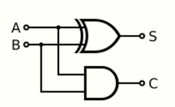
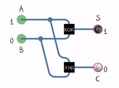
The half adder adds two single binary digits A and B. It has two outputs, sum (S) and carry (C). The carry signal represents an overflow into the next digit of a multi-digit addition. The value of the sum is 2C + S. The simplest half-adder design, pictured on the right, incorporates an XOR gate for S and an AND gate for C. The Boolean logic for the sum (in this case S) will be A′B + AB′ whereas for the carry (C) will be AB. With the addition of an OR gate to combine their carry outputs, two half adders can be combined to make a full adder.[1] The half adder adds two input bits and generates a carry and sum, which are the two outputs of a half adder. The input variables of a half adder are called the augend and addend bits. The output variables are the sum and carry. The truth table for the half adder is:
-
Inputs Outputs A B C S 0 0 0 0 0 1 0 1 1 0 0 1 1 1 1 0
1.2. Full Adder
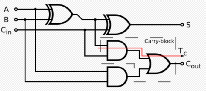
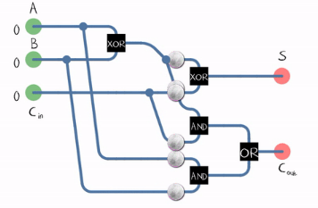
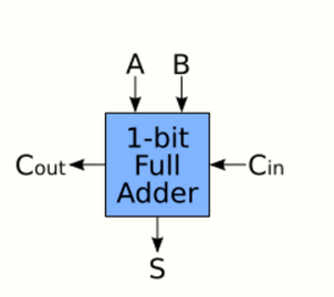
A full adder adds binary numbers and accounts for values carried in as well as out. A one-bit full-adder adds three one-bit numbers, often written as A, B, and Cin; A and B are the operands, and Cin is a bit carried in from the previous less-significant stage.[2] The full adder is usually a component in a cascade of adders, which add 8, 16, 32, etc. bit binary numbers. The circuit produces a two-bit output. Output carry and sum typically represented by the signals Cout and S, where the sum equals 2Cout + S.
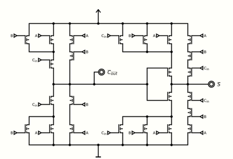
A full adder can be implemented in many different ways such as with a custom transistor-level circuit or composed of other gates. One example implementation is with S = A ⊕ B ⊕ Cin and Cout = (A ⋅ B) + (Cin ⋅ (A ⊕ B)).
In this implementation, the final OR gate before the carry-out output may be replaced by an XOR gate without altering the resulting logic. This is beacause when A and B are both 1, the term (A ⊕ B) is always 0, and hence (Cin ⋅ (A ⊕ B)) can only be 0. Thus, the inputs to the final OR gate can never be both 1's (this is the only combination for which the OR and XOR outputs differ).
Using only two types of gates is convenient if the circuit is being implemented using simple integrated circuit chips which contain only one gate type per chip.
A full adder can also be constructed from two half adders by connecting A and B to the input of one half adder, then taking its sum-output S as one of the inputs to the second half adder and Cin as its other input, and finally the carry outputs from the two half-adders are connected to an OR gate. The sum-output from the second half adder is the final sum output (S) of the full adder and the output from the OR gate is the final carry output (Cout). The critical path of a full adder runs through both XOR gates and ends at the sum bit s. Assumed that an XOR gate takes 1 delays to complete, the delay imposed by the critical path of a full adder is equal to
- [math]\displaystyle{ T_\text{FA} = 2 \cdot T_\text{XOR} = 2 D. }[/math]
The critical path of a carry runs through one XOR gate in adder and through 2 gates (AND and OR) in carry-block and therefore, if AND or OR gates take 1 delay to complete, has a delay of
- [math]\displaystyle{ T_\text{c} = T_\text{XOR} + T_\text{AND} + T_\text{OR} = D + D + D = 3D. }[/math]
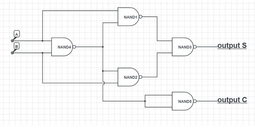
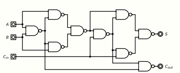
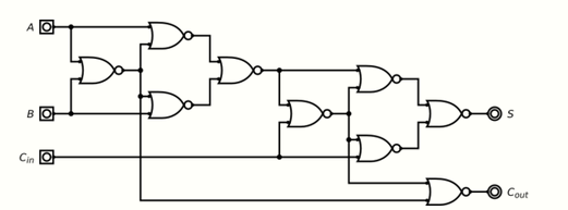
A full adder can be implemented using nine NAND gates.[3]
The truth table for the full adder is:
-
Inputs Outputs A B Cin Cout S 0 0 0 0 0 0 0 1 0 1 0 1 0 0 1 0 1 1 1 0 1 0 0 0 1 1 0 1 1 0 1 1 0 1 0 1 1 1 1 1
Inverting all inputs of a full adder also inverts all of its outputs, which can be used in the design of fast ripple-carry adders, because there is no need to invert the carry.[4]
1.3. Adders Supporting Multiple Bits
Ripple-carry adder
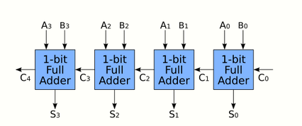
It is possible to create a logical circuit using multiple full adders to add N-bit numbers. Each full adder inputs a Cin, which is the Cout of the previous adder. This kind of adder is called a ripple-carry adder (RCA), since each carry bit "ripples" to the next full adder. Note that the first (and only the first) full adder may be replaced by a half adder (under the assumption that Cin = 0). The output of previous adder (Cout n-1)passed as input to next adder (Cin) .
The layout of a ripple-carry adder is simple, which allows fast design time; however, the ripple-carry adder is relatively slow, since each full adder must wait for the carry bit to be calculated from the previous full adder. The gate delay can easily be calculated by inspection of the full adder circuit. Each full adder requires three levels of logic. In a 32-bit ripple-carry adder, there are 32 full adders, so the critical path (worst case) delay is 3 (from input to carry in first adder) + 31 × 2 (for carry propagation in latter adders) = 65 gate delays.[5] The general equation for the worst-case delay for a n-bit carry-ripple adder, accounting for both the sum and carry bits, is
- [math]\displaystyle{ T_\text{CRA}(n) = T_\text{HA} + (n-1) \cdot T_\text{c} + T_\text{s} = T_\text{FA} + (n-1) \cdot T_c = 3 D + (n-1) \cdot 2 D = (2n+1) \cdot D. }[/math]
A design with alternating carry polarities and optimized AND-OR-Invert gates can be about twice as fast.[4][6]
Carry-lookahead adder
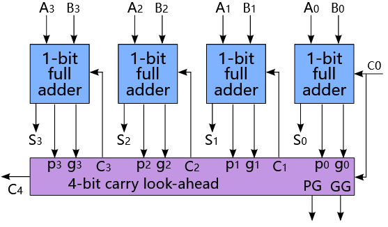
To reduce the computation time, engineers devised faster ways to add two binary numbers by using carry-lookahead adders (CLA). They work by creating two signals (P and G) for each bit position, based on whether a carry is propagated through from a less significant bit position (at least one input is a 1), generated in that bit position (both inputs are 1), or killed in that bit position (both inputs are 0). In most cases, P is simply the sum output of a half adder and G is the carry output of the same adder. After P and G are generated, the carries for every bit position are created. Some advanced carry-lookahead architectures are the Manchester carry chain, Brent–Kung adder (BKA),[7] and the Kogge–Stone adder (KSA).[8][9]
Some other multi-bit adder architectures break the adder into blocks. It is possible to vary the length of these blocks based on the propagation delay of the circuits to optimize computation time. These block based adders include the carry-skip (or carry-bypass) adder which will determine P and G values for each block rather than each bit, and the carry-select adder which pre-generates the sum and carry values for either possible carry input (0 or 1) to the block, using multiplexers to select the appropriate result when the carry bit is known.
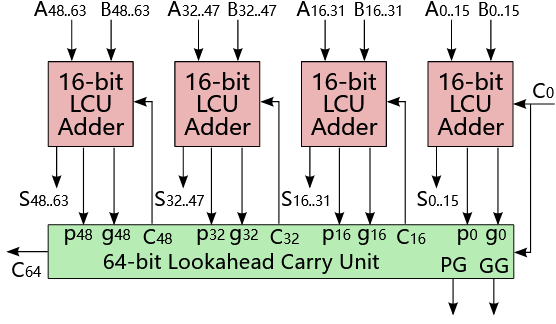
By combining multiple carry-lookahead adders, even larger adders can be created. This can be used at multiple levels to make even larger adders. For example, the following adder is a 64-bit adder that uses four 16-bit CLAs with two levels of lookahead carry units.
Other adder designs include the carry-select adder, conditional sum adder, carry-skip adder, and carry-complete adder.
Carry-save adders
If an adding circuit is to compute the sum of three or more numbers, it can be advantageous to not propagate the carry result. Instead, three-input adders are used, generating two results: a sum and a carry. The sum and the carry may be fed into two inputs of the subsequent 3-number adder without having to wait for propagation of a carry signal. After all stages of addition, however, a conventional adder (such as the ripple-carry or the lookahead) must be used to combine the final sum and carry results.
1.4. 3:2 Compressors
A full adder can be viewed as a 3:2 lossy compressor: it sums three one-bit inputs and returns the result as a single two-bit number; that is, it maps 8 input values to 4 output values. Thus, for example, a binary input of 101 results in an output of 1 + 0 + 1 = 10 (decimal number 2). The carry-out represents bit one of the result, while the sum represents bit zero. Likewise, a half adder can be used as a 2:2 lossy compressor, compressing four possible inputs into three possible outputs.
Such compressors can be used to speed up the summation of three or more addends. If the addends are exactly three, the layout is known as the carry-save adder. If the addends are four or more, more than one layer of compressors is necessary, and there are various possible designs for the circuit: the most common are Dadda and Wallace trees. This kind of circuit is most notably used in multipliers, which is why these circuits are also known as Dadda and Wallace multipliers.
2. Quantum Adders
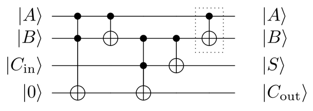
Using only the Toffoli and CNOT quantum logic gates, it is possible to produce quantum full- and half-adders.[10][11][12] The same circuits can also be implemented in classical reversible computation, as both CNOT and Toffoli are also classical logic gates.
Since the quantum Fourier transform have a low circuit complexity, it can efficiently be used for adding numbers as well.[13][14]
3. Analog Adders
Just as in Binary adders, combining two input currents effectively adds those currents together. Within the constraints of the hardware, non-binary signals (i.e. with a base higher than 2) can be added together to calculate a sum. Also known as a "summing amplifier",[15] this technique can be used to reduce the number of transistors in an addition circuit.
References
- Excel HSC Software Design and Development. Pascal Press. 2004. p. 180. ISBN 978-1-74125175-3. https://books.google.com/books?id=PZkDpS4m0fMC&pg=PA180.
- Digital Logic and Computer Design. Prentice-Hall. 1979. pp. 119–123. ISBN 978-0-13-214510-7. https://archive.org/details/digitallogiccomp00mano/page/119.
- Half Adder and Full Adder Circuits, 2021-04-15, https://www.electronicshub.org/half-adder-and-full-adder-circuits/#Full_Adder_using_NAND_Gates, retrieved 2021-07-27
- Fischer, P.. "Einfache Schaltungsblöcke". Universität Heidelberg. https://sus.ziti.uni-heidelberg.de/Lehre/WS1617_DST/DST_Fischer_06_Einfache_Bloecke_FF.pptx.pdf. Retrieved 2021-09-05.
- Design and Implementation of Carry Select Adder Using T-Spice. Anchor Academic Publishing. 2016. p. 22. ISBN 978-3-96067058-2. https://books.google.com/books?id=F_AWDQAAQBAJ&pg=PA22.
- "Fast Ripple-Carry Adders in Standard-Cell CMOS VLSI". 20th IEEE Symposium on Computer Arithmetic. 2011. pp. 103–111. http://ieeexplore.ieee.org/Xplore/login.jsp?url=http%3A%2F%2Fieeexplore.ieee.org%2Fiel5%2F5991607%2F5992089%2F05992115.pdf%3Farnumber%3D5992115&authDecision=-203.
- "A Regular Layout for Parallel Adders". IEEE Transactions on Computers C-31 (3): 260–264. March 1982. doi:10.1109/TC.1982.1675982. ISSN 0018-9340. http://www.dtic.mil/get-tr-doc/pdf?AD=ADA074455.
- "A Parallel Algorithm for the Efficient Solution of a General Class of Recurrence Equations". IEEE Transactions on Computers C-22 (8): 786–793. August 1973. doi:10.1109/TC.1973.5009159. https://dx.doi.org/10.1109%2FTC.1973.5009159
- Reynders, Nele; Dehaene, Wim (2015). Ultra-Low-Voltage Design of Energy-Efficient Digital Circuits. Analog Circuits And Signal Processing (ACSP) (1 ed.). Cham, Switzerland: Springer International Publishing AG Switzerland. doi:10.1007/978-3-319-16136-5. ISBN 978-3-319-16135-8. https://dx.doi.org/10.1007%2F978-3-319-16136-5
- Feynman, Richard P. (1986). "Quantum mechanical computers". Foundations of Physics (Springer Science and Business Media LLC) 16 (6): 507–531. doi:10.1007/bf01886518. ISSN 0015-9018. Bibcode: 1986FoPh...16..507F. https://dx.doi.org/10.1007%2Fbf01886518
- "Code example: Quantum full adder". QuTech (Delft University of Technology (TU Delft) and the Netherlands Organisation for Applied Scientific Research (TNO)). https://www.quantum-inspire.com/kbase/full-adder/.
- Dibyendu Chatterjee, Arijit Roy (2015). "A transmon-based quantum half-adder scheme". Progress of Theoretical and Experimental Physics 2015 (9). doi:10.1093/ptep/ptv122. Bibcode: 2015PTEP.2015i3A02C. https://paperity.org/p/73955611/a-transmon-based-quantum-half-adder-scheme.
- Draper, Thomas G. (7 Aug 2000). "Addition on a Quantum Computer". arXiv:quant-ph/0008033. //arxiv.org/abs/quant-ph/0008033
- Ruiz-Perez, Lidia; Juan Carlos, Garcia-Escartin (2 May 2017). "Quantum arithmetic with the quantum Fourier transform". Quantum Information Processing 16 (6): 152. doi:10.1007/s11128-017-1603-1. Bibcode: 2017QuIP...16..152R. https://dx.doi.org/10.1007%2Fs11128-017-1603-1
- "Summing Amplifier is an Op-amp Voltage Adder". 22 August 2013. https://www.electronics-tutorials.ws/opamp/opamp_4.html.