 +1 credit
| Version | Summary | Created by | Modification | Content Size | Created at | Operation |
|---|---|---|---|---|---|---|
| 1 | Yanglizhi Li | + 3544 word(s) | 3544 | 2020-12-07 14:11:49 | | | |
| 2 | Peter Tang | -47 word(s) | 3497 | 2020-12-19 13:46:14 | | |
Video Upload Options
Chemical vapor deposition is the most promising technique for the mass production of high-quality graphene, in which the metal substrate plays a crucial role in the catalytic decomposition of the carbon source, assisting the attachment of the active carbon species, and regulating the structure of the graphene film. Due to some drawbacks of single metal substrates, alloy substrates have gradually attracted attention owing to their complementarity in the catalytic growth of graphene.
1. Introduction
The rise of graphene [1][2] has aroused a new upsurge in exploring its intriguing physical and chemical properties on a two-dimensional scale [3][4][5][6][7][8][9], as well as its unique applications superior to those of bulk materials [10][11][12][13]. As an essential prerequisite for both fundamental research and practical utilization, the facile, cost-effective, and well-controlled preparation of graphene films with desired structures and properties has indubitably become the pursuit of academia. After more than a decade of research, chemical vapor deposition (CVD), and in particular CVD based on the use of metal catalysts, has stood out owing to its considerable advantages in the mass production of high-quality graphene films, thereby paving the way for its commercialization [14][15][16].
During the CVD growth of graphene films, the metal substrates, which catalyze the decomposition of the carbon sources into active carbon species and the subsequent assembly of these species into graphene, play vital roles in regulating the structure and properties of the resulting film. In general, single metal catalysts can be divided into two categories. The first is represented by a metal with a low carbon solubility, such as Cu, which features the self-limited model for growth of monolayer graphene but suffers from a relatively low catalytic activity [17]. The second category is represented by Ni, which has a high carbon solubility and catalytic activity, and the segregation of inhomogeneous multilayer graphene is a common phenomenon [18]. With the rapid development of market demand and downstream applications, higher requirements have been put forward for the efficient preparation of graphene for specific demands. For instance, precise layer number control during the CVD process is of significant interest because the properties of graphene drastically change with the number of layers and their respective stacking orders. More specifically, the well-known tunable bandgap [19], the twisted-angle-dependent van Hove singularities [20][21], and unconventional superconductivity [22][23] only exist in bilayer graphene (BLG) with specific stacking structures. Moreover, the process of commercialization requires the rapid and low-temperature preparation of single-crystal graphene films [24][25]. In this regard, alloy metal substrates, such as Cu/Ni [26], Ni/Mo [27], Cu/Si [28], Pt/Si [29], Ni/Au [30], Ni/Ti [31], and Cu/Co [32], which combine the advantages of the different metal components, provide more significant benefits than single metal catalysts in terms of bridging the aforementioned gap. Therefore, the rational design of alloy catalysts is leading to a new trend in the controlled growth of high-quality graphene materials [33].
2. Elementary Steps for Graphene Growth on Metal Catalysts
Generally, a complete graphene preparation process includes the following steps: (1) pretreatment of the metal substrates (such as polishing and coating); (2) heating and annealing to enable grain coarsening, surface reconstruction, or/and complete alloying of the metal substrates; (3) graphene growth (at ~1000 °C in most cases); (4) cooling stages that are closely related to the segregation and wrinkling phenomenon of graphene. Specifically, several refined elementary steps exist during the graphene growth stage. For example, the carbon sources undergo a partial gas-phase reaction and mass transport in the chamber of the CVD system, followed by adsorption and stepwise decomposition into active carbon species on the surface of the metal catalyst [34]. Subsequently, two possible destinations are available for the carbon species depending on the carbon solubility and the metal–carbon interactions. One is on-surface migration, together with subsequent nucleation and edge-attachment to realize surface-mediated graphene growth, as is usually observed on metals with a low carbon solubility [17]. The second is dissolution into bulk metals with a high carbon solubility at high temperatures, and segregation to form graphene during the cooling stages due to the decreased carbon solubility [35] (Figure 1). Following the selection of an appropriate metal substrate, the growth mode is also assigned, leaving a limited growth window for regulating the structures of CVD-grown graphene. For instance, the self-limited growth mode of graphene on Cu renders it a promising substrate for the growth of single-layer graphene films. However, the low carbon solubility hinders the formation of large-area uniform bilayer or multilayer graphene, and the relatively weak catalytic activity [36] usually leads to a low growth rate.
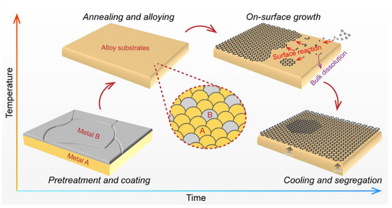
Figure 1. Process flow and elementary steps for graphene growth on metal substrates.
Fortunately, owing to the mutual solubility of many transitional metals, alloy substrates, which possess the combined advantages of multiple metal components, provide significantly more possibilities for the controllable growth of graphene upon adjusting the composition and proportion of each metal element. This is manifested in, but not limited to, the following aspects: (1) the catalytic activity of the catalyst can be enhanced to increase the growth rate of graphene by alloying a certain proportion of the metal with a high catalytic activity into the original single metal matrix; (2) the carbon solubility can be tuned for the layer number control of graphene films by carefully designing the proportion of each metal component; (3) the metal–graphene interaction could be modified by varying the surface state of the metals after alloying. Therefore, the selection of metal elements and their relative contents are crucial in the design of binary alloy catalysts.
Generally speaking, there are two sources of the metals that make up alloy catalysts. One source includes the commonly used transition metals, including those with low carbon solubilities and/or weak metal–graphene interactions, such as Cu [17], Au [37], and Pt [38], in addition to those with high carbon solubilities and strong metal–graphene interactions, such as Ni [18] and Co [39], and those forming strong bonds with carbon, such as Ti [40][41] and Mo [42]. Another source is some nonmetallic elements that can form alloys with metals, such as Si. As mentioned above, the catalytic activity, carbon solubility, and interface interaction should be comprehensively considered to determine the elements present in an alloy (Figure 2). In addition, the miscibility of the elements is also an important prerequisite for the formation of alloys. Some physical properties of representative metals and Si crystals are listed in Table 1 for reference.
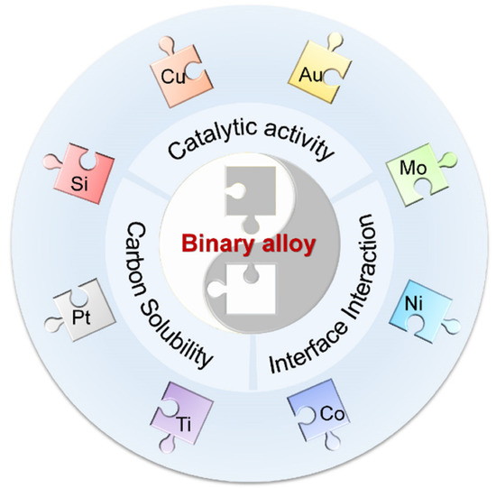
Figure 2. Rational design of binary alloy catalysts in terms of the catalytic activity, carbon solubility, and metal–graphene interactions.
Table 1. Summary of the physical properties of representative metals and Si crystals.
|
Metal |
Au |
Co |
Cu |
Mo |
Ni |
Pt |
Si |
Ti |
|
Carbon solubility (at.%, 1000 °C) 1 |
0.01 |
3.41 |
0.04 |
0.50 |
1.3 |
1.76 |
- |
1.88 |
|
Lattice constant (Å) 2 |
4.0786 |
3.5442 |
3.6150 |
3.1653 |
3.5238 |
3.9231 |
5.4305 |
a = b = 2.953 c = 4.729 |
|
Melting point (°C) 2 |
1064.18 |
1495 |
1084.62 |
2623 |
1455 |
1768.4 |
1414 |
1668 |
|
Metal–graphene interaction 3 |
π = intact |
- |
π = intact |
- |
π = 2 eV |
π = intact |
- |
- |
|
Electron configurations 4 |
5d106s1 |
3d74s2 |
3d104s1 |
4d55s1 |
3d84s2 |
5d96s1 |
3s23p2 |
3d24S2 |
1 The carbon solubility values were obtained from Ref [43]. 2 The lattice constant and melting point values were obtained from Ref [44]. 3 The metal–graphene interactions were measured by the amount of downward shift of the π-band of graphene on the metal. “Intact” means a weak metal–graphene interaction (i.e., a linear dispersion at the Dirac point is still intact). These values were obtained from Ref [45]. 4 The catalytic activity is strongly influenced by the electron configuration. For instance, due to the absence of empty d orbitals, Cu has a low catalytic activity.
3. Layer Number Control of the Graphene Films
Monolayer graphene exhibits an ultrahigh carrier mobility, thermal conductivity, and mechanical strength; however, the lack of a band gap impedes its application in logic circuits [46]. One promising solution to open the band gap is the use of AB-stacked BLG, whose bandgap can be tuned using an external electric field [19]. In addition, exploration of the novel physical properties of twisted BLG is also in its initial stages [47][48]. Consequently, precise control of the layer number and stacking orders of CVD-grown graphene films is of great significance.
To control the layer number, one promising strategy is the use of the segregation technique proposed by Liu's group, where the as-formed graphene film originates from the carbon atoms dissolved in the bulk of the catalysts [35]. Therefore, binary alloys with adjustable carbon solubilities would be preferred, as in the case of the Cu/Ni alloy. More specifically, through the deposition of metal films (e.g., Ni and Cu) on SiO2/Si substrates to form a sandwiched Cu/Ni/SiO2/Si structure and subsequent high-temperature annealing, a Cu/Ni alloy can be formed, accompanied by the segregation of graphene films from the dissolved carbon atoms (Figure 3a). The plausible kinetic processes are summarized as follows. The dissolved carbon atoms undergo dynamic diffusion in the bulk, with some of them escaping onto the surface of the metal to initiate surface-mediated diffusion. Subsequently, the graphene domains nucleate at the defect or stepped sites of the catalysts and expand their size during the growth stage (Figure 3b). Indeed, this was the first time that the Cu/Ni alloy was used as the catalyst to prepare uniform graphene films (Figure 3c). The possibility of controlling the layer number of graphene films by the segregation technique was also explored, since this benefits from the fact that the atomic percentage of Ni can be precisely defined by controlling the thickness of the Ni films during the deposition process [26]. As shown in Figure 3d–k, a uniform monolayer graphene film with 95% coverage and BLG with 89% coverage were achieved by increasing the Ni content from 5.5 and 10.4%, respectively. A further increase in the Ni content gave rise to thicker graphene films. For the case of a low Ni content, the segregation behavior is approximately determined by Cu, where the weak metal–graphene interactions and low carbon solubility weaken the influence from the substrate, and result in the formation of single-layer graphene. The increase in the Ni content leads to the dissolution of a greater number of carbon atoms in the alloys to ultimately yield increased layer numbers of graphene.
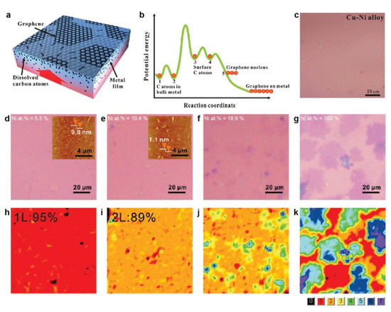
Figure 3. Segregation growth of graphene films on Cu/Ni alloy catalysts. (a) Schematic illustration of the segregation method to prepare the graphene films. (b) Energy profiles of the carbon atoms during the segregation process. (c) Optical image of the graphene film on SiO2/Si grown using a Cu/Ni alloy catalyst. (a–c) Reprinted with permission from [35]. Copyright (2011), American Chemical Society. (d–g) Optical images of the graphene films grown from Cu/Ni alloy substrates with Ni atomic percentages of (d) 5.5%, (e) 10.4%, (f) 18.9%, and (g) 100%. The insets in (d,e) represent the corresponding atomic force microscopy images. (h–k) Layer number distributions obtained from the optical contrasts corresponding to (d–g), respectively. (d–k) Reprinted with permission from [26]. Copyright (2011), American Chemical Society.
Commercial polycrystalline Cu/Ni foils have also been employed to prepare graphene films with different layer distributions by regulating the growth temperature and cooling rate [49]. It was found that upon increasing the growth temperature from 930 to 1030 °C with a cooling rate of 100 °C/s, the layer numbers of graphene varied from the sub monolayer to 2–5 layers owing to the increased carbon solubility of the Cu/Ni substrates. Moreover, the cooling rate had a significant influence on determining the layer number of graphene. More specifically, lowering the cooling rate to 5 °C/s resulted in the formation of significantly thicker graphene films, which is in stark contrast with the case operating at a faster cooling rate. Furthermore, the growth mechanism of graphene grown on the Cu/Ni alloy was revealed by isotope labeling [50]. Through the sequential introduction of 12CH4 and 13CH4 during the graphene growth process, BLG composed of the randomly mixed 12C and 13C was obtained on the surface of the Cu90Ni10 substrates, indicating that the surface precipitation mechanism dominated the Cu/Ni alloy. The influence of the nickel content and growth parameters on the number of graphene layers was investigated in detail at a later date [51][52][53].
In addition to the pursuit of the layer control, the preparation of BLG films with specific stacking sequences, such as AB-stacking BLG, has also attracted much attention. In 2014, Liu et al. achieved large uniform AB-stacking bilayer graphene (>98%) films on a Cu75Ni25 alloy through careful optimization of the surface carbon concentration [54]. The higher abundance of Cu on the surface compared to that in the bulk is considered to be a critical factor in decreasing the carbon diffusion in the bulk to enable the uniform growth of BLG. Later, in 2016, the Cu-vapor-assisted method was invented to reduce the effective content of Ni on the surface of the Cu/Ni alloy [55], thus further decreasing the on-surface growth rate of the first layer to enable more carbon diffusion into the catalyst. As a result, the second layer can segregate with a large coverage (>90%) to form AB-stacking BLG.
The crystal orientation of the Cu/Ni substrates was identified as another key factor in determining the stacking order of BLG by Ago's group [56]. In their work, a c-plane sapphire wafer was used as the epitaxial template for preparing Cu80/Ni20(111) films. Subsequently, BLG films were formed in two consecutive processes: the first layer of graphene was formed in the high-temperature stage following the surface growth mode, while the second layer segregated from the bulk during the cooling stage. Through careful characterization, four typical stacking configurations of the as-prepared BLG film with respect to the substrate were identified, namely aligned/aligned, 30°-rotated/aligned, 30°-rotated/30°-rotated, and aligned/30°-rotated configuration (Figure 4a), among which the proportion of the AB-stacking BLG accounted for 70–80%. According to density functional theory calculations, the graphene domains on the Cu/Ni(111) substrates possess a dominant orientation (0°) and a metastable orientation (30°), which explains the existence of the 30°-rotated configuration. Therefore, further exploration of the preparation of perfect AB-stacking BLG films is necessary. Recently, with the significant advances in the preparation of single-crystal Cu foils [57][58][59], single-crystal Cu/Ni(111) foils can be obtained by Ni plating on Cu foil and subsequent annealing [60] (Figure 4c,d). On the basis of the single-crystal catalysts that prevent non-uniform segregation at the grain boundary, uniform BLG films (>95% coverage and almost 100% AB-stacking configurations) and trilayer graphene (TLG) films (>60% coverage and almost 100% ABA-stacking configurations) were segregated from the Cu/Ni alloy, where the layer number control was found to depend strongly on the precise adjustment of the Ni content (Figure 4e–g).
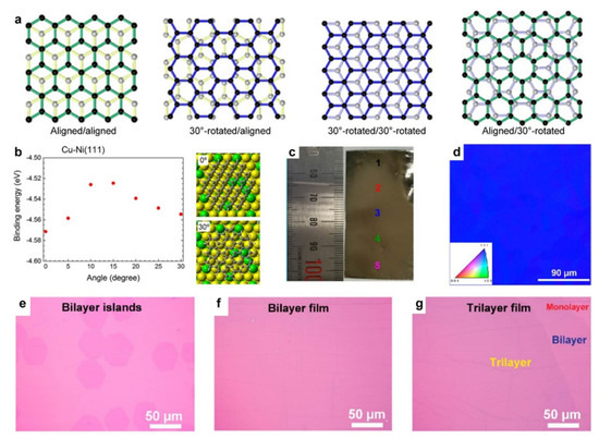
Figure 4. Growth of AB-stacking bilayer graphene (BLG) on Cu/Ni alloy catalysts. (a) Schematic illustration of the typical stacking orientations of BLG with respect to that of the substrate. (b) The binding energy of graphene on Cu/Ni(111) as a function of the relative orientation. (a,b) Reprinted with permission from [56]. Copyright (2016), American Chemical Society. (c) Photographic image of the Cu/Ni(111) foil. (d) EBSD IPF image of the Cu/Ni(111) foil. (e–g) Optical images of (e) the BLG islands, (f) a continuous BLG film, and (g) a TLG film. (c–g) Reprinted with permission from [60]. Copyright (2020), Springer Nature.
In addition to Cu/Ni substrates, some other alloy systems, such as Cu/Co, Pt/Si, and Cu/Si, are also strong candidates for controlling the layer number and/or stacking configurations of graphene. For instance, similar to Ni, Co has a moderate carbon solubility and partakes in strong interactions with graphene, and so can be integrated into the alloy catalyst. Lin et al. deposited Co films on the top of Cu foil to form the Co/Cu composite as the catalyst to control the layer number of the graphene film, where the Co film served as the carbon capture layer while the inter-diffusion of Cu atoms into the Co layer regulated the carbon solubility of the Co layer [32].
Although extensive efforts have been made, several challenges still exist. For example, because the interlayer coupling between two layers of graphene is not sufficiently strong to prevent the influence of substrates with a non-uniform surface state, obtaining a continuous perfect AB-stacking BLG film remains a challenge. To address this issue, novel Pt3Si/Pt substrates were utilized as catalysts [61]. As shown in Figure 5a, a core–shell structure is clearly distinguished after the deposition of a Si film on polycrystalline Pt foils followed by high-temperature annealing. Given that the Pt core features a high melting point (1768.4 °C), while the Pt3Si shell melts at a relatively low temperature (830 °C), it tends to form a surface melting state, i.e., liquid Pt3Si, at the growth temperature of graphene (1100–1025 °C), which is crucial for the interlayer epitaxial growth of uniform AB-stacking BLG. Following the on-surface growth of the first layer of graphene at 1100 °C (Figure 5b), the liquid Pt3Si provides a channel for carbon atoms precipitating from the Pt core to the surface. As a consequence, uniform BLG films were formed (Figure 5c). In addition, the smooth and uniform surface of the liquid Pt3Si renders the graphene domains easier to rotate on the liquid surface, allowing them to adopt the energy-favorable AB-stacking configuration (Figure 5d). These together contribute to the formation of a large AB-stacking BLG film. Very recently, significant progress has been made in synthesizing extremely uniform (100%) AB-stacking BLG and ABA-stacking TLG on a Cu/Si alloy [28]. Overall, four steps are involved in the preparation of graphene films: (1) The Cu/Si alloy is formed by annealing the Cu(111) film inside the quartz chamber at 900 °C, where the Si atoms come from the quartz tube; (2) the SiC layer is formed on the surface of the catalyst by introducing a carbon source (CH4) into the chamber; (3) as the temperature increases to 1075 °C, graphene domains nucleate owing to the sublimation of Si atoms from the SiC layer; (4) the graphene domains expand with elongation of the annealing time, and finally merge into full graphene films (Figure 5e). Contrary to the segregation phenomenon on the Cu/Ni alloy, once the layer number of the initial graphene nuclei on the Cu/Si alloy is determined, each layer grows simultaneously at the same rate throughout the growth process, which is attributed to the diffusion-to-sublimation growth mode (Figure 5f). It was found that the layer numbers of graphene films can be precisely controlled by tuning the CH4 concentrations during the process of SiC formation. Moreover, an optimal Si content (28.7%) exists in Cu/Si alloy catalysts to ensure the uniformity of the graphene layer, in which a small Si content will lead to a non-uniform thickness of the graphene films, while a larger Si content results in insufficient graphene growth due to the limited catalytic activity for decomposing the carbon source.
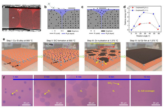
Figure 5. Growth of graphene films with well-controlled layer numbers on catalysts other than Cu/Ni. (a) Cross-section scanning electron microscopy (SEM) image and energy dispersive spectroscopy mapping of the Pt3Si/Pt foils. (b,c) Schematic illustration of uniform multilayer growth of (b) the first and (c) the second layer of graphene on a Pt3Si/Pt substrate. (d) The relative energies of graphene on Pt and Pt3Si as a function of the relative orientations. (a–d) Reprinted with permission from [61]. Copyright (2019), Springer Nature. (e) Schematic illustration of the uniform multilayer graphene films grown on the Cu/Si alloy catalyst. (f) Optical images of the time evolution of tetralayer graphene (Si/SiO2 substrates) grown from the Cu/Si alloy. (e,f) Reprinted with permission from [28]. Copyright (2020), Springer Nature.
The aforementioned works focus on the controllable growth of bilayer or multilayer graphene with tunable carbon solubility on complementary alloy substrates. At the same time, the synthesis of absolute monolayer graphene within a wide growth window is also promising. Even on a Cu surface, strict monolayer graphene is not easy to acquire [62]. Given that the non-uniform multilayer graphene originates from non-equilibrium precipitation in metals with a high carbon solubility, such as Ni [63], the Mo component, which has a strong tendency to form molybdenum carbides (MoC) with carbon, was added into the Ni matrix to absorb the excess carbon dissolved in the bulk [27]. As shown in Figure 6a, the carbon atoms decomposed from the carbon source can either recombine into monolayer graphene on the Ni/Mo surface or diffuse into the bulk, where the latter route is not reversible because the carbon atoms are fixed in the bulk in the form of MoC. As a consequence, strict monolayer graphene films were realized as confirmed by transmission electron microscopy (TEM) and atomic force microscopy (AFM) characterizations (Figure 6b,c). The most fascinating advantage of growing monolayer graphene on a Ni/Mo alloy is its high tolerance to a wide range of growth parameters, including the growth time, C/H ratio in the carbon source, Ni/Mo ratio in the alloy, growth temperature, and cooling rate (Figure 6d). In addition to the Ni/Mo alloy, the Co/Mo alloy also shows similar properties.
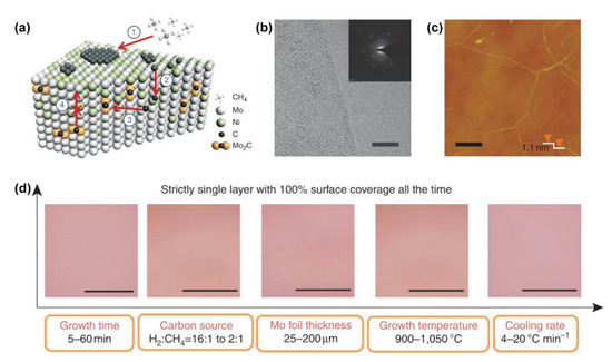
Figure 6. Growth of strict monolayer graphene on a Ni/Mo alloy. (a) Schematic illustration of the growth mechanism of graphene on a Ni/Mo alloy. (b) TEM and (c) AFM images of the monolayer graphene grown on a Ni/Mo alloy. Inset in (b) is the corresponding selected area electron diffraction pattern. (d) Optical images of the strict monolayer graphene synthesized using different growth parameters. Reprinted with permission from [27]. Copyright (2011), Springer Nature.
References
- Novoselov, K.S.; Geim, A.K.; Morozov, S.V.; Jiang, D.; Zhang, Y.; Dubonos, S.V.; Grigorieva, I.V.; Firsov, A.A. Electric field effect in atomically thin carbon films. Science 2004, 306, 666–669.
- Geim, A.K.; Novoselov, K.S. The rise of graphene. Nat. Mater. 2007, 6, 183–191.
- Nair, R.R.; Blake, P.; Grigorenko, A.N.; Novoselov, K.S.; Booth, T.J.; Stauber, T.; Peres, N.M.R.; Geim, A.K. Fine structure constant defines visual transparency of graphene. Science 2008, 320, 1308.
- Novoselov, K.S.; Jiang, Z.; Zhang, Y.; Morozov, S.V.; Stormer, H.L.; Zeitler, U.; Maan, J.C.; Boebinger, G.S.; Kim, P.; Geim, A.K. Room-temperature quantum hall effect in graphene. Science 2007, 315, 1379.
- Novoselov, K.S.; Geim, A.K.; Morozov, S.V.; Jiang, D.; Katsnelson, M.I.; Grigorieva, I.V.; Dubonos, S.V.; Firsov, A.A. Two-dimensional gas of massless Dirac fermions in graphene. Nature 2005, 438, 197–200.
- Du, X.; Skachko, I.; Duerr, F.; Luican, A.; Andrei, E.Y. Fractional quantum Hall effect and insulating phase of Dirac electrons in graphene. Nature 2009, 462, 192–195.
- Bolotin, K.I.; Ghahari, F.; Shulman, M.D.; Stormer, H.L.; Kim, P. Observation of the fractional quantum Hall effect in graphene. Nature 2009, 462, 196–199.
- Lee, C.; Wei, X.; Kysar, J.W.; Hone, J. Measurement of the elastic properties and intrinsic strength of monolayer graphene. Science 2008, 321, 385–388.
- Balandin, A.A.; Ghosh, S.; Bao, W.; Calizo, I.; Teweldebrhan, D.; Miao, F.; Lau, C.N. Superior thermal conductivity of single-layer graphene. Nano Lett. 2008, 8, 902–907.
- Bae, S.; Kim, H.; Lee, Y.; Xu, X.; Park, J.-S.; Zheng, Y.; Balakrishnan, J.; Lei, T.; Ri Kim, H.; Song, Y.I.; et al. Roll-to-roll production of 30-inch graphene films for transparent electrodes. Nat. Nanotechnol. 2010, 5, 574–578.
- Schwierz, F. Graphene transistors. Nat. Nanotechnol. 2010, 5, 487–496.
- Kim, K.; Choi, J.-Y.; Kim, T.; Cho, S.-H.; Chung, H.-J. A role for graphene in silicon-based semiconductor devices. Nature 2011, 479, 338–344.
- Koppens, F.H.L.; Mueller, T.; Avouris, P.; Ferrari, A.C.; Vitiello, M.S.; Polini, M. Photodetectors based on graphene, other two-dimensional materials and hybrid systems. Nat. Nanotechnol. 2014, 9, 780–793.
- Lin, L.; Deng, B.; Sun, J.; Peng, H.; Liu, Z. Bridging the gap between reality and ideal in chemical vapor deposition growth of graphene. Chem. Rev. 2018, 118, 9281–9343.
- Yang, J. Towards large-scale and high-quality graphene films. Acta Phys. Chim. Sin. 2019, 35, 1043–1044.
- Lin, L.; Peng, H.; Liu, Z. Synthesis challenges for graphene industry. Nat. Mater. 2019, 18, 520–524.
- Li, X.; Cai, W.; An, J.; Kim, S.; Nah, J.; Yang, D.; Piner, R.; Velamakanni, A.; Jung, I.; Tutuc, E.; et al. Large-area synthesis of high-quality and uniform graphene films on copper foils. Science 2009, 324, 1312–1314.
- Reina, A.; Jia, X.; Ho, J.; Nezich, D.; Son, H.; Bulovic, V.; Dresselhaus, M.S.; Kong, J. Large area, few-layer graphene films on arbitrary substrates by chemical vapor deposition. Nano Lett. 2009, 9, 30–35.
- Zhang, Y.; Tang, T.-T.; Girit, C.; Hao, Z.; Martin, M.C.; Zettl, A.; Crommie, M.F.; Shen, Y.R.; Wang, F. Direct observation of a widely tunable bandgap in bilayer graphene. Nature 2009, 459, 820–823.
- Li, G.; Luican, A.; Lopes Dos Santos, J.M.B.; Castro Neto, A.H.; Reina, A.; Kong, J.; Andrei, E.Y. Observation of Van Hove singularities in twisted graphene layers. Nat. Phys. 2010, 6, 109–113.
- Yin, J.; Wang, H.; Peng, H.; Tan, Z.; Liao, L.; Lin, L.; Sun, X.; Koh, A.L.; Chen, Y.; Peng, H.; et al. Selectively enhanced photocurrent generation in twisted bilayer graphene with van Hove singularity. Nat. Commun. 2016, 7, 10699.
- Cao, Y.; Fatemi, V.; Demir, A.; Fang, S.; Tomarken, S.L.; Luo, J.Y.; Sanchez-Yamagishi, J.D.; Watanabe, K.; Taniguchi, T.; Kaxiras, E.; et al. Correlated insulator behaviour at half-filling in magic-angle graphene superlattices. Nature 2018, 556, 80–84.
- Cao, Y.; Fatemi, V.; Fang, S.; Watanabe, K.; Taniguchi, T.; Kaxiras, E.; Jarillo-Herrero, P. Unconventional superconductivity in magic-angle graphene superlattices. Nature 2018, 556, 43–50.
- Deng, B.; Xin, Z.; Xue, R.; Zhang, S.; Xu, X.; Gao, J.; Tang, J.; Qi, Y.; Wang, Y.; Zhao, Y.; et al. Scalable and ultrafast epitaxial growth of single-crystal graphene wafers for electrically tunable liquid-crystal microlens arrays. Sci. Bull. 2019, 64, 659–668.
- Zhang, X.; Wu, T.; Jiang, Q.; Wang, H.; Zhu, H.; Chen, Z.; Jiang, R.; Niu, T.; Li, Z.; Zhang, Y.; et al. Epitaxial growth of 6 in. single‐crystalline graphene on a Cu/Ni (111) Film at 750 °C via chemical vapor deposition. Small 2019, 15, 1805395.
- Liu, X.; Fu, L.; Liu, N.; Gao, T.; Zhang, Y.; Liao, L.; Liu, Z. Segregation growth of graphene on Cu-Ni alloy for precise layer control. J. Phys. Chem. C 2011, 115, 11976–11982.
- Dai, B.; Fu, L.; Zou, Z.; Wang, M.; Xu, H.; Wang, S.; Liu, Z. Rational design of a binary metal alloy for chemical vapour deposition growth of uniform single-layer graphene. Nat. Commun. 2011, 2, 522–526.
- Nguyen, V.L.; Duong, D.L.; Lee, S.H.; Avila, J.; Han, G.; Kim, Y.M.; Asensio, M.C.; Jeong, S.Y.; Lee, Y.H. Layer-controlled single-crystalline graphene film with stacking order via Cu–Si alloy formation. Nat. Nanotechnol. 2020, doi:10.1038/s41565-020-0743-0.
- Babenko, V.; Murdock, A.T.; Koós, A.A.; Britton, J.; Crossley, A.; Holdway, P.; Moffat, J.; Huang, J.; Alexander-Webber, J.A.; Nicholas, R.J.; et al. Rapid epitaxy-free graphene synthesis on silicidated polycrystalline platinum. Nat. Commun. 2015, 6, 7536.
- Weatherup, R.S.; Bayer, B.C.; Blume, R.; Ducati, C.; Baehtz, C.; Schlögl, R.; Hofmann, S. In situ characterization of alloy catalysts for Low-temperature graphene growth. Nano Lett. 2011, 11, 4154–4160.
- Li, J.; Wang, G.; Geng, H.; Zhu, H.; Zhang, M.; Di, Z.; Liu, X.; Chu, P.K.; Wang, X. CVD growth of graphene on NiTi alloy for enhanced biological activity. ACS Appl. Mater. Interfaces 2015, 7, 19876–19881.
- Lin, T.; Huang, F.; Wan, D.; Bi, H.; Xie, X.; Jiang, M. Self-regulating homogenous growth of high-quality graphene on Co-Cu composite substrate for layer control. Nanoscale 2013, 5, 5847–5853.
- Yan, K.; Fu, L.; Peng, H.; Liu, Z. Designed CVD growth of graphene via process engineering. Acc. Chem. Res. 2013, 46, 2263–2274.
- Zhang, X.; Li, H.; Ding, F. Self-Assembly of carbon atoms on transition metal surfaces-chemical vapor deposition growth mechanism of graphene. Adv. Mater. 2014, 26, 5488–5495.
- Liu, N.; Fu, L.; Dai, B.; Yan, K.; Liu, X.; Zhao, R.; Zhang, Y.; Liu, Z. Universal segregation growth approach to wafer-size graphene from non-noble metals. Nano Lett. 2011, 11, 297–303.
- Wang, X.; Yuan, Q.; Li, J.; Ding, F. The transition metal surface dependent methane decomposition in graphene chemical vapor deposition growth. Nanoscale 2017, 9, 11584–11589.
- Nie, S.; Bartelt, N.C.; Wofford, J.M.; Dubon, O.D.; McCarty, K.F.; Thürmer, K. Scanning tunneling microscopy study of graphene on Au(111): Growth mechanisms and substrate interactions. Phys. Rev. B 2012, 85, 205406–205406.
- Sutter, P.; Sadowski, J.T.; Sutter, E. Graphene on Pt(111): Growth and substrate interaction. Phys. Rev. B 2009, 80, 1–10.
- Eom, D.; Prezzi, D.; Rim, K.T.; Zhou, H.; Lefenfeld, M.; Xiao, S.; Nuckolls, C.; Hybertsen, M.S.; Heinz, T.F.; Flynn, G.W. Structure and electronic properties of graphene nanoislands on CO(0001). Nano Lett. 2009, 9, 2844–2848.
- Aizawa, T.; Souda, R.; Otani, S.; Ishizawa, Y.; Oshima, C. Bond softening in monolayer graphite formed on transition-metal carbide surfaces. Phys. Rev. B 1990, 42, 11469–11478.
- Aizawa, T.; Souda, R.; Otani, S.; Ishizawa, Y.; Oshima, C. Anomalous bond of monolayer graphite on transition-metal carbide surfaces. Phys. Rev. Lett. 1990, 64, 768–771.
- Wu, Y.; Yu, G.; Wang, H.; Wang, B.; Chen, Z.; Zhang, Y.; Wang, B.; Shi, X.; Xie, X.; Jin, Z.; et al. Synthesis of large-area graphene on molybdenum foils by chemical vapor deposition. Carbon 2012, 50, 5226–5231.
- Sung, C.-M.; Tai, M.-F. Reactivities of transition metals with carbon: Implications to the mechanism of diamond synthesis under high pressure. Int. J. Refract. Met. Hard Mater. 1997, 15, 237–256.
- Lide, D.R. CRC Handbook of Chemistry and Physics; CRC Press: Boca Raton, FL, USA, 2004.
- Batzill, M. The surface science of graphene: Metal interfaces, CVD synthesis, nanoribbons, chemical modifications, and defects. Surf. Sci. Rep. 2012, 67, 83–115.
- Castro Neto, A.H.; Guinea, F.; Peres, N.M.R.; Novoselov, K.S.; Geim, A.K. The electronic properties of graphene. Rev. Mod. Phys. 2009, 81, 109–162.
- Gibney, E. How ‘magic angle’ graphene is stirring up physics. Nature 2019, 565, 15–18.
- Ahn, S.J.; Moon, P.; Kim, T.-H.; Kim, H.-W.; Shin, H.-C.; Kim, E.H.; Cha, H.W.; Kahng, S.-J.; Kim, P.; Koshino, M.; et al. Dirac electrons in a dodecagonal graphene quasicrystal. Science 2018, 361, 782–786.
- Chen, S.; Cai, W.; Piner, R.D.; Suk, J.W.; Wu, Y.; Ren, Y.; Kang, J.; Ruoff, R.S. Synthesis and characterization of large-area graphene and graphite films on commercial Cu–Ni alloy foils. Nano Lett. 2011, 11, 3519–3525.
- Wu, Y.; Chou, H.; Ji, H.; Wu, Q.; Chen, S.; Jiang, W.; Hao, Y.; Kang, J.; Ren, Y.; Piner, R.D.; et al. Growth mechanism and controlled synthesis of AB-stacked bilayer graphene on Cu-Ni alloy foils. ACS Nano 2012, 6, 7731–7738.
- Wan, D.; Lin, T.; Bi, H.; Huang, F.; Xie, X.; Chen, I.W.; Jiang, M. Autonomously controlled homogenous growth of wafer-sized high-quality graphene via a smart Janus substrate. Adv. Funct. Mater. 2012, 22, 1033–1039.
- Wang, G.; Zhang, M.; Liu, S.; Xie, X.; Ding, G.; Wang, Y.; Chu, P.K.; Gao, H.; Ren, W.; Yuan, Q.; et al. Synthesis of layer-tunable graphene: a combined kinetic implantation and thermal ejection approach. Adv. Funct. Mater. 2015, 25, 3666–3675.
- Choi, H.; Lim, Y.; Park, M.; Lee, S.; Kang, Y.; Kim, M.S.; Kim, J.; Jeon, M. Precise control of chemical vapor deposition graphene layer thickness using Ni x Cu 1−x alloys. J. Mater. Chem. C 2015, 3, 1463–1467.
- Liu, W.; Kraemer, S.; Sarkar, D.; Li, H.; Ajayan, P.M.; Banerjee, K. Controllable and rapid synthesis of high-quality and large-area bernal stacked bilayer graphene using chemical vapor deposition. Chem. Mater. 2014, 26, 907–915.
- Yang, C.; Wu, T.; Wang, H.; Zhang, G.; Sun, J.; Lu, G.; Niu, T.; Li, A.; Xie, X.; Jiang, M. Copper-vapor-assisted rapid synthesis of large ab-stacked bilayer graphene domains on Cu-Ni alloy. Small 2016, 12, 2009–2013.
- Takesaki, Y.; Kawahara, K.; Hibino, H.; Okada, S.; Tsuji, M.; Ago, H. Highly uniform bilayer graphene on epitaxial Cu-Ni(111) alloy. Chem. Mater. 2016, 28, 4583–4592.
- Xu, X.; Zhang, Z.; Dong, J.; Yi, D.; Niu, J.; Wu, M.; Lin, L.; Yin, R.; Li, M.; Zhou, J.; et al. Ultrafast epitaxial growth of metre-sized single-crystal graphene on industrial Cu foil. Sci. Bull. 2017, 62, 1074–1080.
- Jin, S.; Huang, M.; Kwon, Y.; Zhang, L.; Li, B.-W.; Oh, S.; Dong, J.; Luo, D.; Biswal, M.; Cunning, B.V.; et al. Colossal grain growth yields single-crystal metal foils by contact-free annealing. Science 2018, 362, 1021–1025.
- Li, Y.; Sun, L.; Chang, Z.; Liu, H.; Wang, Y.; Liang, Y.; Chen, B.; Ding, Q.; Zhao, Z.; Wang, R.; et al. Large single‐crystal cu foils with high‐index facets by strain‐engineered anomalous grain growth. Adv. Mater. 2020, 32, 2002034.
- Huang, M.; Bakharev, P.V.; Wang, Z.-J.; Biswal, M.; Yang, Z.; Jin, S.; Wang, B.; Park, H.J.; Li, Y.; Qu, D.; et al. Large-area single-crystal AB-bilayer and ABA-trilayer graphene grown on a Cu/Ni(111) foil. Nat. Nanotechnol. 2020, 15, 289–295.
- Ma, W.; Chen, M.-L.; Yin, L.; Liu, Z.; Li, H.; Xu, C.; Xin, X.; Sun, D.-M.; Cheng, H.-M.; Ren, W. Interlayer epitaxy of wafer-scale high-quality uniform AB-stacked bilayer graphene films on liquid Pt3Si/solid Pt. Nat. Commun. 2019, 10, 2809.
- Luo, D.; Wang, M.; Li, Y.; Kim, C.; Yu, K.M.; Kim, Y.; Han, H.; Biswal, M.; Huang, M.; Kwon, Y.; et al. Adlayer‐free large‐area single crystal graphene grown on a Cu(111) foil. Adv. Mater. 2019, 31, 1903615.
- Zhang, Y.; Gomez, L.; Ishikawa, F.N.; Madaria, A.; Ryu, K.; Wang, C.; Badmaev, A.; Zhou, C. Comparison of graphene growth on single-crystalline and polycrystalline Ni by chemical vapor deposition. J. Phys. Chem. Lett. 2010, 1, 3101–3107.

