 +1 credit
| Version | Summary | Created by | Modification | Content Size | Created at | Operation |
|---|---|---|---|---|---|---|
| 1 | Ricardo Marco Hernández | + 2112 word(s) | 2112 | 2020-12-08 09:18:07 | | | |
| 2 | Vivi Li | -27 word(s) | 2085 | 2020-12-15 07:27:48 | | |
Video Upload Options
Depleted Complementary Metal-Oxide-Semiconductor (CMOS) sensors are emerging as one of the main candidate technologies for future tracking detectors in high luminosity colliders. Their capability of integrating the sensing diode into the CMOS wafer hosting the front-end electronics allows for reduced noise and higher signal sensitivity, due to the direct collection of the sensor signal by the readout electronics. They are suitable for high radiation environments due to the possibility of applying high depletion voltage and the availability of relatively high resistivity substrates. The use of a CMOS commercial fabrication process leads to their cost reduction and allows faster construction of large area detectors. In this contribution, a general perspective of the state of the art of CMOS detectors for High Energy Physics experiments is given. The main developments carried out with regard to these devices in the framework of the CERN RD50 collaboration are summarized.
1. Introduction
Current large pixel detectors in High Energy Physics, such as the ones which will be part of the A Toroidal LHC (Large Hadron Collider) ApparatuS (ATLAS) Tracker Detector [1] or the Compact Muon Solenoid (CMS) Tracker Detector [2] upgrades for the High-Luminosity Large Hadron Collider (HL-LHC), mostly follow a hybrid approach. In a hybrid pixel detector the sensor and the readout electronics are independent devices connected by means of bump-bonding, as can be seen in Figure 1. This fact allows for independent development of the sensor and readout electronics technologies to cope with high radiation environments and particle rates. However, bump-bonding is a complex and expensive assembly process with a limited output rate, due to the additional processing time required because of bump deposition and flip-chipping. Moreover, the overall material budget of several layers (i.e., pixel sensor, readout chip and bumps) may limit the accuracy of the particle trajectory measurement in hybrid pixel detectors.
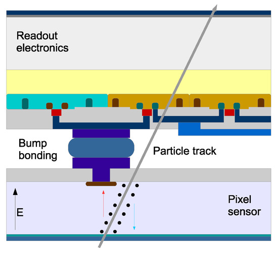
Figure 1. Diagram of a hybrid pixel detector.
A promising alternative to the current hybrid approach is the so-called depleted monolithic active pixel sensors (DMAPS). These kind of detectors integrate the sensing diode and the readout electronics in the same Complementary Metal-Oxide-Semiconductor (CMOS) wafer, as shown in Figure 2. The charge is mainly collected by drift in the depleted volume created by applying a reverse bias voltage to the sensor which generates a strong electric field. The main goal is to create a depleted region in the sensor with a sufficient thickness to collect a reasonably large signal. The thickness of the depleted volume will be proportional to the square root of the sensor resistivity times the reverse bias voltage applied (d∝ρV−−−√). For instance, for a silicon sensor with a p-substrate resistivity of 10 Ω·cm and a bias voltage of 100 V, a depletion depth of about 10 μm would be reached and the collected signal for a MIP (Minimum Ionizing Particle) would be about 700 electrons. With a p-substrate resistivity of 1 kΩ·cm and the same bias voltage, a depletion depth of about 100 μm would be reached and the collected signal for a MIP would be about 7000 electrons. Therefore, the maximum depletion thickness will depend on the CMOS process used to manufacture the DMAP sensor, with a given p-substrate resistivity and a maximum bias voltage limit. Totally depleted sensor operation will be preferred but this will depend on the total thickness of the DMAP sensor which is usually between 70 and 300 μm.
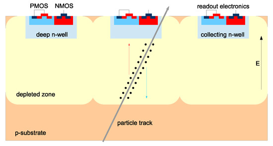
Figure 2. Diagram of a depleted Complementary Metal-Oxide-Semiconductor (CMOS) depleted monolithic active pixel sensors (DMAPS) sensor.
The pixel electronics is placed inside an isolated n-well. Electrons are collected in the n-well to have a faster charge collection. Depending on the sensor capacitance, a charge sensitive amplifier or a voltage amplifier (only for very low input capacitance) will be implemented to convert the collected charge to an equivalent voltage. The noise is proportional to the total capacitance at the input of the amplifier. Therefore, the detector capacitance is a very important parameter to keep the noise low. This sensor technology offers the possibility of noise reduction and higher signal sensitivity compared to the hybrid pixel detectors.
An important advantage of CMOS DMAPS is that their commercial CMOS fabrication process and their integration leads to an easier production, a large cost reduction and a faster fabrication. The size of DMAPS will be constrained by the wafer sizes used in the CMOS process to manufacture the sensors (standard sizes up to 200 and 300 mm can be used currently). Furthermore, this technology can save material budget due to its reduced thickness. Unfortunately, although the depleted CMOS sensor technology offers several clear advantages, there are some aspects which still have to be improved, as the radiation tolerance, the timing resolution and the readout capability to cope with high particle rates.
2. Large Versus Small Fill-Factor Structures
The two main n-on-p CMOS sensor design concepts according to their collection electrode size, known as the fill-factor, are depicted in Figure 3 and Figure 4. In the large fill-factor structure (Figure 3) the sensing diode is made up of the p-substrate and the deep n-well while the electronics are placed inside the charge collection well. High resistivity substrates, up to 3 kΩ·cm [3], are currently available for this structure. In the large fill-factor structure there will be on average shorter drift distances. Moreover, a high bias voltage can be applied to the device, up to 280 V [3], leading to a higher radiation tolerance capability. However, the sensor capacitance is large in this structure, up to hundreds of fF [4] depending on the pixel size, so the noise will be also large. The electronics will also have lower speed and will need more power to counterbalance this fact. Furthermore, this structure is more prone to cross talk from digital electronics into sensor.
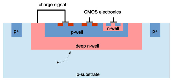
Figure 3. Diagram of a depleted CMOS DMAPS sensor with large fill-factor structure.
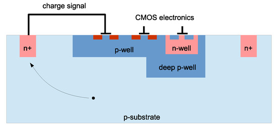
Figure 4. Diagram of a depleted CMOS DMAPS sensor with small fill-factor structure.
On the other hand, the small fill-factor structure (Figure 3) is characterized by the fact that the sensor diode and the readout electronics are separated by the p-substrate. Higher resistivity substrates, up to 8 kΩ·cm [3], can be used with this structure but only low bias voltage, up to 20 V [3], can be applied to the substrate. Moreover, longer drift distances are required on average and consequently, this structure tends to a lower radiation tolerance. Nevertheless, the sensor capacitance is very small, a few fF [4], having a lower noise compared to the large fill-factor structure. Thus, the electronics implemented in the small fill-factor structure can be faster and less power-consuming. There is a fabrication method for sensors with small fill-factor structure to reduce the drift distances by using an additional low dose n-implant to ensure sensor depletion over the entire pixel area at low bias voltages [5].
3. Summary of CMOS Activities in the Framework of the CERN RD50 Collaboration
The CERN RD50 [6] is an international collaboration with more than 300 members aimed at developing and characterizing radiation-hard semiconductor devices for high luminosity colliders. As it has been mentioned, semiconductor sensors will be exposed in the HL-LHC or FCC to hadron fluences not withstood by current LHC sensors. Among other research interests, the collaboration has a research line in new detector structures, such as n-on-p sensors, 3D sensors, low gain avalanche photodiodes and depleted CMOS sensors. The latter are a priority for RD50. In fact, several depletion depth and charge collection measurements have been already carried out with different CMOS devices [7][8]. Moreover, there is a new program within the RD50 collaboration to develop different matrices of pixels and test structures in depleted CMOS processes. This program covers different topics such as TCAD simulations, ASIC design, DAQ development and device characterization. About 36 people from 12 institutes are involved in this program. Two depleted CMOS sensor prototypes had been manufactured within the RD50 collaboration so far, the RD50-MPW1 and the RD50-MPW2, both as MPW (Multi-project Wafer) in the 150 nm LFoundry High-Voltage CMOS (HV-CMOS) process. Currently, there is a third device being designed using the same technology, the RD50-MPW3. After the RD50-MPW3 characterization, the manufacturing of a larger demonstrator, the RD50-ENGRUN1, is foreseen as an enginering run in the 150 nm LFoundry HV-CMOS process.
3.1. RD50-MPW1
The RD50-MPW1 chip [9] has a size of 5 mm by 5 mm and a total thickness of 280 μm. It was submitted in November 2017 and received in April 2014. The RD50-MPW1 was fabricated using substrates of two different resistivities, 500 Ω·cm and 1.9 kΩ·cm. The main goals of this design were to test the technology used and verify the validity of novel designs. Figure 5 shows a diagram of the RD50-MPW1 pixel cross-section, where it can be seen that the device has a large fill-factor structure. The RD50-MPW1 device has test structures for I-V and Edge-Transient Current Technique (E-TCT) measurements and two independent CMOS pixels matrices. One is a photon counting matrix with 28 by 52 pixels with embedded readout electronics, charge amplifier and discriminator, and a 16-bit counter. The other matrix has 40 by 78 pixels, with a size of 50 μm by 50 μm, with embedded readout electronics following a column drain readout architecture similar to the FEI3 readout chip [10].
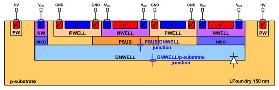
Figure 5. Diagram of the RD50-MPW1 depleted CMOS sensor pixel cross-section.
Concerning the RD50-MPW1 characterization, the leakage current and the breakdown voltage were measured in the pixels of the test structures. E-TCT measurements were also carried out using the test structures. A specific DAQ was developed in order to characterize both active CMOS pixel matrices [11]. The sensors are fully functional but the measured leakage current was found higher than expected [9][12]. Crosstalk was also detected in some digital readout lines from pixels of the matrix with column drain readout architecture [13][14].
3.2. RD50-MPW2
A second device, the RD50-MPW2 [15], was designed to test new design approaches to minimize the leakage current by preventing certain filling layers added by the foundry and adding a series of guard rings [16]. A new pixel readout electronics design was also implemented to improve the speed of the readout electronics [17][18]. This is a smaller device, with a size of about 3 mm by 2 mm and a thickness of 280 μm. It was submitted for fabrication in January 2019 and received in February 2020. Different substrate resistivities have been used, 10 Ω·cm, 0.5–1.1 kΩ·cm, 1.9 kΩ·cm and between 2 and 3 kΩ·cm. The RD50-MPW2 floorplan can be seen in Figure 6. It consists of I-V and E-TCT test structures, an 8 by 8 pixel matrix of 60 μm by 60 μm pixels with analogue embedded readout, a bandgap voltage reference and a Single Event Upset (SEU) tolerant array.
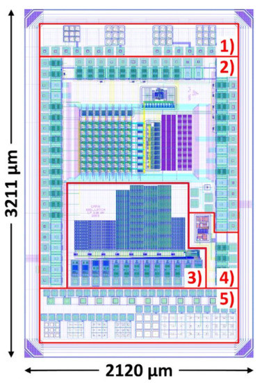
Figure 6. Floorplan of the RD50-MPW2 depleted CMOS sensor with its main blocks highlighted: I–V and E-TCT test structures (1 and 5), 8 by 8 pixel matrix (2), SEU tolerant arrray (3) and bandgap voltage reference (4).
The RD50-MPW2 characterization is still ongoing. The DAQ used to interface the RD50-MPW1 has been updated for this device [19]. Preliminary results show a drastic reduction of about six orders of magnitude of the RD50-MPW2 pixel leakage current, O(100 pA), with respect to the RD50-MPW1 [20], O(100 μA). They also show the correct operation of the pixel matrix [21].
3.3. RD50-MPW3 and RD50-ENGRUN1
A third depleted CMOS sensor prototype, the RD50-MPW3, is currently being designed within the RD50 collaboration. It will be manufactured in the second quarter of 2021 as a MPW in the 150 nm LFoundry HV-CMOS process. This device will have a size of 5 mm by 5 mm and a thickness of 280 μm. It will be manufactured using several substrates of different resistivities. The device will consist of few test structures for I-V and E-TCT measurements and, at least, a matrix of 40 by 78 CMOS pixels with column drain readout architecture. The pixels of this matrix will have the same design and embedded readout as the ones implemented in the RD50-MPW2 device. The matrix column layout is modified with respect to the RD50-MPW1 in order to avoid the crosstalk in some of the digital readout lines. The column drain readout architecture is also improved to optimize the data transmission.
The final objective of the RD50 collaboration depleted CMOS development program is the design of a large area demonstrator in the same technology, the so-called RD50-ENGRUN1 device. A diagram of the main blocks of the RD50-ENGRUN1 device can be seen in Figure 7. This device will consist of several independent depleted CMOS pixel matrices and test structures. The pixel matrices have different purposes and the main goals pursued in this design are the improvement of the current time resolution with dedicated readout circuits, the implementation of new sensor cross-sections, the assessment of pre-stitching options to increase the device size beyond the reticle size limitation and the increase of radiation tolerance by sensor design and backside processing.
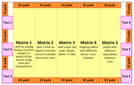
Figure 7. Diagram of the RD50-ENGRUN1 device main blocks.
References
- ATLAS Collaboration. Technical Design Report for the ATLAS Inner Tracker Pixel Detector; CERN-LHCC-2017-021; CERN: Meyrin, Switzerland, 2017.
- CMS Collaboration. The Phase-2 Upgrade of the CMS Tracker (Technical Design Report); CERN-LHCC-2017-009; CERN: Meyrin, Switzerland, 2017.
- Wermes, N. CMOS pixel sensors/detectors overwiew. In Proceedings of the 32nd RD50 Workshop, Hamburg, Germany, 4–6 June 2018.
- Hemperek, T. Overview and perspectives of depleted CMOS sensors for high radiation environments. Proc. Sci. 2017. Available online: https://pos.sissa.it/309/034/pdf (accessed on 27 November 2020).
- Snoeys, W.; Rinella, G.A.; Hillemanns, H.; Kugathasan, T.; Mager, M.; Musa, L.; Riedler, P.; Reidt, F.; Van Hoorne, J.; Fenigstein, A.; et al. A process modification for CMOS monolithic active pixel sensors for enhanced depletion, timing performance and radiation tolerance. Nucl. Inst. Methods Phys. Res. A 2017, 871, 90–96.
- RD50 - Radiation Hard Semiconductor Devices for Very High Luminosity Colliders. Available online: https://rd50.web.cern.ch/ (accessed on 26 November 2020).
- Mandić, I.; Cindro, V.; Gorišek, A.; Hiti, B.; Kramberger, G.; Zavrtanik, M.; Mikuž, M.; Hemperek, T. Charge-collection properties of irradiated depleted CMOS pixel test structures. Nucl. Inst. Methods Phys. Res. 2018, 903, 126–133.
- Cavallaro, E.; Casanova, R.; Förster, F.; Grinstein, S.; Lange, J.; Kramberger, G.; Mandić, I.; Puigdengoles, C.; Terzo, S. Studies of irradiated AMS H35 CMOS detectorsfor the ATLAS tracker upgrade. JINST 2017, 12, C01074.
- Vilella, E.; Alonso, O.; Bergauer, T.; Casanova, R.; Casse, G.; Dieguez, A.; Franks, M.; Grinstein, S.; Irmler, C.; Marco-Hernandez, R.; et al. Overview of design and evaluation of depleted CMOS sensors within RD50. In In Proceedings of the 33rd RD50 Workshop, Geneva, Switzerland, 26–28 November 2018.
- Peri´c, I.; Blanquart, L.; Comes, G.; Denes, P.; Einsweiler, K.; Fischer, P.M.; Elli, E.; Meddeler, G. The FEI3 readout chip for the ATLAS pixel detector. Nucl. Inst. Methods Phys. Res. 2006, 565, 178–187.
- Marco-Hernandez, R. Development of a modular DAQ to characterize the RD50 depleted monolithic active pixel sensors. In Proceedings of the 34th RD50 Workshop, Lancaster, UK, 12–14 June 2019.
- Mandic, I. Irradiation study of CMOS pixel detector structures on RD50-MPW1 chips from LFoundry. In Proceedings of the 33rd RD50 Workshop, CERN, Geneva, Switzerland, 26–28 November 2018.
- Forster, F. LF2/RD50-MPW1 characterization. In Proceedings of the 34th RD50 Workshop, Lancaster, UK, 12–14 June 2019.
- Powell, S.; Vilella, E.; Alonso, O.; Barbero, M.; Casanova, R.; Casse, G.; Dieguez, A.; Franks, M.; Grinstein, S.; Hinojo, J.M.; et al. A status update on the CMOS work package within the CERN-RD50 collaboration. In Proceedings of the 35th RD50 Workshop, Geneva, Switzerland, 18–20 November 2019.
- Vilella, E.; Alonso, O.; Barbero, M.; Casanova, R.; Casse, G.; Dieguez, A.; Franks, M.; Grinstein, S.; Hinojo, J.M.; Lopez, E.; et al. Design work of depleted CMOS sensors within the CERN-RD50 collaboration. In Proceedings of the 34th RD50 Workshop, Lancaster, UK, 12–14 June 2019.
- Franks, M. Design optimisation of depleted CMOS detectors using TCAD simulations within the CERN-RD50 collaboration. In Proceedings of the 14th Trento Workshop on Advanced Radiation Silicon Detectors, Trento, Italy, 25–27 February 2019.
- Zhang, C.; Cassea, G.; Massarib, N.; Vilellaa, E.; Vossebelda, J. Development of RD50-MPW2: A high-speed monolithic HV-CMOS prototype chip within the CERN-RD50 collaboration. In Proceedings of the Topical Workshop on Electronics for Particle Physics, Santiago de Compostela, Spain, 2–6 September 2019.
- Vilella Figueras, E.; RD50 Collaboration. Recent depleted CMOS developments within the CERN-RD50 framework. In Proceedings of the 28th International Workshop on Vertex Detectors, Lopud, Croatia, 13–18 October 2019.
- Irmler, C. Data Acquisition System for Characterization of RD50 HV-CMOS Active Pixel Matrix Prototypes. In Proceedings of the 36th RD50 Workshop, Geneva, Switzerland, 3–5 June 2020.
- Franks, M. Initial I-V and e-TCT measurements of a depleted CMOS sensor within the CERN-RD50 collaboration. In Proceedings of the 36th RD50 Workshop, Geneva, Switzerland, 3–5 June 2020.
- Marco-Hernández, R. First tests and characterization of the RD50-MPW2 active pixel matrix, bandgap voltage reference and SEU tolerant memory. In Proceedings of the 36th RD50 Workshop, Geneva, Switzerland, 3–5 June 2020.

