 +1 credit
| Version | Summary | Created by | Modification | Content Size | Created at | Operation |
|---|---|---|---|---|---|---|
| 1 | Sirius Huang | -- | 2503 | 2022-11-11 01:31:04 |
Video Upload Options
Zen is the codename for a computer processor microarchitecture from AMD, and was first used with their Ryzen series of CPUs in February 2017. The first Zen-based preview system was demonstrated at E3 2016, and first substantially detailed at an event hosted a block away from the Intel Developer Forum 2016. The first Zen-based CPUs codenamed "Summit Ridge" reached the market in early March 2017, Zen-derived Epyc server processors launched in June 2017 and Zen-based APUs arrived in November 2017. Zen is a clean sheet design that differs from the long-standing Bulldozer architecture. Zen-based processors use a 14 nm FinFET process, are reportedly more energy efficient, and can execute significantly more instructions per cycle. SMT has been introduced, allowing each core to run two threads. The cache system has also been redesigned, making the L1 cache write-back. Zen processors use three different sockets: desktop and mobile Ryzen chips use the AM4 socket, bringing DDR4 support; the high-end desktop Zen-based Threadripper chips support quad-channel DDR4 RAM and offer 64 PCIe 3.0 lanes (vs 24 lanes), using the TR4 socket; and Epyc server processors offer 128 PCI 3.0 lanes and octal-channel DDR4 using the SP3 socket. But not all Socket AM4 CPUs are based on Zen microarchitecture (the 7th gen APUs and Athlon X4s are based on Excavator microarchitecture). Zen is based on a SoC design. The memory, PCIe, SATA, and USB controllers are incorporated into the same chip as the processor cores. This has advantages in bandwidth and power, at the expense of chip complexity and die area. This SoC design allows the Zen microarchitecture to scale from laptops and small-form factor mini PCs to high-end desktops and servers.
1. Design
According to AMD, the main focus of Zen is on increasing per-core performance.[1][2][3] New or improved features include:[4]
- The L1 cache has been changed from write-through to write-back, allowing for lower latency and higher bandwidth.
- SMT (simultaneous multithreading) architecture allows for two threads per core, a departure from the CMT (clustered multi-thread) design used in the previous Bulldozer architecture. This is a feature previously offered in some IBM, Intel and Oracle processors.[5]
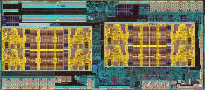
- A fundamental building block for all Zen-based CPUs is the Core Complex (CCX) consisting of four cores and their associated caches. Processors with more than four cores consist of multiple CCXs connected by Infinity Fabric.[6]
- Four ALUs, two AGUs/load–store units, and two floating-point units per core.[7]
- Newly introduced "large" micro-operation cache.[8]
- Each SMT core can dispatch up to six micro-ops per cycle (a combination of 6 integer micro-ops and 4 floating point micro-ops per cycle).[9][10]
- Close to 2× faster L1 and L2 bandwidth, with total L3 cache bandwidth up 5×.
- Clock gating.
- Larger retire, load, and store queues.
- Improved branch prediction using a hashed perceptron system with Indirect Target Array similar to the Bobcat microarchitecture,[11] something that has been compared to a neural network by AMD engineer Mike Clark.[12]
- The branch predictor is decoupled from the fetch stage.
- A dedicated stack engine for modifying the stack pointer, similar to that of Intel Haswell and Broadwell processors.[13]
- Move elimination, a method that reduces physical data movement to reduce power consumption.
- RDSEED support, a set of high-performance hardware random number generator instructions introduced in Intel's Broadwell microarchitecture.[14]
- Support for the SMAP, SMEP, XSAVEC/XSAVES/XRSTORS, XSAVES, CLFLUSHOPT, and CLZERO instructions.[14]
- ADX support.
- SHA support.
- PTE (page table entry) coalescing, which combines 4 kiB page tables into 32 kiB page size.
- "Pure Power" (more accurate power monitoring sensors).[15]
- Smart Prefetch.
- Precision Boost.
- eXtended Frequency Range (XFR), an automated overclocking feature which boosts clock speeds beyond the advertised turbo frequency.[16]
| “ | This is the first time in a very long time that we engineers have been given the total freedom to build a processor from scratch and do the best we can do. It is a multi-year project with a really large team. It's like a marathon effort with some sprints in the middle. The team is working very hard, but they can see the finish line. I guarantee that it will deliver a huge improvement in performance and power consumption over the previous generation. | ” |
| — Suzanne Plummer, Zen team leader, on September 19th, 2015.[17] | ||
The Zen architecture is built on a 14 nanometer FinFET process subcontracted to GlobalFoundries,[18] which in turn licenses its 14 nm process from Samsung Electronics.[19] This gives greater efficiency than the 32 nm and 28 nm processes of previous AMD FX CPUs and AMD APUs, respectively.[20] The "Summit Ridge" Zen family of CPUs use the AM4 socket and feature DDR4 support and a 95 W TDP (thermal design power).[20] While newer roadmaps don't confirm the TDP for desktop products, they suggest a range for low-power mobile products with up to two Zen cores from 5 to 15 W and 15 to 35 W for performance-oriented mobile products with up to four Zen cores.[21]
Each Zen core can decode four instructions per clock cycle and includes a micro-op cache which feeds two schedulers, one each for the integer and floating point segments.[22][23] Each core has two address generation units, four integer units, and four floating point units. Two of the floating point units are adders, and two are multiply-adders. However, using multiply-add-operations may prevent simultaneous add operation in one of the adder units.[24] There are also improvements in the branch predictor. The L1 cache size is 64 KiB for instructions per core and 32 KiB for data per core. The L2 cache size 512 KiB per core, and the L3 is 1–2 MB per core. L3 caches offer 5× the bandwidth of previous AMD designs.
2. History and Development
AMD began planning the Zen microarchitecture shortly after re-hiring Jim Keller in August 2012.[25] AMD formally revealed Zen in 2015.
The team in charge of Zen was led by Keller (who left in September 2015 after a 3-year tenure) and Zen Team Leader Suzanne Plummer.[26][27] The Chief Architect of Zen was AMD Senior Fellow Michael Clark.[28][29][30]
Zen was originally planned for 2017 following the ARM64-based K12 sister core, but on AMD's 2015 Financial Analyst Day it was revealed that K12 was delayed in favor of the Zen design, to allow it to enter the market within the 2016 timeframe,[31] with the release of the first Zen-based processors expected for October 2016.[32]
In November 2015, a source inside AMD reported that Zen microprocessors had been tested and "met all expectations" with "no significant bottlenecks found".[33][34]
In December 2015, it was rumored that Samsung may have been contracted as a fabricator for AMD's 14 nm FinFET processors, including both Zen and AMD's then-upcoming Polaris GPU architecture.[35] This was clarified by AMD's July 2016 announcement that products had been successfully produced on Samsung's 14 nm FinFET process.[36] AMD stated Samsung would be used "if needed", arguing this would reduce risk for AMD by decreasing dependence on any one foundry.
In December 2019, AMD started putting out first generation Ryzen products built using the second generation Zen+ architecture.[37]
3. Advantages over Predecessors
3.1. Manufacturing Process
Processors based on Zen use 14 nm FinFET silicon.[38] These processors are reportedly produced at GlobalFoundries[39] Prior to Zen, AMD's smallest process size was 28 nm, as utilized by their Steamroller and Excavator microarchitectures.[40][41] The immediate competition, Intel's Skylake and Kaby Lake microarchitecture, are also fabricated on 14 nm FinFET;[42] though Intel planned to begin the release of 10 nm parts later in 2017.[43] In comparison to Intel's 14 nm FinFET, AMD claimed in February 2017 the Zen cores would be 10% smaller.[44] Intel has later announced in July 2018 that 10nm mainstream processors should not be expected before the second half of 2019.[45]
For identical designs, these die shrinks would use less current (and power) at the same frequency (or voltage). As CPUs are usually power limited (typically up to ~125 W, or ~45 W for mobile), smaller transistors allow for either lower power at the same frequency, or higher frequency at the same power.[46]
3.2. Performance
One of Zen's major goals in 2016 was to focus on performance per-core, and it was targeting a 40% improvement in instructions per cycle (IPC) over its predecessor.[47] Excavator, in comparison, offered 4–15% improvement over previous architectures.[48][49] AMD announced the final Zen microarchitecture actually achieved 52% improvement in IPC over Excavator.[50] The inclusion of SMT also allows each core to process up to two threads, increasing processing throughput by better use of available resources.
The Zen processors also employ sensors across the chip to dynamically scale frequency and voltage.[51] This allows for the maximum frequency to be dynamically and automatically defined by the processor itself based upon available cooling.
AMD has demonstrated an 8-core/16-thread Zen processor outperforming an equally-clocked Intel Broadwell-E processor in Blender rendering[52][53] and HandBrake benchmarks.[51]
Zen supports AVX2 but it requires two clock cycles to complete each AVX2 instruction compared to Intel's one.[54][55]
3.3. Memory
Zen supports DDR4 memory (up to eight channels)[56] and ECC.[57]
Pre-release reports stated APUs using the Zen architecture would also support High Bandwidth Memory (HBM).[58] However, the first demonstrated APU did not use HBM.[59] Previous APUs from AMD relied on shared memory for both the GPU and the CPU.
3.4. Power Consumption and Heat Output
Processors built at the 14 nm node on FinFET silicon should show reduced power consumption and therefore heat over their 28 nm and 32 nm non-FinFET predecessors (for equivalent designs), or be more computationally powerful at equivalent heat output/power consumption.
Zen also uses clock gating,[23] reducing the frequency of underutilized portions of the core to save power. This comes from AMD's SenseMI technology, using sensors across the chip to dynamically scale frequency and voltage.[51]
3.5. Enhanced Security and Virtualization Support
Zen added support for AMD's Secure Memory Encryption (SME) and AMD's Secure Encrypted Virtualization (SEV). Secure Memory Encryption is real-time memory encryption done per page table entry. Encryption occurs on a hardware AES engine and keys are managed by the onboard "Security" Processor (ARM Cortex-A5) at boot time to encrypt each page, allowing any DDR4 memory (including non-volatile varieties) to be encrypted. AMD SME also makes the contents of the memory more resistant to memory snooping and cold boot attacks.[60][61]
| “ | SME can be used to mark individual pages of memory as encrypted through the page tables. A page of memory that is marked encrypted will be automatically decrypted when read from DRAM and will be automatically encrypted when written to DRAM. The SME feature is identified through a CPUID function and enabled through the SYSCFG MSR. Once enabled, page table entries will determine how the memory is accessed. If a page table entry has the memory encryption mask set, then that memory will be accessed as encrypted memory. The memory encryption mask (as well as other related information) is determined from settings returned through the same CPUID function that identifies the presence of the feature. | ” |
[62]
The Secure Encrypted Virtualization (SEV) feature allows the memory contents of a virtual machine (VM) to be transparently encrypted with a key unique to the guest VM. The memory controller contains a high-performance encryption engine which can be programmed with multiple keys for use by different VMs in the system. The programming and management of these keys is handled by the AMD Secure Processor firmware which exposes an API for these tasks.[63]
3.6. Connectivity
Incorporating much of the southbridge into the SoC, the Zen CPU includes SATA, USB, and PCI Express NVMe links.[64][65] This can be augmented by available Socket AM4 chipsets which add connectivity options including additional SATA and USB connections, and support for AMD's Crossfire and Nvidia's SLI.[66]
AMD, in announcing its Radeon Instinct line, argued that the upcoming Zen-based Naples server CPU would be particularly suited for building deep learning systems.[67][68] The 128[69] PCIe lanes per Naples CPU allows for eight Instinct cards to connect at PCIe x16 to a single CPU. This compares favorably to the Intel Xeon line, with only 40 PCIe lanes.
4. Products
The Zen architecture is used in the current-generation desktop Ryzen CPUs. It is also in Epyc server processors (successor of Opteron processors), and APUs.[58][70][71]
The first desktop processors without graphics processing units (codenamed "Summit Ridge") were initially expected to start selling at the end of 2016, according to an AMD roadmap; with the first mobile and desktop processors of the AMD Accelerated Processing Unit type (codenamed "Raven Ridge") following in late 2017.[72] AMD officially delayed Zen until Q1 of 2017. In August 2016, an early demonstration of the architecture showed an 8-core/16-thread engineering sample CPU at 3.0 GHz.[53]
In December 2016, AMD officially announced the desktop CPU line under the Ryzen brand for release in Q1 2017. It also confirmed Server processors would be released in Q2 2017, and mobile APUs in H2 2017.[73]
On March 2, 2017, AMD officially launched the first Zen architecture-based octacore Ryzen desktop CPUs. The final clock speeds and TDPs for the 3 CPUs released in Q1 of 2017 demonstrated significant performance-per-watt benefits over the previous K15h (Piledriver) architecture.[74][75] The octacore Ryzen desktop CPUs demonstrated performance-per-watt comparable to Intel's Broadwell octacore CPUs.[76][77]
In March 2017, AMD also demonstrated an engineering sample of a server CPU based on the Zen architecture. The CPU (codenamed "Naples") was configured as a dual-socket server platform with each CPU having 32 cores/64 threads.[52][53]
4.1. Desktop Processors
First Generation of Ryzen processors (Ryzen 1000 series)
4.2. Desktop APUs
Ryzen APUs are identified by either the G or GE suffix in their name.
4.3. Mobile APUs
| Model | Release date |
CPU | GPU | Memory support | TDP | Part number | ||||||||
|---|---|---|---|---|---|---|---|---|---|---|---|---|---|---|
| Cores (threads) |
Clock rate (GHz) | Cache[78] | Model | Config[79] | Clock | Processing power (GFLOPS)[80] |
||||||||
| Base | Boost | L1 | L2 | L3 | ||||||||||
| Athlon Pro 200U [81] | 2019 | 2 (4) | 2.3 | 3.2 | 64 KB inst. 32 KB data per core |
512 KB per core |
4 MB | Vega 3 | 192:12:4 3 CU |
1000 MHz | 384 | DDR4-2400 dual-channel |
12–25W | YM200UC4T2OFB |
| Athlon 300U [82] | January 6, 2019 | 2.4 | 3.3 | YM300UC4T2OFG | ||||||||||
| Ryzen 3 2200U [83] | January 8, 2018 | 2.5 | 3.4 | 1100 MHz | 422.4 | YM2200C4T2OFB | ||||||||
| Ryzen 3 3200U [84] | January 6, 2019 | 2.6 | 3.5 | 1200 MHz | 460.8 | YM3200C4T2OFG | ||||||||
| Ryzen 3 2300U [85] | January 8, 2018 | 4 (4) | 2.0 | 3.4 | Vega 6 | 384:24:8 6 CU |
1100 MHz | 844.8 | YM2300C4T4MFB | |||||
| Ryzen 3 Pro 2300U [86] | May 15, 2018 | YM230BC4T4MFB | ||||||||||||
| Ryzen 5 2500U [87] | October 26, 2017 | 4 (8) | 3.6 | Vega 8 | 512:32:16 8 CU |
1126.4 | YM2500C4T4MFB | |||||||
| Ryzen 5 Pro 2500U [88] | May 15, 2018 | YM250BC4T4MFB | ||||||||||||
| Ryzen 5 2600H [89] | September 10, 2018 | 3.2 | DDR4-3200 dual-channel |
35–54W | YM2600C3T4MFB | |||||||||
| Ryzen 7 2700U [90] | October 26, 2017 | 2.2 | 3.8 | Vega 10 | 640:40:16 10 CU |
1300 MHz | 1664 | DDR4-2400 dual-channel |
12–25W | YM2700C4T4MFB | ||||
| Ryzen 7 Pro 2700U [91] | May 15, 2018 | YM270BC4T4MFB | ||||||||||||
| Ryzen 7 2800H [92] | September 10, 2018 | 3.3 | Vega 11 | 704:44:16 11 CU |
1830.4 | DDR4-3200 dual-channel |
35–54W | YM2800C3T4MFB | ||||||
- ↑ AMD in its technical documentation uses KB, which it defines as Kilobyte and as equal to 1024 bytes, and MB, which it defines as Megabyte and as equal to 1024 KB.[93]
- ↑ Unified Shaders : Texture Mapping Units : Render Output Units and Compute Units (CU)
- ↑ Single precision performance is calculated from the base (or boost) core clock speed based on a FMA operation.
4.4. Embedded Processors
In February 2018, AMD announced the V1000 series of embedded Zen+Vega APUs with four SKUs.[94]
4.5. Server Processors
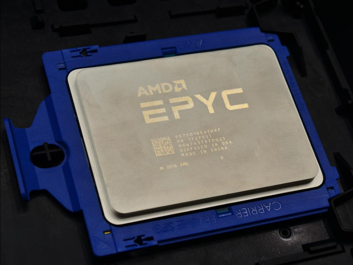
AMD announced in March 2017 that it would release a server platform based on Zen, codenamed Naples, in the second quarter of the year. The platform include 1- and 2-socket systems. The CPUs in multi-processor configurations communicate via AMD's Infinity Fabric.[95] Each chip supports eight channels of memory and 128 PCIe 3.0 lanes, of which 64 lanes are used for CPU-to-CPU communication through Infinity Fabric when installed in a dual-processor configuration.[96] AMD officially revealed Naples under the brand name Epyc in May 2017.[97]
On June 20, 2017, AMD officially released the Epyc 7000 series CPUs at a launch event in Austin, Texas.[98]
4.6. Embedded Server Processors
In February 2018, AMD also announced the EPYC 3000 series of embedded Zen CPUs.[99]
References
- "Weekend tech reading: AMD 'Zen' and their return to high-end CPUs, tracking Windows pirates - TechSpot". techspot.com. http://www.techspot.com/news/60626-tech-reading-amd-zen-comeback.html. Retrieved 2015-05-12.
- "AMD: Zen chips headed to desktops, servers in 2016 - The Tech Report - Page 1". techreport.com. http://techreport.com/review/28228/amd-zen-chips-headed-to-desktops-servers-in-2016. Retrieved 2015-05-12.
- Anton Shilov (11 September 2014). "AMD: ‘Bulldozer’ was not a game-changer, but next-gen ‘Zen’ will be". KitGuru. http://www.kitguru.net/components/cpu/anton-shilov/amd-bulldozer-was-not-a-game-changer-but-next-gen-zen-x86-core-will-be/. Retrieved 1 February 2015.
- Software Optimization Guide for AMD Family 17h Processors / AMD, June 2017 https://support.amd.com/TechDocs/55723_SOG_Fam_17h_Processors_3.00.pdf
- "AMD Zen Confirmed for 2016, Features 40% IPC Improvement Over Excavator". http://techfrag.com/2015/05/08/amd-zen-confirmed-for-2016-features-40-ipc-improvement-over-excavator/.
- Ian Cutress (2017-03-02). "The Core Complex, Caches, and Fabric". http://www.anandtech.com/show/11170/the-amd-zen-and-ryzen-7-review-a-deep-dive-on-1800x-1700x-and-1700/9. Retrieved 2017-06-21.
- Clark, Mike. "A New x86 Core Architecture for the Next Generation of Computing". AMD. p. 7. Archived from the original on 2016-11-26. https://web.archive.org/web/20161126170540/http://www.hotchips.org/wp-content/uploads/hc_archives/hc28/HC28.23-Tuesday-Epub/HC28.23.90-High-Perform-Epub/HC28.23.930-X86-core-MikeClark-AMD-final_v2-28.pdf.
- Cutress, Ian. "AMD Zen Microarchitecture: Dual Schedulers, Micro-Op Cache and Memory Hierarchy Revealed". http://www.anandtech.com/show/10578/amd-zen-microarchitecture-dual-schedulers-micro-op-cache-memory-hierarchy-revealed.
- Mujtaba, Hassan. "AMD Opens The Lid on Zen Architectural Details at Hot Chips – Huge Performance Leap Over Excavator, Massive Throughput on 14nm FinFET Design". http://wccftech.com/amd-zen-architecture-hot-chips/. Retrieved 23 August 2016.
- Walrath, Josh. "AMD Zen Architecture Overview: Focus on Ryzen | PC Perspective" (in en). https://www.pcper.com/reviews/Processors/AMD-Zen-Architecture-Overview-Focus-Ryzen. Retrieved 13 March 2017.
- Jiménez, Daniel. "Strided Sampling Hashed Perceptron Predictor". Texas A&M University. http://www.jilp.org/cbp2014/paper/DanielJimenez.pdf.
- Williams, Chris. "'Neural network' spotted deep inside Samsung's Galaxy S7 silicon brain". https://www.theregister.co.uk/2016/08/22/samsung_m1_core/.
- Fog, Agner. "The microarchitecture of Intel, AMD and VIA CPUs". Technical University of Denmark. http://www.agner.org/optimize/microarchitecture.pdf.
- "AMD Starts Linux Enablement On Next-Gen "Zen" Architecture". Phoronix. 17 March 2015. https://www.phoronix.com/scan.php?page=news_item&px=AMD-Zen-CPU-Znver1. Retrieved 17 March 2015.
- "AMD Takes Computing to a New Horizon with Ryzen™ Processors". https://www.amd.com/en-us/press-releases/Pages/amd-takes-computing-2016dec13.aspx.
- Chen, Sam (24 June 2017). "XFR". https://www.custompcreview.com/wiki/xfr/.
- Kirk Ladendorf - For the American-Statesman. "Amid challenges, chipmaker AMD sees a way forward". http://www.mystatesman.com/news/business/amid-challenges-chipmnaker-amd-sees-a-way-forward/nngdf/.
- Lilly, Paul (23 July 2016), "AMD Shipping Zen In Limited Quantity Q4, Volume Rollout Ramps Q1 2017", hothardware.com, http://hothardware.com/news/amd-shipping-zen-in-limited-volumes-q4, "Zen is being built on an advanced GlobalFoundries-sourced 14nm FinFET process"
- Schor, David (2018-07-22). "VLSI 2018: GlobalFoundries 12nm Leading-Performance, 12LP" (in en-US). https://fuse.wikichip.org/news/1497/vlsi-2018-globalfoundries-12nm-leading-performance-12lp/.
- "14nm AMD Zen CPU Will Have DDR4 and Simultaneous Multithreading". Softpedia. 28 January 2015. http://news.softpedia.com/news/14nm-AMD-Zen-CPU-Will-Have-DDR4-and-Simultaneous-Multithreading-471401.shtml. Retrieved 31 January 2015.
- "AMD's next gen CPU Zen". Shattered.Media. May 2015. Archived from the original on 2015-11-17. https://web.archive.org/web/20151117024542/http://www.shattered.media/amds-next-gen-cpu-zen/.
- "AMD's Zen core (family 17h) to have ten pipelines per core". http://dresdenboy.blogspot.fi/2015/10/amds-zen-core-family-17h-to-have-ten.html.
- Cutress, Ian (18 August 2016). "AMD Zen Microarchitecture". Anandtech. http://www.anandtech.com/show/10578/amd-zen-microarchitecture-dual-schedulers-micro-op-cache-memory-hierarchy-revealed. Retrieved 18 August 2016.
- AMD, "Software Optimization Guider for AMD Family 17h Processors"
- Jim Keller On AMD's Next-Gen High Performance x86 Zen Core & K12 ARM Core. YouTube. 7 May 2014. https://www.youtube.com/watch?v=SOTFE7sJY-Q
- "Jim Keller Leaves AMD". Anand tech. http://anandtech.com/show/9643/jim-keller-leaves-amd. Retrieved 2015-10-14.
- Ladendorf, Kirk. "Amid challenges, chipmaker AMD sees a way forward" (in en). https://www.statesman.com/business/20160904/amid-challenges-chipmaker-amd-sees-a-way-forward.
- Merritt, Rick (24 August 2016). "AMD Reveals Zen of X86". EE Times. http://www.eetimes.com/document.asp?doc_id=1330348. Retrieved 3 March 2017.
- TAKAHASHI, Dean (24 August 2016). "How AMD designed what could be its most competitive processors in a decade". VentureBeat. https://venturebeat.com/2016/08/24/how-amd-designed-what-could-be-its-most-competitive-processors-in-a-decade/. Retrieved 3 March 2017.
- Wong, Adrian (18 April 2017). "Joe Macri : The Disruptive Nature of AMD Ryzen". TechArp. http://www.techarp.com/articles/joe-macri-disruptive-nature-amd-ryzen/. Retrieved 20 April 2017.
- Ryan Smith (6 May 2015). "AMD’s 2016-2017 x86 Roadmap: Zen Is In, Skybridge Is Out". AnandTech. http://www.anandtech.com/show/9231/amds-20162017-x86-roadmap-zen-is-in.
- "AMD set to release first ‘Zen’-based microprocessors in late 2016 – document". 12 June 2015. http://www.kitguru.net/components/cpu/anton-shilov/amd-set-to-release-first-zen-based-microprocessors-in-late-2016-document. Retrieved 30 August 2015.
- "GlobalFoundries announces 14nm validation with AMD Zen silicon". ExtremeTech. http://www.extremetech.com/computing/217664-globalfoundries-announces-14nm-validation-with-amd-silicon.
- "OC3D :: Article :: AMD Tests Zen CPUs, "Met All Expectation" with no "Significant Bottlenecks" found :: AMD Tests Zen CPUs, Met All Expectation with no Significant Bottlenecks found". http://www.overclock3d.net/articles/cpu_mainboard/amd_tests_zen_cpus_met_all_expectation_with_no_significant_bottlenecks_found/1.
- "Samsung to fab AMD Zen & Arctic islands on its 14 nm Finfet node", Tech power up .
- Moorhead, Patrick (25 July 2016). "AMD Officially Diversifies 14nm Manufacturing With Samsung". Forbes. https://www.forbes.com/sites/patrickmoorhead/2016/07/25/amd-diversifies-14nm-manufacturing-with-samsung/#4e63559550fb. Retrieved 26 July 2016.
- "First-Gen AMD Ryzen CPUs are Appearing with 12nm Zen+ Architecture". 2019-12-22. https://wccftech.com/first-gen-amd-ryzen-cpus-are-appearing-with-12nm-zen-architecture/.
- "AMD’s next-gen CPU leak: 14nm, simultaneous multithreading, and DDR4 support". ExtremeTech. http://www.extremetech.com/extreme/198386-amds-next-gen-cpu-leak-14nm-simultaneous-multithreading-and-ddr4-support.
- Rulison, Larry (22 August 2016). "Reports: Chip made by GlobalFoundries beats Intel". Times Union. http://www.timesunion.com/local/article/Reports-Chip-made-by-GlobalFoundries-beats-Intel-9176925.php. Retrieved 22 August 2016.
- "AMD: We have taped out our first FinFET products". KitGuru. http://www.kitguru.net/components/graphic-cards/anton-shilov/amd-we-have-taped-out-our-first-finfet-products/.
- "CES: AMD finally unveils 28nm APU Kaveri to battle Intel Haswell". The Inquirer. http://www.theinquirer.net/inquirer/news/2321439/ces-amd-finally-unveils-28nm-apu-kaveri-to-battle-intel-haswell.
- "Intel Kaby Lake to compete against AMD Zen at end of 2016". 2016-03-02. http://www.digitimes.com/news/a20160302PD204.html. Retrieved 2016-03-07. "Intel's Kaby Lake-series processors, which are scheduled to launch in the third quarter, but will not begin volume production until the end of 2016, while AMD is set to release its Zen architecture-based processors at the end of the fourth quarter."
- Edward Jones (21 Oct 2016). "AMD Zen: A serious challenge to Intel?". Channel Pro. http://www.channelpro.co.uk/advice/9797/amd-zen-a-serious-challenge-to-intel-7.
- Manion, Wayne (8 February 2017). "AMD touts Zen die size advantage at ISSCC". Tech Report. https://techreport.com/news/31402/amd-touts-zen-die-size-advantage-at-isscc. Retrieved 10 February 2017.
- https://arstechnica.com/gadgets/2018/07/intel-says-not-to-expect-mainstream-10nm-chips-until-2h19/
- "Intel’s ‘Tick-Tock’ Seemingly Dead, Becomes ‘Process-Architecture-Optimization’". http://www.anandtech.com/show/10183/intels-tick-tock-seemingly-dead-becomes-process-architecture-optimization. Retrieved 23 March 2016.
- Smith, Ryan (31 May 2016). "AMD Briefly Shows Off Zen "Summit Ridge" Silicon". http://www.anandtech.com/show/10391/amd-briefly-shows-off-zen-summit-ridge-silicon. Retrieved 7 June 2016.
- "AMD Announces Zen, 40% IPC Improvement Over Excavator - Coming In 2016". 7 May 2015. http://wccftech.com/amd-zen-architecture-release-schedule-revealed-rolled-server-market/.
- Ian Cutress (June 2, 2015). "IPC Increases: Double L1 Data Cache, Better Branch Prediction - AMD Launches Carrizo: The Laptop Leap of Efficiency and Architecture Updates". Anandtech. http://www.anandtech.com/show/9319/amd-launches-carrizo-the-laptop-leap-of-efficiency-and-architecture-updates/4.
- Cutress, Ian (22 February 2017). "AMD Launches Zen". Anandtech.com. http://www.anandtech.com/show/11143/amd-launch-ryzen-52-more-ipc-eight-cores-for-under-330-preorder-today-on-sale-march-2nd. Retrieved 22 February 2017.
- Kampman, Jeff (13 December 2016). "AMD crests Summit Ridge with Ryzen CPUs". TechReport. https://techreport.com/review/31105/amd-crests-summit-ridge-with-ryzen-cpus. Retrieved 13 December 2016.
- Anthony, Sebastian (18 August 2016). "AMD says Zen CPU will outperform Intel Broadwell-E, delays release to 2017". Ars Technica. https://arstechnica.com/gadgets/2016/08/amd-zen-performance-details-release-date/. Retrieved 18 August 2016.
- Kampman, Jeff (18 August 2016). "AMD gives us our first real moment of Zen". Tech Report. https://techreport.com/review/30540/amd-gives-us-our-first-real-moment-of-zen. Retrieved 18 August 2016.
- Cutress, Ian. "AMD Zen Microarchiture Part 2: Extracting Instruction-Level Parallelism". http://www.anandtech.com/show/10591/amd-zen-microarchiture-part-2-extracting-instructionlevel-parallelism/7.
- Leadbetter, Richard (22 February 2017). "In Theory: How AMD's Ryzen will disrupt the gaming CPU market". http://www.eurogamer.net/articles/digitalfoundry-2017-how-amds-ryzen-will-disrupt-the-cpu-market.
- "AMD's Zen processors to feature up to 32 cores, 8-channel DDR4". TechSpot. http://www.techspot.com/news/63796-amd-zen-cpu-up-32-cores.html.
- MAC (30 March 2017). "ECC Memory & AMD's Ryzen - A Deep Dive". Hardware Canucks. http://www.hardwarecanucks.com/forum/hardware-canucks-reviews/75030-ecc-memory-amds-ryzen-deep-dive.html. Retrieved 14 July 2017.
- "Zen-based APU with HBM to be AMD Carrizo successor". http://hexus.net/tech/news/cpu/89246-zen-based-apu-hbm-amd-carrizo-successor/.
- Shrout, Ryan (30 May 2017). "Computex 2017: AMD Demos Ryzen Mobile SoC with Vega Graphics". PC Perspective. https://www.pcper.com/news/Processors/Computex-2017-AMD-Demos-Ryzen-Mobile-SoC-Vega-Graphics. Retrieved 2 June 2017.
- "[RFC PATCH v1 00/18 x86: Secure Memory Encryption (AMD)"]. http://lkml.iu.edu/hypermail/linux/kernel/1604.3/02551.html.
- "AMD MEMORY ENCRYPTION WHITEPAPER". http://developer.amd.com/wordpress/media/2013/12/AMD_Memory_Encryption_Whitepaper_v7-Public.pdf.
- "LKML - Tom Lendacky (AMD) explains AMD Secure Memory Encryption". http://lkml.iu.edu/hypermail/linux/kernel/1604.3/02533.html.
- "AMD - Other Developer Guides: Secure Encrypted Virtualization Key Management PDF – 05/19/2016". http://support.amd.com/TechDocs/55766_SEV-KM%20API_Spec.pdf.
- L, Alex; Walrath, Josh (12 January 2017). "Podcast #432 - Kaby Lake, Vega, CES Review". PC Perspective. https://www.pcper.com/news/Editorial/Podcast-432-Kaby-Lake-Vega-CES-Review. Retrieved 13 January 2017.
- Mah Ung, Gordon (28 September 2016). "How AMD's powerful Zen chip flouts the SoC stereotype". PC World. http://www.pcworld.com/article/3124306/hardware/dont-call-amds-upcoming-zen-chip-a-cpu.html. Retrieved 13 January 2017.
- Justin, Michael; Sexton, Allen (3 March 2017). "AMD's AM4 Ryzen Chipsets". Tom's Hardware. http://www.tomshardware.com/news/amd-am4-ryzen-chipsets,33806.html. Retrieved 3 March 2017.
- Smith, Ryan (12 December 2016). "AMD Announces Radeon Instinct: GPU Accelerators for Deep Learning, Coming in 2017". Anandtech. http://www.anandtech.com/show/10905/amd-announces-radeon-instinct-deep-learning-2017. Retrieved 12 December 2016.
- Shrout, Ryan (12 December 2016). "Radeon Instinct Machine Learning GPUs include Vega, Preview Performance". PC Per. https://www.pcper.com/reviews/Graphics-Cards/Radeon-Instinct-Machine-Learning-GPUs-include-Vega-Preview-Performance. Retrieved 12 December 2016.
- Mujtaba, Hassan (2017-03-07). "AMD Naples High-Performance Server Chips With 32 Cores, 64 Threads Detailed" (in en-US). Wccftech. https://wccftech.com/amd-naples-server-chip-32-core-64-thread-preview/.
- "AMD Zen FX CPUs, APUs Release Details Surface, Top-Notch Performance In The Cards". Tech Times. http://www.techtimes.com/articles/111041/20151127/amd-zen-fx-cpus-apus-release-details-surface-top-notch-performance-in-the-cards.htm.
- "32-core AMD Opteron to feature quad-die MCM design". KitGuru. http://www.kitguru.net/components/cpu/anton-shilov/32-core-amd-opteron-to-feature-quad-die-mcm-design/.
- Mark Mantel (7 February 2017). "CPU-Roadmap 2017 - 2018: Künftige AMD- und Intel-CPUs/-APUs in der Übersicht" (in German). http://www.pcgameshardware.de/CPU-Hardware-154106/Specials/Roadmap-CPUs-Prozessoren-Liste-AMD-Intel-1130335/.
- Larabel, Michael (13 December 2016). "AMD Reveals More Zen CPU Details, Officially Known As Ryzen, No Linux Details Yet". Phoronix. https://www.phoronix.com/scan.php?page=news_item&px=AMD-Ryzen-New-Horizon. Retrieved 13 December 2016.
- "Power Consumption And Efficiency - AMD FX-8350 Review: Does Piledriver Fix Bulldozer's Flaws?" (in en). Tom's Hardware. 2012-10-22. http://www.tomshardware.com/reviews/fx-8350-vishera-review,3328-16.html.
- "AMD Ryzen 7 1800X: Power Consumption And Temperatures" (in en). Tom's Hardware. 2017-03-02. http://www.tomshardware.com/reviews/amd-ryzen-7-1800x-cpu,4951-11.html.
- "AMD Ryzen 7 1800X and AM4 Platform Review" (in en). bit-tech. https://www.bit-tech.net/hardware/2017/03/02/amd-ryzen-1800x-and-am4-platform-review/8.
- "The AMD Ryzen 7 1800X Review: Now and Zen | Power Consumption and Conclusions" (in en). https://www.pcper.com/reviews/Processors/AMD-Ryzen-7-1800X-Review-Now-and-Zen/Power-Consumption-and-Conclusions.
- AMD in its technical documentation uses KB, which it defines as Kilobyte and as equal to 1024 bytes, and MB, which it defines as Megabyte and as equal to 1024 KB.[88]
- Unified Shaders : Texture Mapping Units : Render Output Units and Compute Units (CU)
- Single precision performance is calculated from the base (or boost) core clock speed based on a FMA operation.
- "AMD Athlon™ PRO 200U Mobile Processor with Radeon™ Vega 3 Graphics". https://www.amd.com/en/product/8201.
- "AMD Athlon™ 300U Mobile Processor with Radeon™ Vega 3 Graphics". https://www.amd.com/en/products/apu/amd-athlon-300u.
- "AMD Ryzen™ 3 2200U". https://www.amd.com/en/products/apu/amd-ryzen-3-2200u.
- "AMD Ryzen™ 3 3200U Mobile Processor with Radeon™ Vega 3 Graphics". https://www.amd.com/en/products/apu/amd-ryzen-3-3200u.
- "AMD Ryzen™ 3 2300U". https://www.amd.com/en/products/apu/amd-ryzen-3-2300u.
- "AMD Ryzen™ 3 PRO 2300U". https://www.amd.com/en/products/apu/amd-ryzen-3-pro-2300u.
- "AMD Ryzen™ 5 2500U". https://www.amd.com/en/products/apu/amd-ryzen-5-2500u.
- "AMD Ryzen™ 5 PRO 2500U". https://www.amd.com/en/products/apu/amd-ryzen-5-pro-2500u.
- "AMD Ryzen™ 5 2600H Mobile Processor with Radeon™ Vega 8 Graphics". https://www.amd.com/en/products/apu/amd-ryzen-5-2600h.
- "AMD Ryzen™ 7 2700U". https://www.amd.com/en/products/apu/amd-ryzen-7-2700u.
- "AMD Ryzen™ 7 PRO 2700U". https://www.amd.com/en/products/apu/amd-ryzen-7-pro-2700u.
- "AMD Ryzen™ 7 2800H Mobile Processor with Radeon™ RX Vega 11 Graphics". https://www.amd.com/en/products/apu/amd-ryzen-7-2800h.
- "Processor Programming Reference (PPR) for AMD Family 17h Model 01h, Revision B1 Processors" (PDF). AMD Technical Documentation. AMD Developer Central: Advanced Micro Devices, Inc.. 2017-04-15. p. 25. http://developer.amd.com/wordpress/media/2017/11/54945_PPR_Family_17h_Models_00h-0Fh.pdf. Retrieved 2019-11-01.
- Alcorn, Paul (21 February 2018). "AMD Launches Ryzen Embedded V1000, EPYC Embedded 3000 Processors". Tomshardware.com. Retrieved 5 April 2018. http://www.tomshardware.com/news/amd-epyc-ryzen-embedded-v1000-3000,36556.html
- Kampman, Jeff (7 March 2017). "AMD's Naples platform prepares to take Zen into the datacenter". Tech Report. https://techreport.com/news/31549/amd-naples-platform-prepares-to-take-zen-into-the-datacenter. Retrieved 7 March 2017.
- Cutress, Ian (7 March 2017). "AMD Prepares 32-Core Naples CPUs for 1P and 2P Servers: Coming in Q2". Anandtech. http://www.anandtech.com/show/11183/amd-prepares-32-core-naples-cpus-for-1p-and-2p-servers-coming-in-q2. Retrieved 7 March 2017.
- Kampman, Jeff (16 May 2017). "AMD's Naples datacenter CPUs will make an Epyc splash". Tech Report. https://techreport.com/news/31916/amd-naples-datacenter-cpus-will-make-an-epyc-splash. Retrieved 16 May 2017.
- "AMD launches broad Epyc server processor line with up to 32 cores per chip". 2017-06-20. https://venturebeat.com/2017/06/20/amd-launches-broad-epyc-server-line-with-up-to-32-cores-per-chip/.
- Alcorn, Paul (21 February 2018). "AMD Launches Ryzen Embedded V1000, EPYC Embedded 3000 Processors". tom's HARDWARE. http://www.tomshardware.com/news/amd-epyc-ryzen-embedded-v1000-3000,36556.html. Retrieved 5 April 2018.

